Scaling sami franssilaaalto fi No autio clips this
- Slides: 43

Scaling sami. franssila@aalto. fi No autio clips this time, standard Zoom-lecture.

Outline CMOS scaling • Wafer size (and thickness) scaling • Wafer specs scaling • Wafer fab scaling • Lithography and etch scaling • Aspect ratio scaling • CMOS oxide and junction scaling Solar scaling Magnetic memory scaling

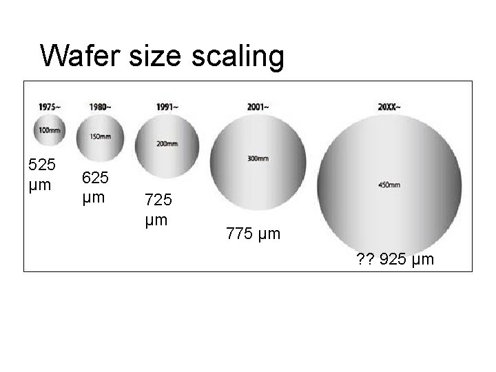
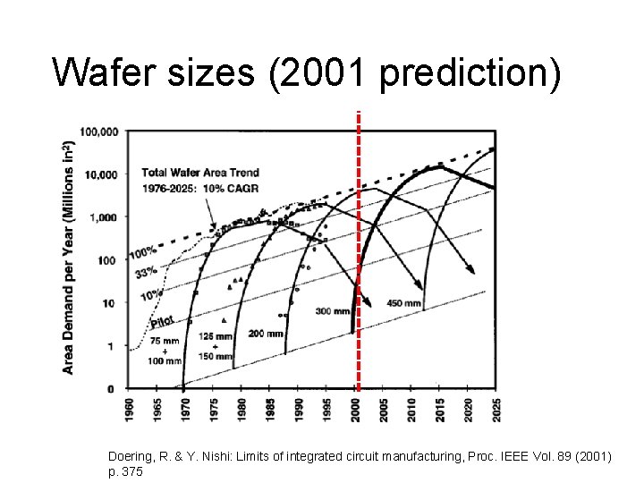
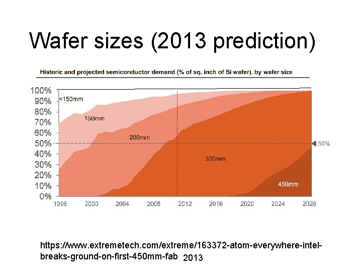
Wafer size scaling 525 µm 625 µm 775 µm ? ? 925 µm

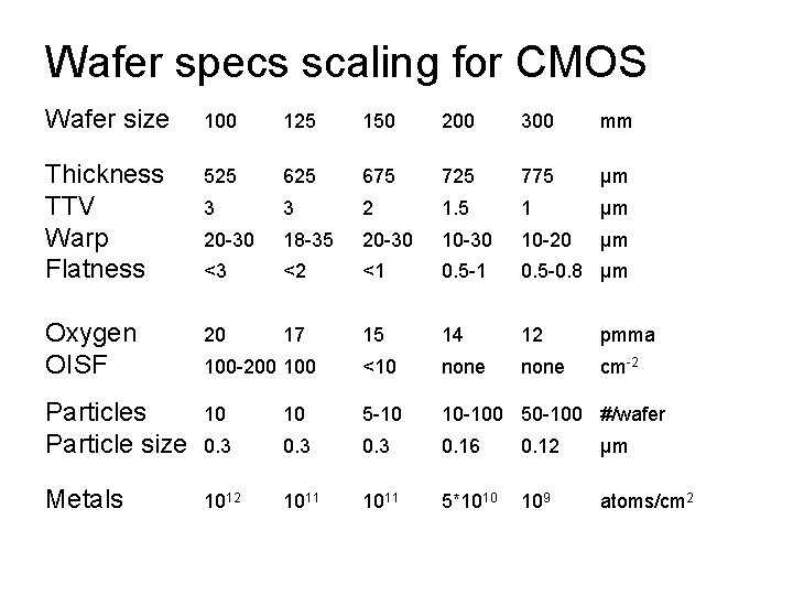
Wafer specs scaling for CMOS Wafer size 100 125 150 200 300 mm Thickness TTV Warp Flatness 525 675 725 775 µm 3 3 2 1. 5 1 µm 20 -30 18 -35 20 -30 10 -20 µm <3 <2 <1 0. 5 -0. 8 µm Oxygen OISF 20 17 15 14 12 pmma 100 -200 100 <10 none cm-2 Particles Particle size 10 10 5 -10 10 -100 50 -100 #/wafer 0. 3 0. 16 0. 12 µm Metals 1012 1011 5*1010 109 atoms/cm 2

Wafer sizes (2001 prediction) Doering, R. & Y. Nishi: Limits of integrated circuit manufacturing, Proc. IEEE Vol. 89 (2001) p. 375

Wafer sizes (2013 prediction) https: //www. extremetech. com/extreme/163372 -atom-everywhere-intelbreaks-ground-on-first-450 mm-fab 2013

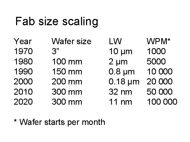
Fab size scaling Year 1970 1980 1990 2000 2010 2020 Wafer size 3” 100 mm 150 mm 200 mm 300 mm * Wafer starts per month LW 10 µm 2 µm 0. 8 µm 0. 18 µm 32 nm 11 nm WPM* 1000 5000 10 000 20 000 50 000 100 000

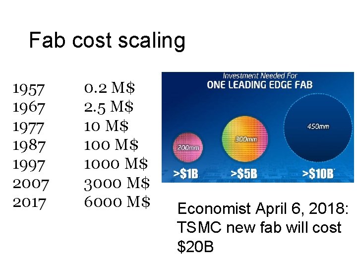
Fab cost scaling 1957 1967 1977 1987 1997 2007 2017 0. 2 M$ 2. 5 M$ 1000 M$ 3000 M$ 6000 M$ Economist April 6, 2018: TSMC new fab will cost $20 B

Making 450 mm etcher “Maximum throughput of an etch tool is governed by two basic factors: 1) wafer load/unload time 2) etch time. With good engineering wafer throughput is independent of wafer size, so that chip throughput improves as the wafer size increases. ” Chris Mack: http: //www. lithoguru. com/scientist/essays/why 450. html

Making 450 mm etcher (2) “But “good engineering” is not free, and it takes work to keep the etch uniformity the same for a larger wafer. The larger etch tools also cost more money to make. But if the tool cost does not increase as fast as the wafer area, the result is a lower cost per chip. This is the goal, and the reason why we pursue larger wafer sizes. “ Chris Mack: http: //www. lithoguru. com/scientist/essays/why 450. html

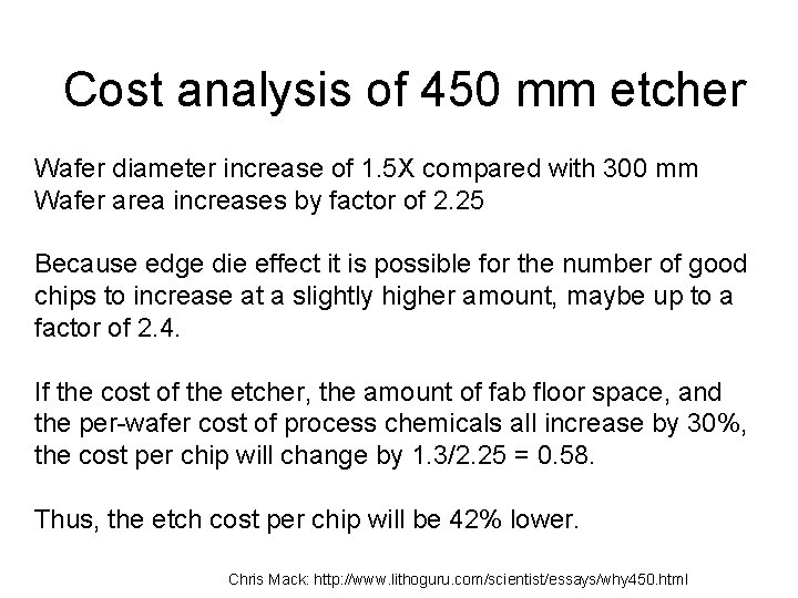
Cost analysis of 450 mm etcher Wafer diameter increase of 1. 5 X compared with 300 mm Wafer area increases by factor of 2. 25 Because edge die effect it is possible for the number of good chips to increase at a slightly higher amount, maybe up to a factor of 2. 4. If the cost of the etcher, the amount of fab floor space, and the per-wafer cost of process chemicals all increase by 30%, the cost per chip will change by 1. 3/2. 25 = 0. 58. Thus, the etch cost per chip will be 42% lower. Chris Mack: http: //www. lithoguru. com/scientist/essays/why 450. html

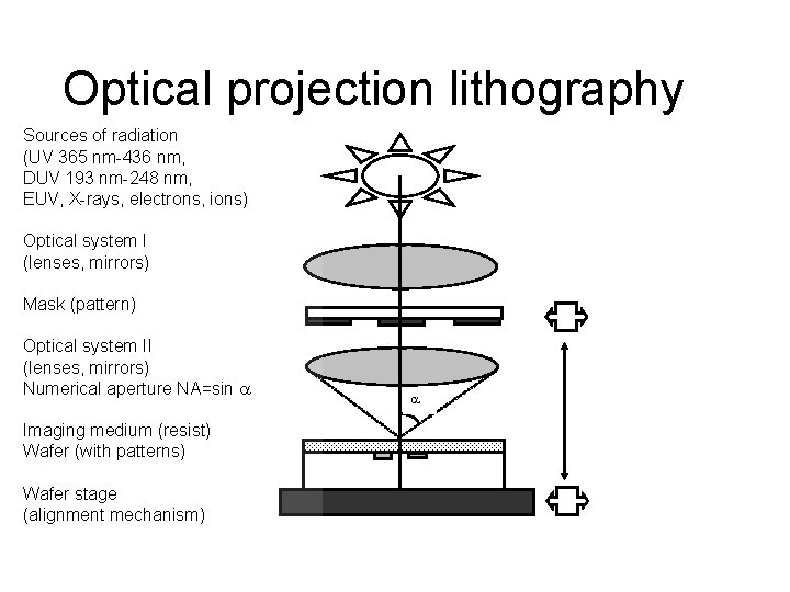
Optical projection lithography Sources of radiation (UV 365 nm-436 nm, DUV 193 nm-248 nm, EUV, X-rays, electrons, ions) Optical system I (lenses, mirrors) Mask (pattern) Optical system II (lenses, mirrors) Numerical aperture NA=sin Imaging medium (resist) Wafer (with patterns) Wafer stage (alignment mechanism)

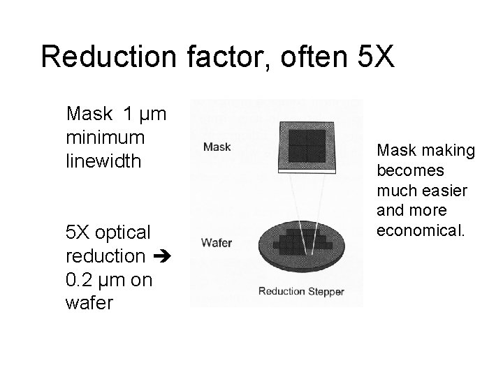
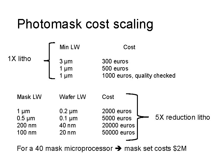
Reduction factor, often 5 X Mask 1 µm minimum linewidth 5 X optical reduction 0. 2 µm on wafer Mask making becomes much easier and more economical.

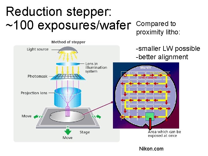
Reduction stepper: ~100 exposures/wafer Compared to proximity litho: -smaller LW possible -better alignment Nikon. com

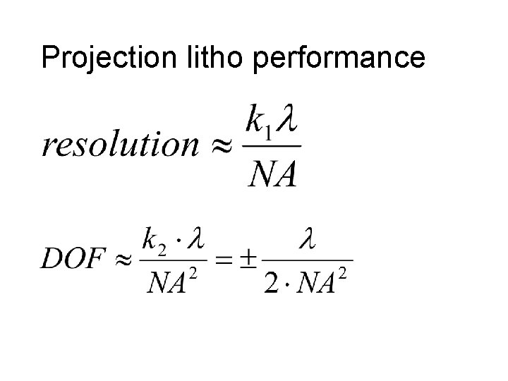
Projection litho performance

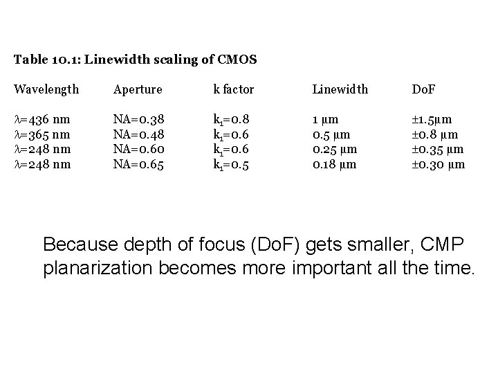
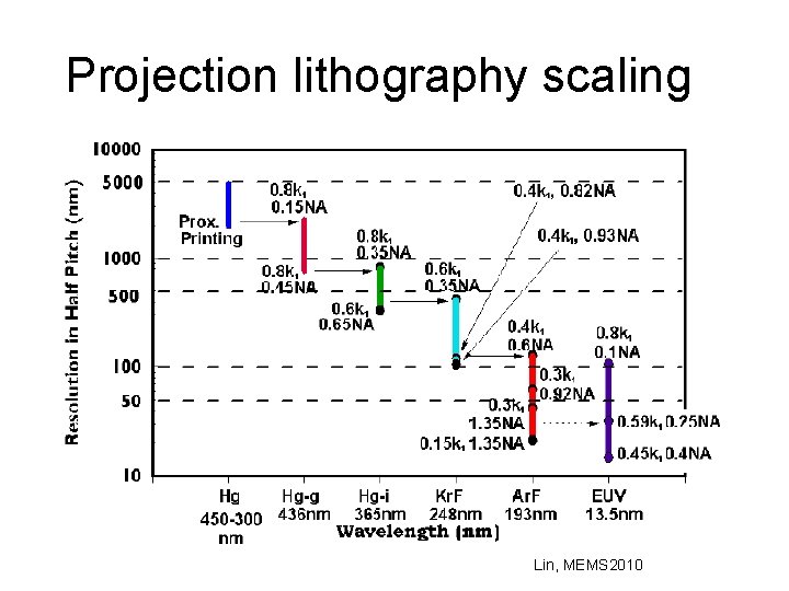
Table 10. 1: Linewidth scaling of CMOS Wavelength Aperture k factor Linewidth Do. F =436 nm =365 nm =248 nm NA=0. 38 NA=0. 48 NA=0. 60 NA=0. 65 k 1=0. 8 k 1=0. 6 k 1=0. 5 1 µm 0. 5 µm 0. 25 µm 0. 18 µm 1. 5µm 0. 8 µm 0. 35 µm 0. 30 µm Because depth of focus (Do. F) gets smaller, CMP planarization becomes more important all the time.

Projection lithography scaling Lin, MEMS 2010

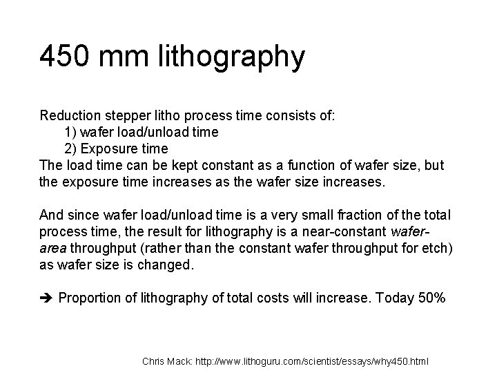
450 mm lithography Reduction stepper litho process time consists of: 1) wafer load/unload time 2) Exposure time The load time can be kept constant as a function of wafer size, but the exposure time increases as the wafer size increases. And since wafer load/unload time is a very small fraction of the total process time, the result for lithography is a near-constant waferarea throughput (rather than the constant wafer throughput for etch) as wafer size is changed. Proportion of lithography of total costs will increase. Today 50% Chris Mack: http: //www. lithoguru. com/scientist/essays/why 450. html

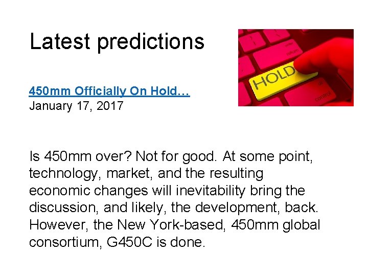
Latest predictions 450 mm Officially On Hold… January 17, 2017 Is 450 mm over? Not for good. At some point, technology, market, and the resulting economic changes will inevitability bring the discussion, and likely, the development, back. However, the New York-based, 450 mm global consortium, G 450 C is done.

Photomask cost scaling Min LW 1 X litho Cost 3 µm 1 µm 300 euros 500 euros 1000 euros, quality checked Mask LW Wafer LW Cost 1 µm 0. 5 µm 200 nm 100 nm 0. 2 µm 0. 1 µm 40 nm 2000 euros 5000 euros 20000 euros 5 X reduction litho For a 40 mask microprocessor mask set costs $2 M

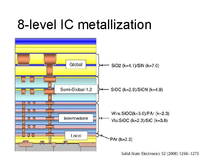
8 -level IC metallization

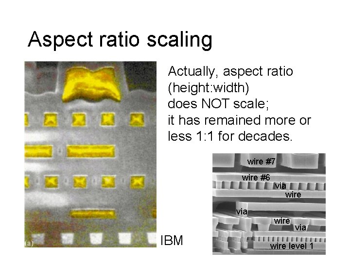
Aspect ratio scaling Actually, aspect ratio (height: width) does NOT scale; it has remained more or less 1: 1 for decades. wire #7 wire #6 via IBM via wire level 1

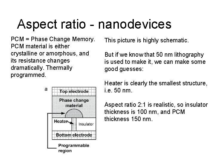
Aspect ratio - nanodevices PCM = Phase Change Memory. PCM material is either crystalline or amorphous, and its resistance changes dramatically. Thermally programmed. This picture is highly schematic. But if we know that 50 nm lithography is used to make it, we can make some good guesses: Heater is clearly the smallest structure, i. e. 50 nm. Aspect ratio 2: 1 is realistic, so insulator thickness is 100 nm, and PCM thickness 150 nm.

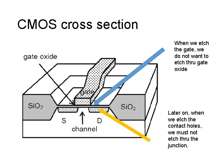
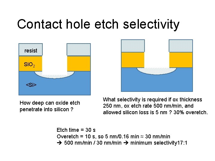
Etch selectivity scaling Case 1: poly: oxide selectivity in gate etching Case 2: contact hole etch selectivity (oxide: silicon)

CMOS cross section When we etch the gate, we do not want to etch thru gate oxide Later on, when we etch the contact holes, we must not etch thru the junction.

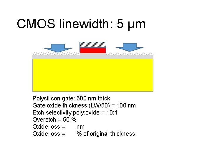
CMOS linewidth: 5 µm Polysilicon gate: 500 nm thick Gate oxide thickness (LW/50) = 100 nm Etch selectivity poly: oxide = 10: 1 Overetch = 50 % Oxide loss = nm Oxide loss = % of original thickness

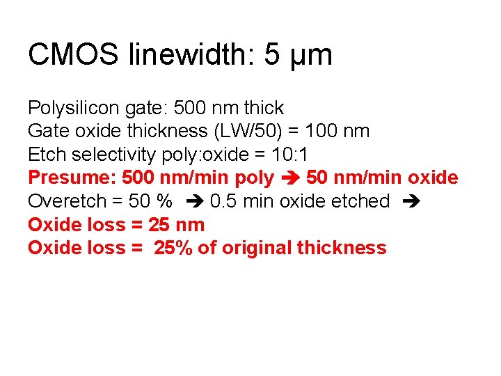
CMOS linewidth: 5 µm Polysilicon gate: 500 nm thick Gate oxide thickness (LW/50) = 100 nm Etch selectivity poly: oxide = 10: 1 Presume: 500 nm/min poly 50 nm/min oxide Overetch = 50 % 0. 5 min oxide etched Oxide loss = 25 nm Oxide loss = 25% of original thickness

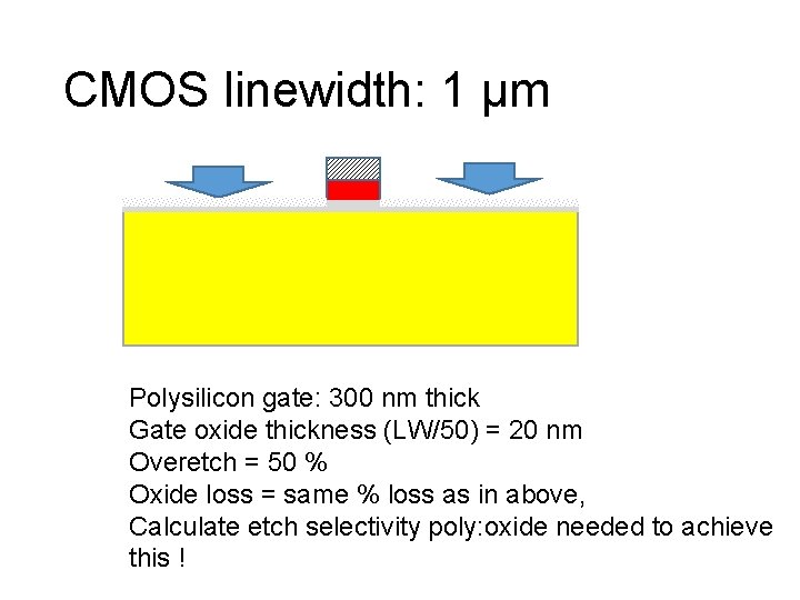
CMOS linewidth: 1 µm Polysilicon gate: 300 nm thick Gate oxide thickness (LW/50) = 20 nm Overetch = 50 % Oxide loss = same % loss as in above, Calculate etch selectivity poly: oxide needed to achieve this !

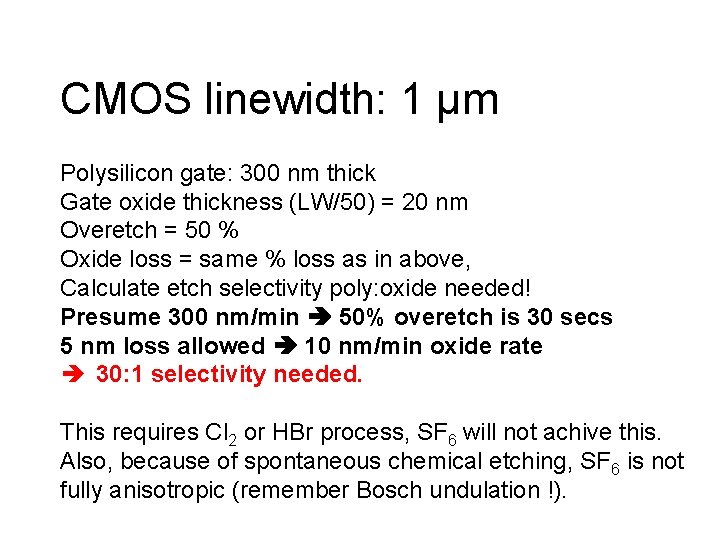
CMOS linewidth: 1 µm Polysilicon gate: 300 nm thick Gate oxide thickness (LW/50) = 20 nm Overetch = 50 % Oxide loss = same % loss as in above, Calculate etch selectivity poly: oxide needed! Presume 300 nm/min 50% overetch is 30 secs 5 nm loss allowed 10 nm/min oxide rate 30: 1 selectivity needed. This requires Cl 2 or HBr process, SF 6 will not achive this. Also, because of spontaneous chemical etching, SF 6 is not fully anisotropic (remember Bosch undulation !).

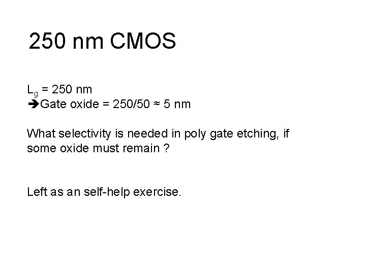
250 nm CMOS Lg = 250 nm Gate oxide = 250/50 ≈ 5 nm What selectivity is needed in poly gate etching, if some oxide must remain ? Left as an self-help exercise.

Contact hole etch selectivity resist Si. O 2 <Si> How deep can oxide etch penetrate into silicon ? What selectivity is required if ox thickness 250 nm, ox etch rate 500 nm/min, and allowed silicon loss is 5 nm ? 30% overetch. Etch time = 30 s Overetch = 10 s, so 5 nm/0. 16 min ≈ 30 nm/min 500 nm/min / 30 nm/min minimum selectivity 17: 1

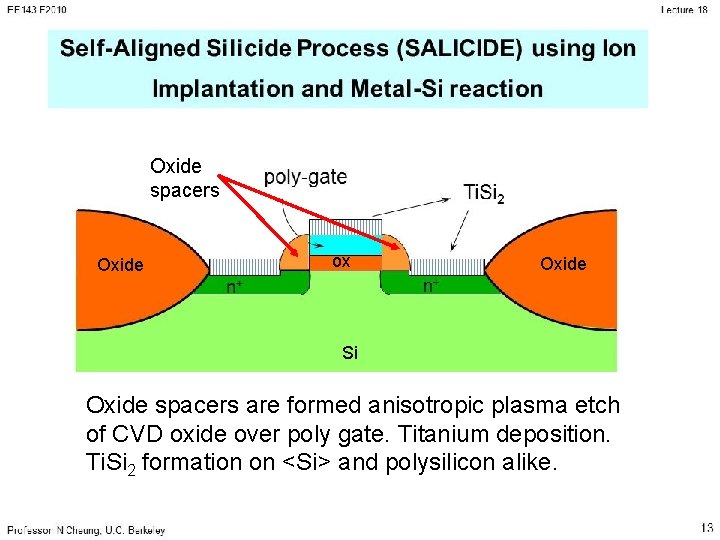
Oxide spacers Oxide ox Oxide Si Oxide spacers are formed anisotropic plasma etch of CVD oxide over poly gate. Titanium deposition. Ti. Si 2 formation on <Si> and polysilicon alike.

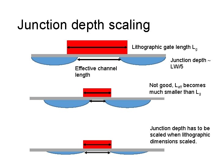
Junction depth scaling Lithographic gate length Lg Effective channel length Junction depth ~ LW/5 Not good, Leff becomes much smaller than Lg Junction depth has to be scaled when lithographic dimensions scaled.

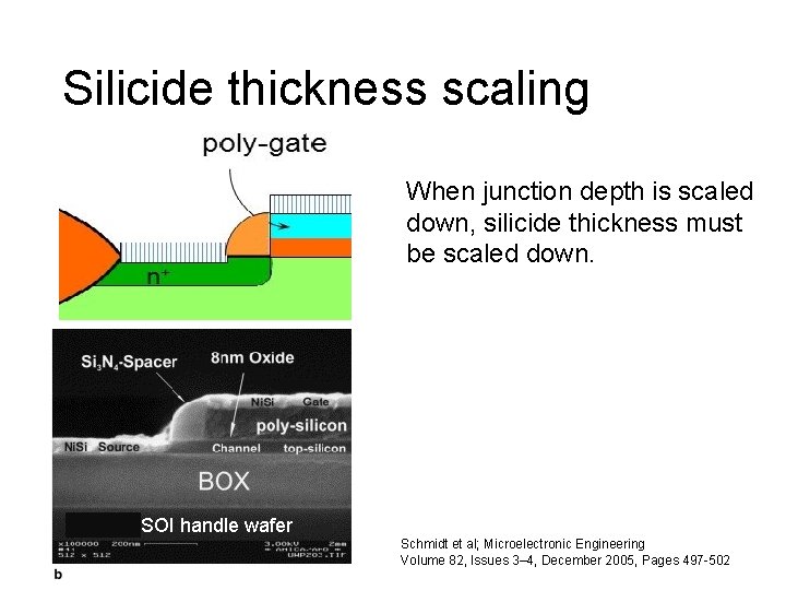
Silicide thickness scaling When junction depth is scaled down, silicide thickness must be scaled down. SOI handle wafer Schmidt et al; Microelectronic Engineering Volume 82, Issues 3– 4, December 2005, Pages 497 -502

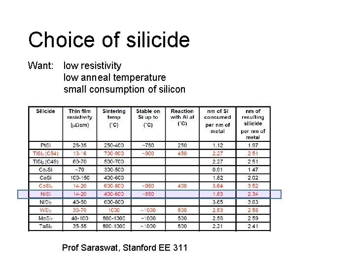
Choice of silicide Want: low resistivity low anneal temperature small consumption of silicon Prof Saraswat, Stanford EE 311

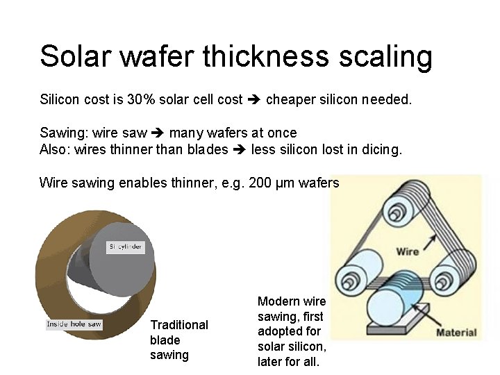
Solar wafer thickness scaling Silicon cost is 30% solar cell cost cheaper silicon needed. Sawing: wire saw many wafers at once Also: wires thinner than blades less silicon lost in dicing. Wire sawing enables thinner, e. g. 200 µm wafers Traditional blade sawing Modern wire sawing, first adopted for solar silicon, later for all.

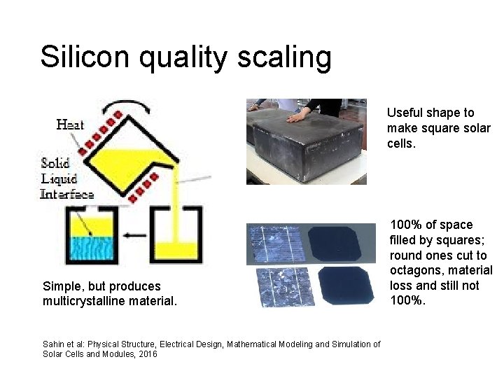
Silicon quality scaling Useful shape to make square solar cells. Simple, but produces multicrystalline material. Sahin et al: Physical Structure, Electrical Design, Mathematical Modeling and Simulation of Solar Cells and Modules, 2016 100% of space filled by squares; round ones cut to octagons, material loss and still not 100%.

Silicon quality scaling …”there is a marginal change in cell efficiency when the dislocation density increases from 102 to 103 cm-2. There is a rapid decrease in efficiency once the dislocation density goes above 104 cm-2. ” Vinay Budhraja. New Jersey Institute of Technology, Ph. D thesis “Unfortunately, nobody knows exactly how pure and that is why manufacturers play it safe. In other words: they generally use too pure and therefore too expensive silicon. ” Dr. Gianluca Coletti, www. ecn. nl

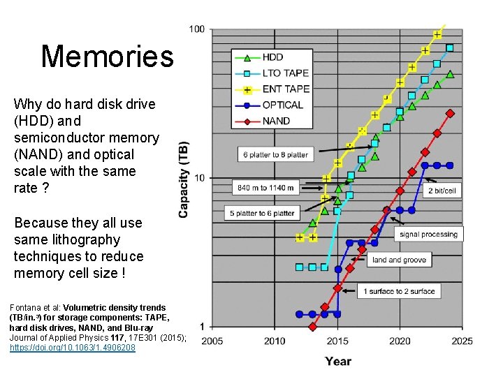
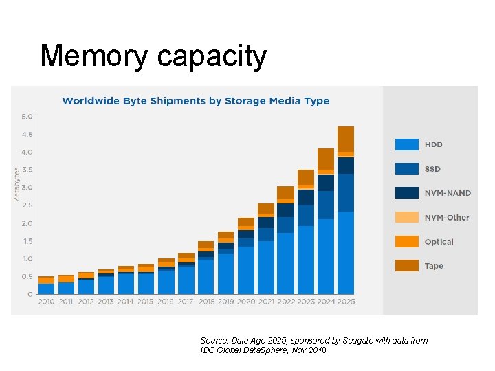
Memories Why do hard disk drive (HDD) and semiconductor memory (NAND) and optical scale with the same rate ? Because they all use same lithography techniques to reduce memory cell size ! Fontana et al: Volumetric density trends (TB/in. 3) for storage components: TAPE, hard disk drives, NAND, and Blu-ray Journal of Applied Physics 117, 17 E 301 (2015); https: //doi. org/10. 1063/1. 4906208

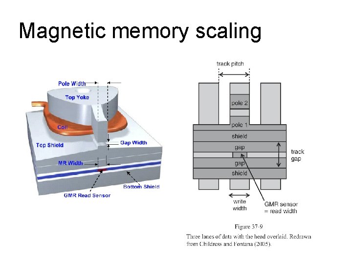
Magnetic memory scaling

Memory capacity Source: Data Age 2025, sponsored by Seagate with data from IDC Global Data. Sphere, Nov 2018

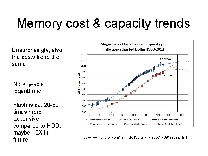
Memory cost & capacity trends Unsurprisingly, also the costs trend the same. Note: y-axis logarithmic. Flash is ca. 20 -50 times more expensive compared to HDD, maybe 10 X in future. https: //www. nedprod. com/Niall_stuff/vdiary/archives/1406483538. html

Take home messages Chip size should be as small as possible. Small linewidths increase costs, but enable smaller chips. Big wafer size reduces costs. If you have money for advanced lithography, you will use big wafers. Big wafer size means thicker wafers for mechanical strength. Thicker wafers not good for thru-wafer MEMS. Thin wafers good for solar, but mechanically weak. High aspect ratios are rare, MEMS and DRAM mostly. Usually aspect ratios are between 1: 2 to 2: 1. With small linewidths, thin films must be thin to keep aspect ratio low.