Thin films sami franssilaaalto fi Thin films different
- Slides: 46

Thin films sami. franssila@aalto. fi

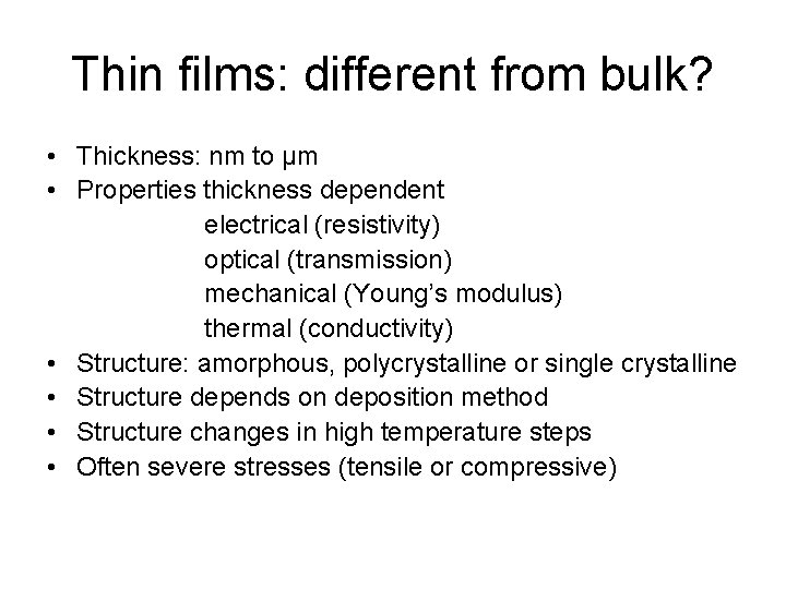
Thin films: different from bulk? • Thickness: nm to µm • Properties thickness dependent electrical (resistivity) optical (transmission) mechanical (Young’s modulus) thermal (conductivity) • Structure: amorphous, polycrystalline or single crystalline • Structure depends on deposition method • Structure changes in high temperature steps • Often severe stresses (tensile or compressive)

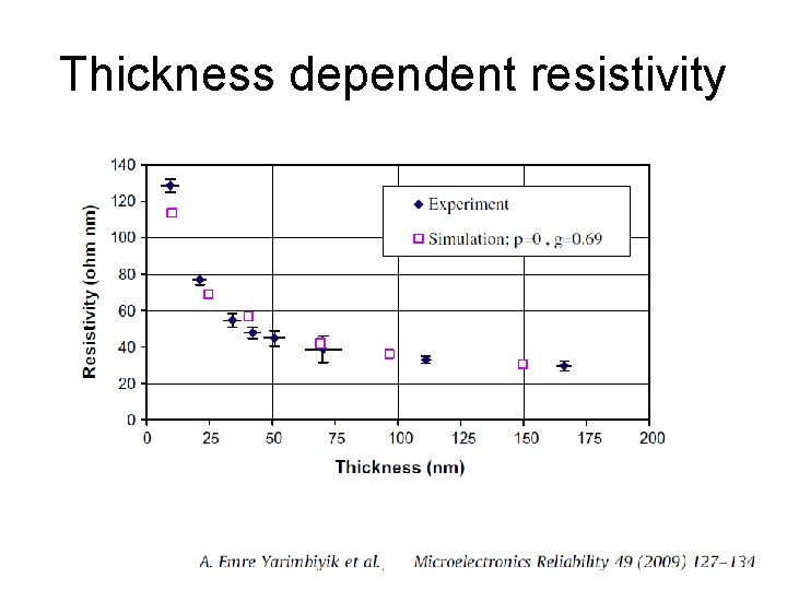
Thickness dependent resistivity

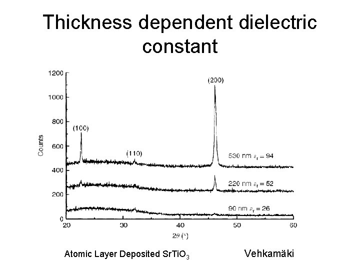
Thickness dependent dielectric constant Atomic Layer Deposited Sr. Ti. O 3 Vehkamäki

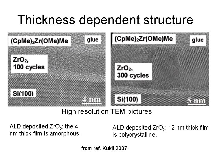
Thickness dependent structure High resolution TEM pictures ALD deposited Zr. O 2: the 4 nm thick film Is amorphous. ALD deposited Zr. O 2: 12 nm thick film is polycrystalline. from ref. Kukli 2007.

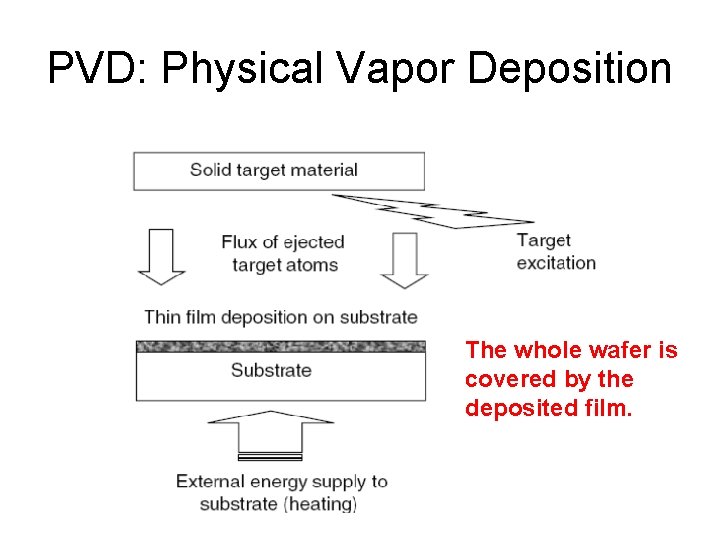
PVD: Physical Vapor Deposition The whole wafer is covered by the deposited film.

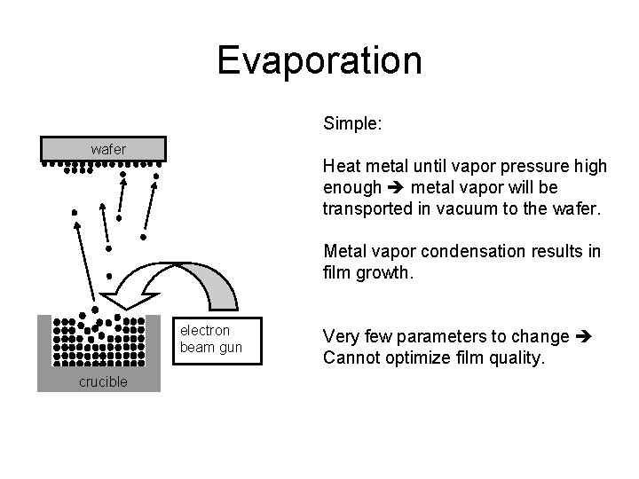
Evaporation Simple: wafer Heat metal until vapor pressure high enough metal vapor will be transported in vacuum to the wafer. Metal vapor condensation results in film growth. electron beam gun crucible Very few parameters to change Cannot optimize film quality.

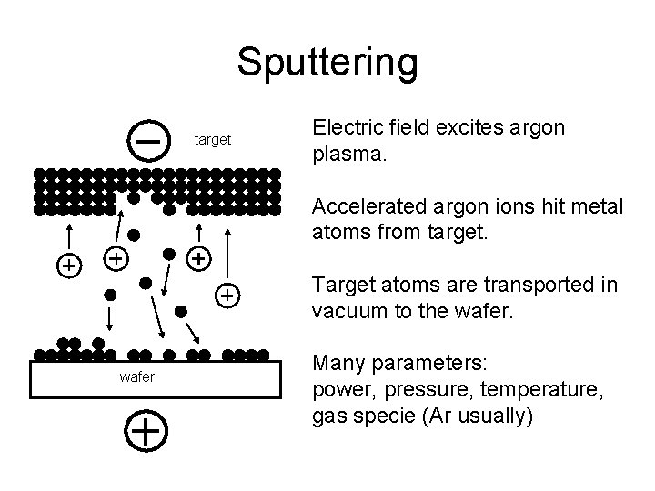
Sputtering target Electric field excites argon plasma. Accelerated argon ions hit metal atoms from target. Target atoms are transported in vacuum to the wafer Many parameters: power, pressure, temperature, gas specie (Ar usually)

Metallic films usually by PVD • • conductors (Al, Au, Cu) resistors (Ta, W, Pt) capacitor electrodes (poly-Si, Al, Mo) mechanical materials (Al-movable mirrors) magnetic materials (Ni coils) protective coatings (Cr, Ni etch masks) optical materials (mirrors, reflectors, IR filters) catalysts (Pt, Pd in chemical sensors)

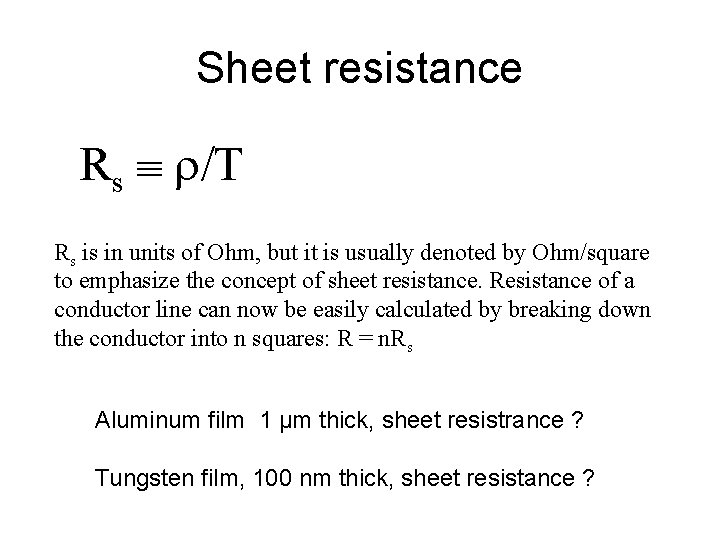
Sheet resistance Rs /T Rs is in units of Ohm, but it is usually denoted by Ohm/square to emphasize the concept of sheet resistance. Resistance of a conductor line can now be easily calculated by breaking down the conductor into n squares: R = n. Rs Aluminum film 1 µm thick, sheet resistrance ? Tungsten film, 100 nm thick, sheet resistance ?

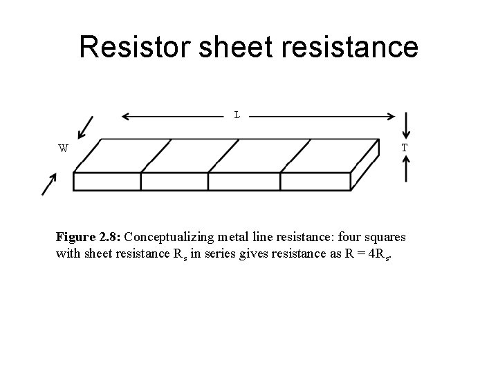
Resistor sheet resistance Figure 2. 8: Conceptualizing metal line resistance: four squares with sheet resistance Rs in series gives resistance as R = 4 Rs.

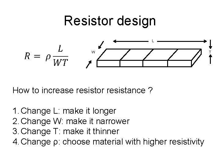
Resistor design L W How to increase resistor resistance ? 1. Change L: make it longer 2. Change W: make it narrower 3. Change T: make it thinner 4. Change ρ: choose material with higher resistivity T

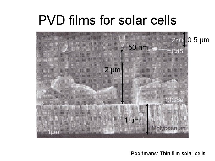
PVD films for solar cells 50 nm 0. 5 µm 2 µm 1 µm Poortmans: Thin film solar cells

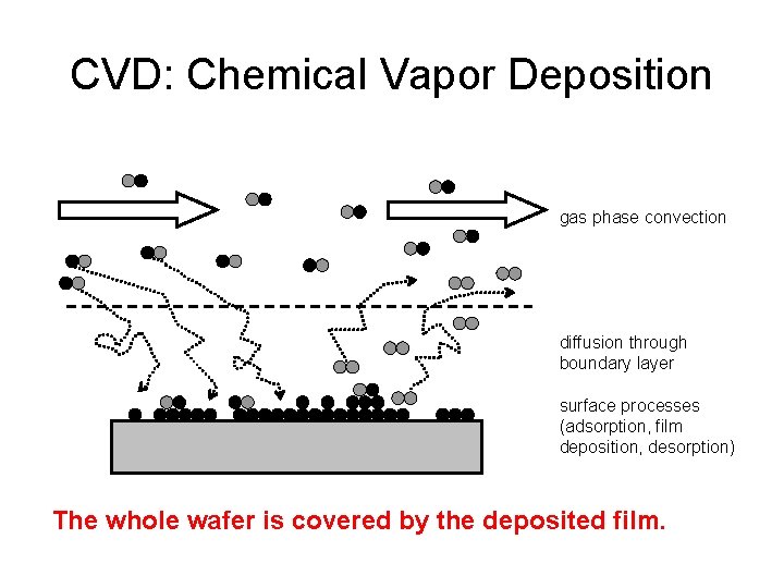
CVD: Chemical Vapor Deposition gas phase convection diffusion through boundary layer surface processes (adsorption, film deposition, desorption) The whole wafer is covered by the deposited film.

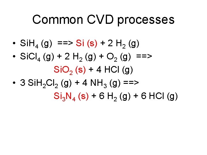
Common CVD processes • Si. H 4 (g) ==> Si (s) + 2 H 2 (g) • Si. Cl 4 (g) + 2 H 2 (g) + O 2 (g) ==> Si. O 2 (s) + 4 HCl (g) • 3 Si. H 2 Cl 2 (g) + 4 NH 3 (g) ==> Si 3 N 4 (s) + 6 H 2 (g) + 6 HCl (g)

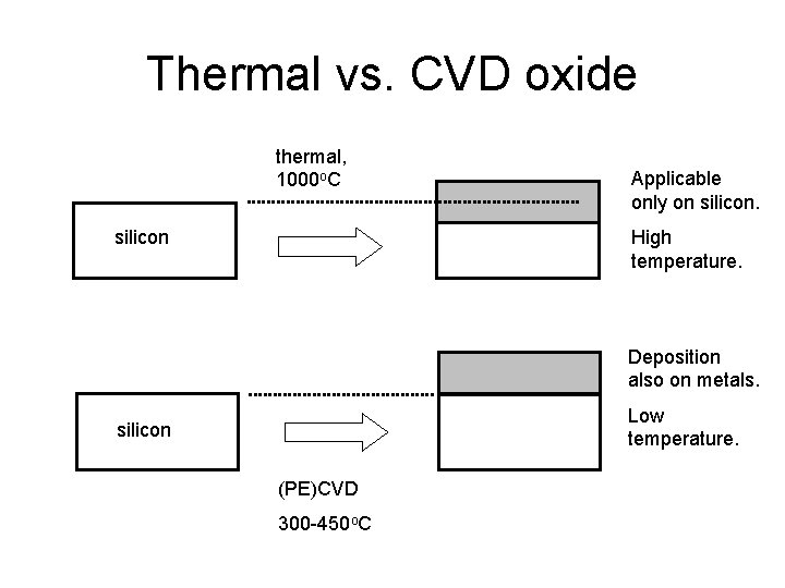
Thermal vs. CVD oxide thermal, 1000 o. C silicon Applicable only on silicon. High temperature. Deposition also on metals. Low temperature. silicon (PE)CVD 300 -450 o. C

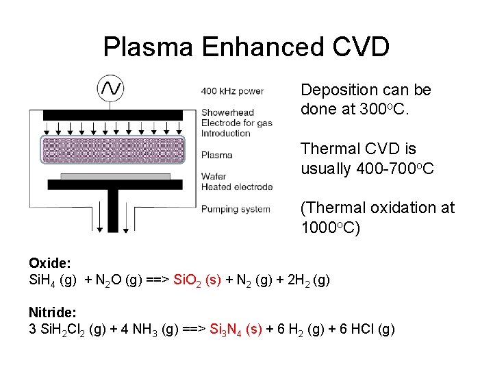
Plasma Enhanced CVD Deposition can be done at 300 o. C. Thermal CVD is usually 400 -700 o. C (Thermal oxidation at 1000 o. C) Oxide: Si. H 4 (g) + N 2 O (g) ==> Si. O 2 (s) + N 2 (g) + 2 H 2 (g) Nitride: 3 Si. H 2 Cl 2 (g) + 4 NH 3 (g) ==> Si 3 N 4 (s) + 6 H 2 (g) + 6 HCl (g)

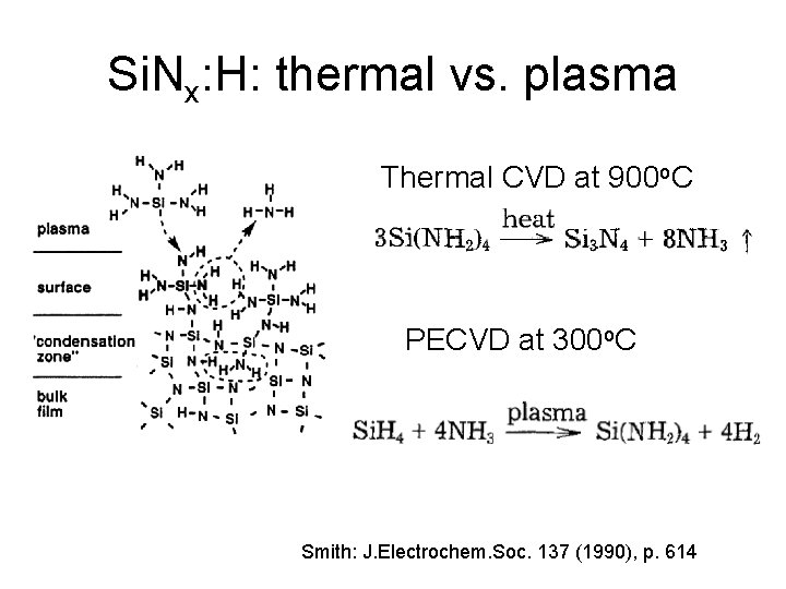
Si. Nx: H: thermal vs. plasma Thermal CVD at 900 o. C PECVD at 300 o. C Smith: J. Electrochem. Soc. 137 (1990), p. 614

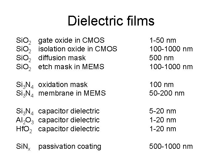
Dielectric films Si. O 2 gate oxide in CMOS isolation oxide in CMOS diffusion mask etch mask in MEMS 1 -50 nm 100 -1000 nm 500 nm 100 -1000 nm Si 3 N 4 oxidation mask Si 3 N 4 membrane in MEMS 100 nm 50 -200 nm Si 3 N 4 capacitor dielectric Al 2 O 3 capacitor dielectric Hf. O 2 capacitor dielectric 5 -20 nm 1 -20 nm Si. Nx 500 -1000 nm passivation coating

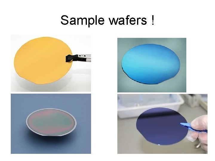
Sample wafers !

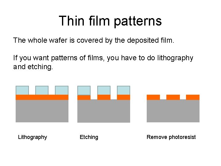
Thin film patterns The whole wafer is covered by the deposited film. If you want patterns of films, you have to do lithography and etching. Lithography Etching Remove photoresist

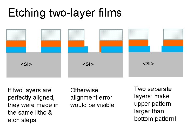
Etching two-layer films <Si> If two layers are perfectly aligned, they were made in the same litho & etch steps. <Si> Otherwise alignment error would be visible. <Si> Two separate layers: make upper pattern larger than bottom pattern!

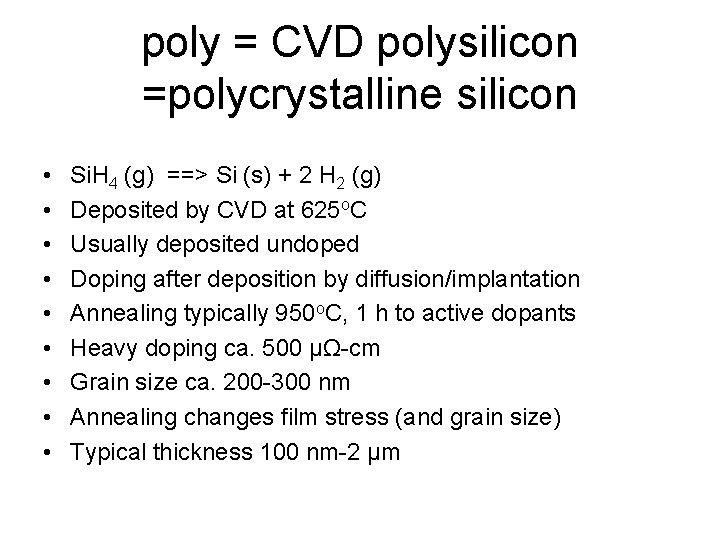
poly = CVD polysilicon =polycrystalline silicon • • • Si. H 4 (g) ==> Si (s) + 2 H 2 (g) Deposited by CVD at 625 o. C Usually deposited undoped Doping after deposition by diffusion/implantation Annealing typically 950 o. C, 1 h to active dopants Heavy doping ca. 500 µΩ-cm Grain size ca. 200 -300 nm Annealing changes film stress (and grain size) Typical thickness 100 nm-2 µm

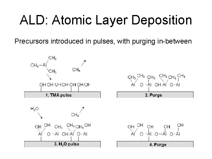
ALD: Atomic Layer Deposition Precursors introduced in pulses, with purging in-between

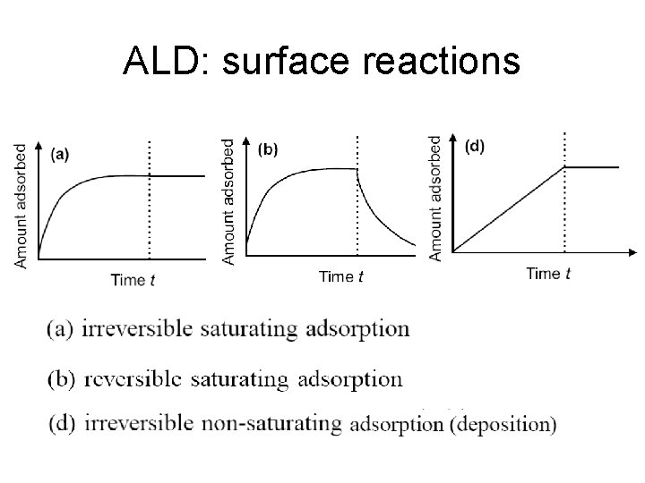
ALD: surface reactions

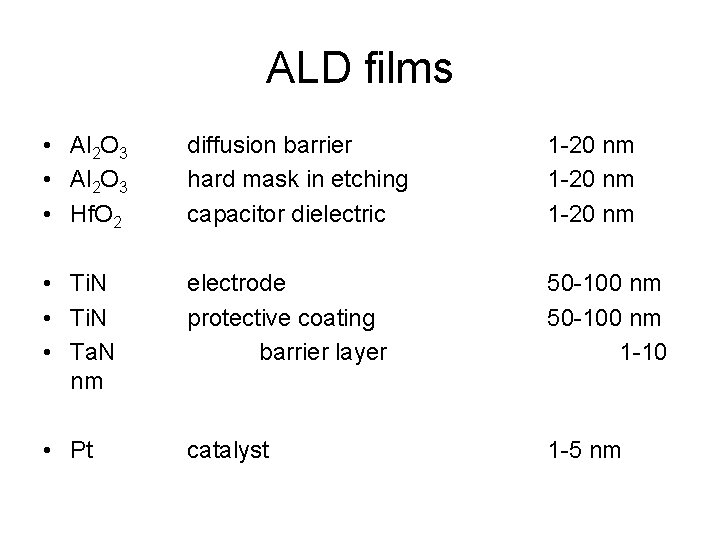
ALD films • Al 2 O 3 • Hf. O 2 diffusion barrier hard mask in etching capacitor dielectric 1 -20 nm • Ti. N • Ta. N nm electrode protective coating barrier layer 50 -100 nm 1 -10 • Pt catalyst 1 -5 nm

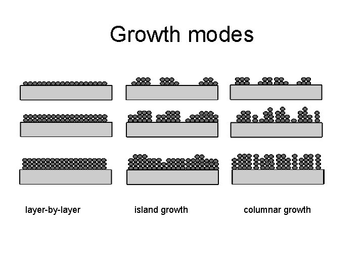
Growth modes layer-by-layer island growth columnar growth

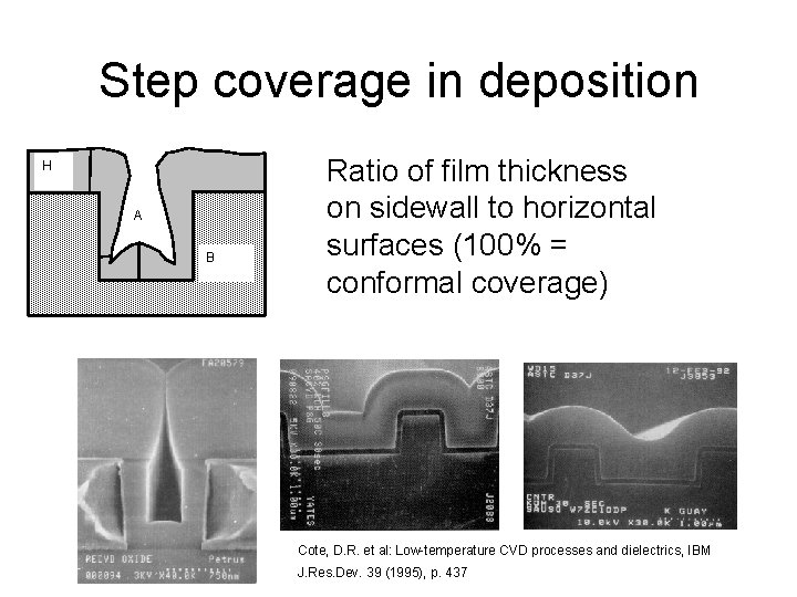
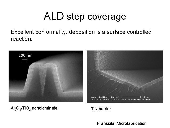
Step coverage in deposition H A B Ratio of film thickness on sidewall to horizontal surfaces (100% = conformal coverage) Cote, D. R. et al: Low-temperature CVD processes and dielectrics, IBM J. Res. Dev. 39 (1995), p. 437

ALD step coverage Excellent conformality: deposition is a surface controlled reaction. Al 2 O 3/Ti. O 2 nanolaminate Ti. N barrier Franssila: Microfabrication

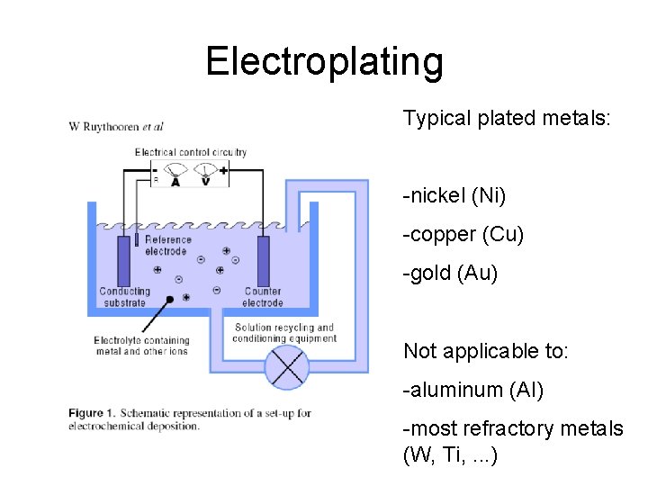
Electroplating Typical plated metals: -nickel (Ni) -copper (Cu) -gold (Au) Not applicable to: -aluminum (Al) -most refractory metals (W, Ti, . . . )

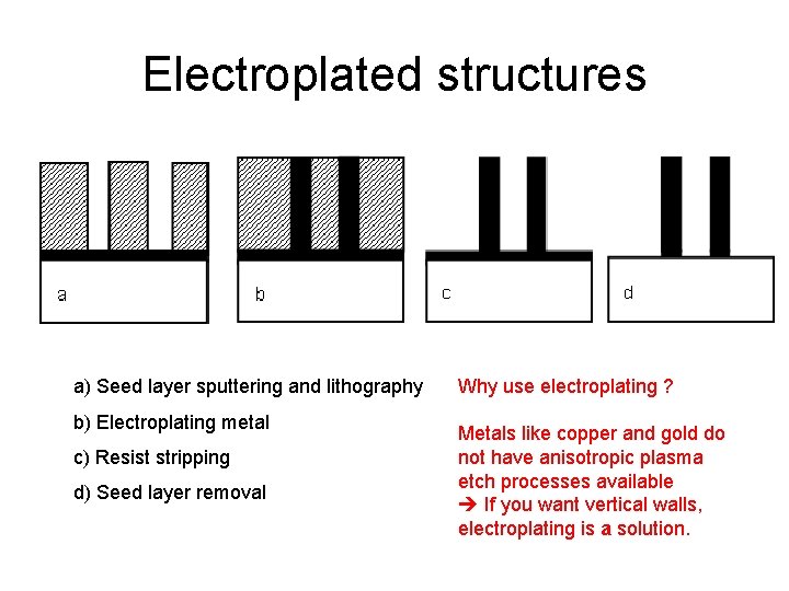
Electroplated structures a) Seed layer sputtering and lithography b) Electroplating metal c) Resist stripping d) Seed layer removal Why use electroplating ? Metals like copper and gold do not have anisotropic plasma etch processes available If you want vertical walls, electroplating is a solution.

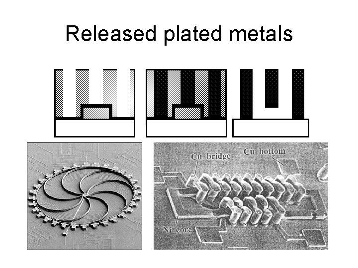
Released plated metals

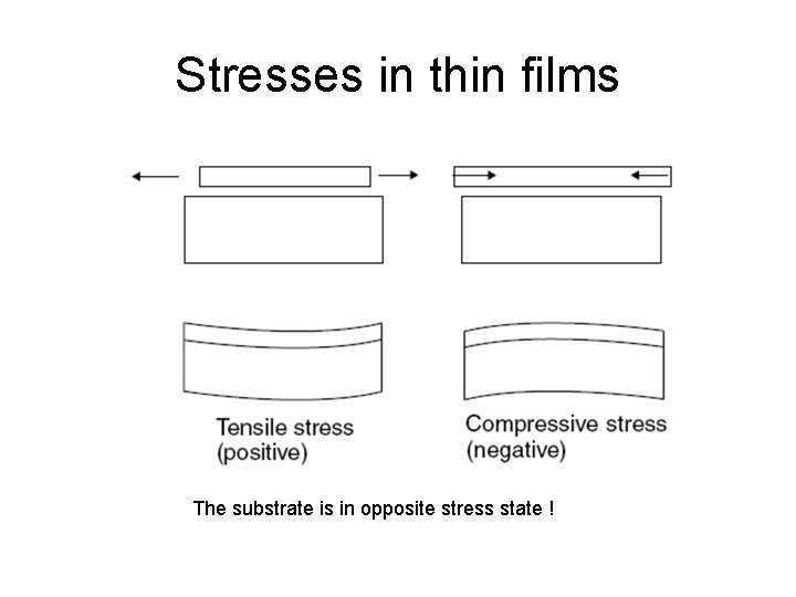
Stresses in thin films The substrate is in opposite stress state !

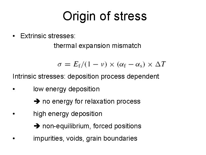
Origin of stress • Extrinsic stresses: thermal expansion mismatch Intrinsic stresses: deposition process dependent • low energy deposition no energy for relaxation process • high energy deposition non-equilibrium, forced positions • impurities, voids, grain boundaries

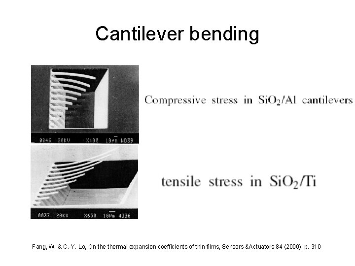
Cantilever bending Fang, W. & C. -Y. Lo, On thermal expansion coefficients of thin films, Sensors &Actuators 84 (2000), p. 310

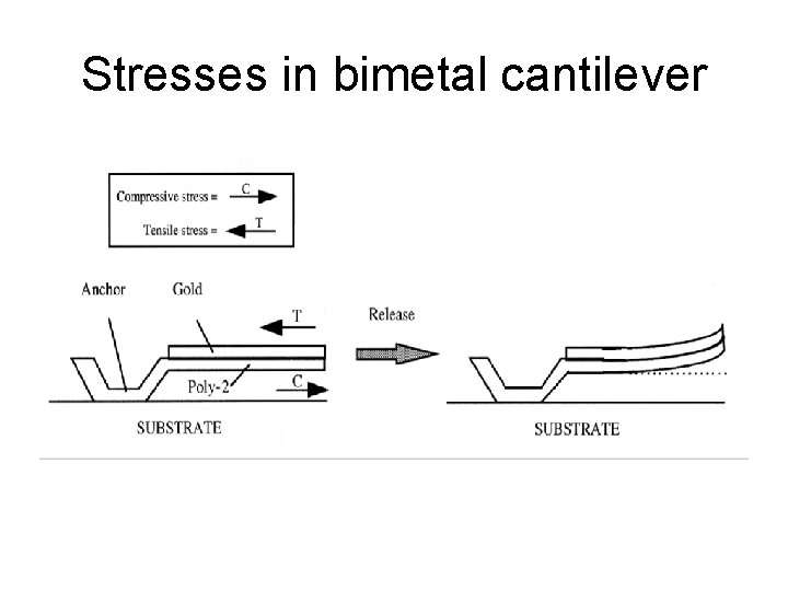
Stresses in bimetal cantilever

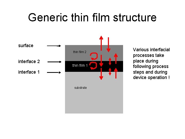
Generic thin film structure surface thin film 2 interface 2 thin film 1 interface 1 substrate Various interfacial processes take place during following process steps and during device operation !

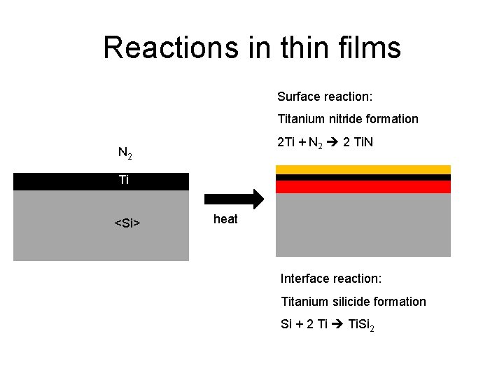
Reactions in thin films Surface reaction: Titanium nitride formation 2 Ti + N 2 2 Ti. N N 2 Ti <Si> heat Interface reaction: Titanium silicide formation Si + 2 Ti Ti. Si 2

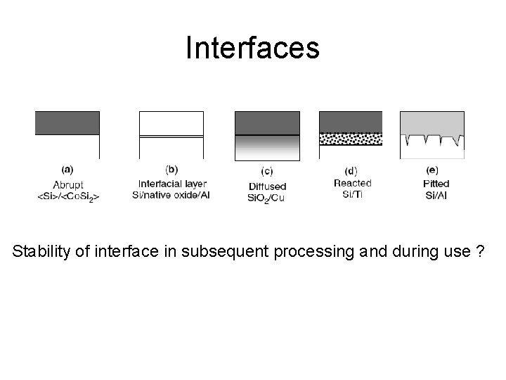
Interfaces Stability of interface in subsequent processing and during use ?

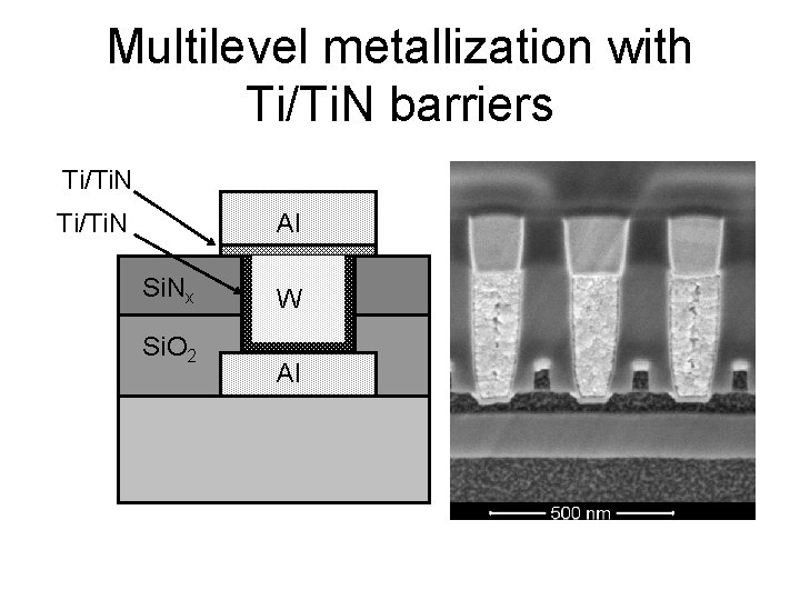
Barriers and adhesion layers In order to stabilize the interfaces, additional films are introduced: -to improve adhesion, e. g. Ti/Pt, Cr/Au -to prevent interdiffusion, Si/Ti. W/Al, Si. O 2/Ta. Nx/Cu; Si. O 2/Si. Nx/Cu -to prevent ion movement: glass/Al 2 O 3/poly-Si -to protect from ambient: Si. O 2/Si. Nx

Multilevel metallization with Ti/Ti. N barriers Ti/Ti. N Al Ti/Ti. N Si. Nx Si. O 2 W Al

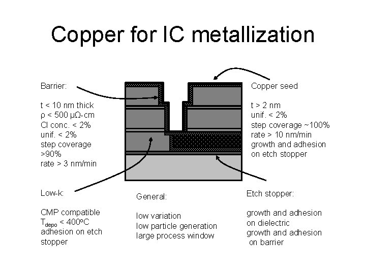
Copper for IC metallization Barrier: Copper seed t < 10 nm thick ρ < 500 µΩ-cm Cl conc. < 2% unif. < 2% step coverage >90% rate > 3 nm/min t > 2 nm unif. < 2% step coverage ~100% rate > 10 nm/min growth and adhesion on etch stopper Low-k: General: Etch stopper: CMP compatible Tdepo < 400 o. C adhesion on etch stopper low variation low particle generation large process window growth and adhesion on dielectric growth and adhesion on barrier

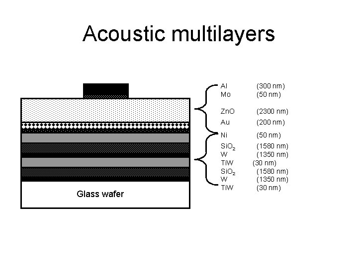
Acoustic multilayers Glass wafer Al Mo (300 nm) (50 nm) Zn. O (2300 nm) Au (200 nm) Ni (50 nm) Si. O 2 (1580 nm) W (1350 nm) Ti. W (30 nm) Si. O 2 (1580 nm) W (1350 nm) Ti. W (30 nm)

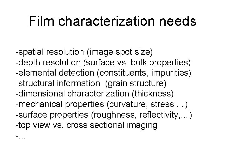
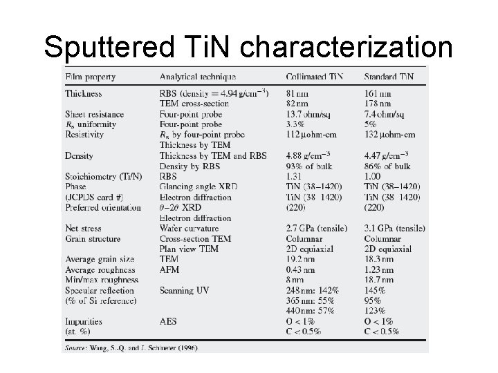
Film characterization needs -spatial resolution (image spot size) -depth resolution (surface vs. bulk properties) -elemental detection (constituents, impurities) -structural information (grain structure) -dimensional characterization (thickness) -mechanical properties (curvature, stress, …) -surface properties (roughness, reflectivity, …) -top view vs. cross sectional imaging -…

Sputtered Ti. N characterization

Thin films • On this course, we are interested in applications of thin films in microfabrication • Prof. Jari Koskinen is teaching Thin film technology (period IV): • “Principles of vacuum technology, surface physics and surface-ion interactions and low pressure plasma. Thin film methods: Physical vapor deposition, chemical vapor deposition, and other plasma. Characterization methods for thin films to determine, structure, composition, and mechanical and optical properties. ”