CVD Chemical Vapor Deposition sami franssilaaalto fi CVD
- Slides: 36

CVD Chemical Vapor Deposition sami. franssila@aalto. fi

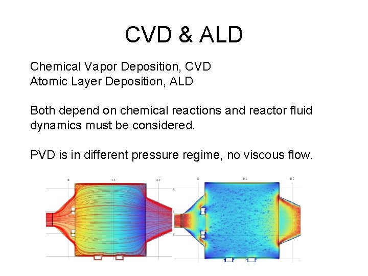
CVD & ALD Chemical Vapor Deposition, CVD Atomic Layer Deposition, ALD Both depend on chemical reactions and reactor fluid dynamics must be considered. PVD is in different pressure regime, no viscous flow.

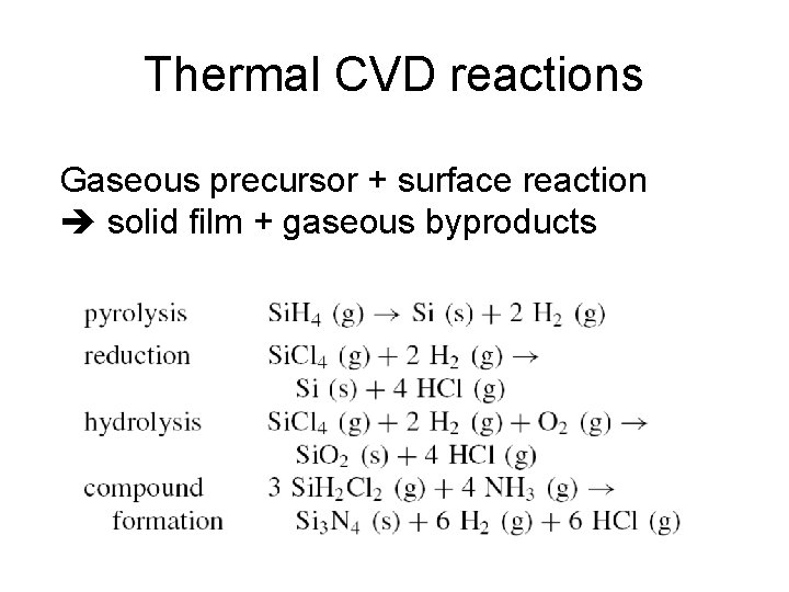
Thermal CVD reactions Gaseous precursor + surface reaction solid film + gaseous byproducts

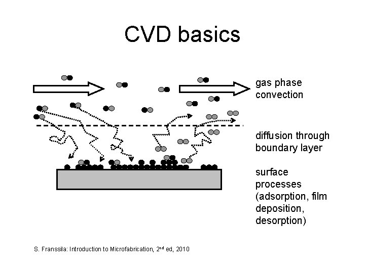
CVD basics gas phase convection diffusion through boundary layer surface processes (adsorption, film deposition, desorption) S. Franssila: Introduction to Microfabrication, 2 nd ed, 2010

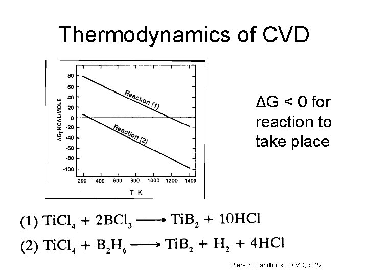
Thermodynamics of CVD ΔG < 0 for reaction to take place Pierson: Handbook of CVD, p. 22

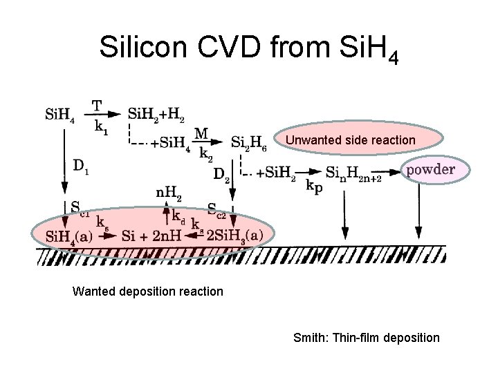
Silicon CVD from Si. H 4 Unwanted side reaction Wanted deposition reaction Smith: Thin-film deposition

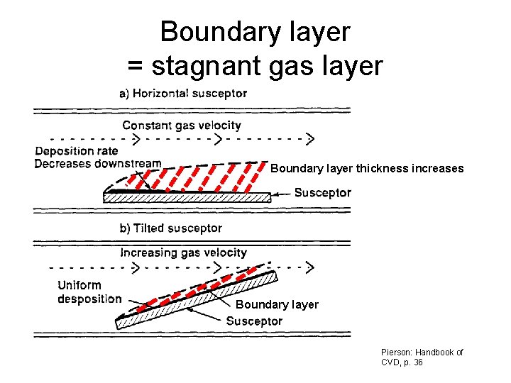
Boundary layer = stagnant gas layer Boundary layer thickness increases Boundary layer Pierson: Handbook of CVD, p. 36

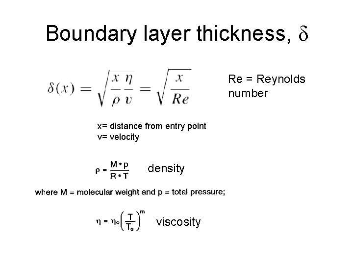
Boundary layer thickness, δ Re = Reynolds number x= distance from entry point v= velocity density viscosity

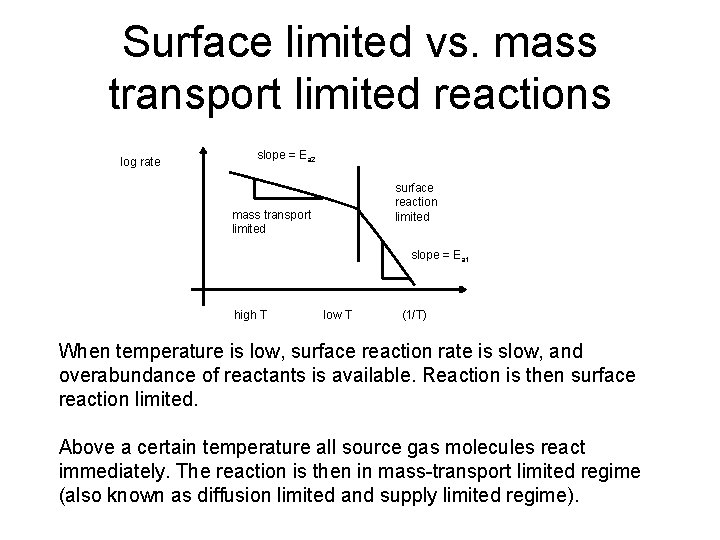
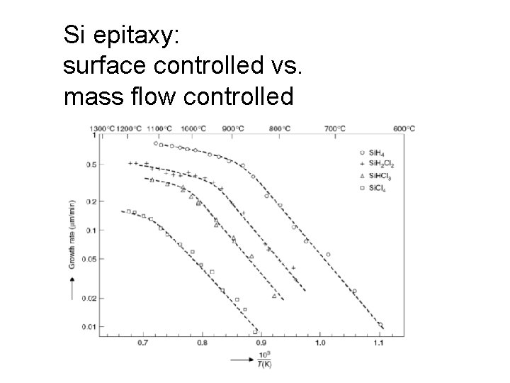
Surface limited vs. mass transport limited reactions log rate slope = Ea 2 surface reaction limited mass transport limited slope = Ea 1 high T low T (1/T) When temperature is low, surface reaction rate is slow, and overabundance of reactants is available. Reaction is then surface reaction limited. Above a certain temperature all source gas molecules react immediately. The reaction is then in mass-transport limited regime (also known as diffusion limited and supply limited regime).

Si epitaxy: surface controlled vs. mass flow controlled

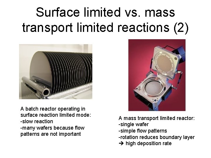
Surface limited vs. mass transport limited reactions (2) A batch reactor operating in surface reaction limited mode: -slow reaction -many wafers because flow patterns are not important A mass transport limited reactor: -single wafer -simple flow patterns -rotation reduces boundary layer high deposition rate

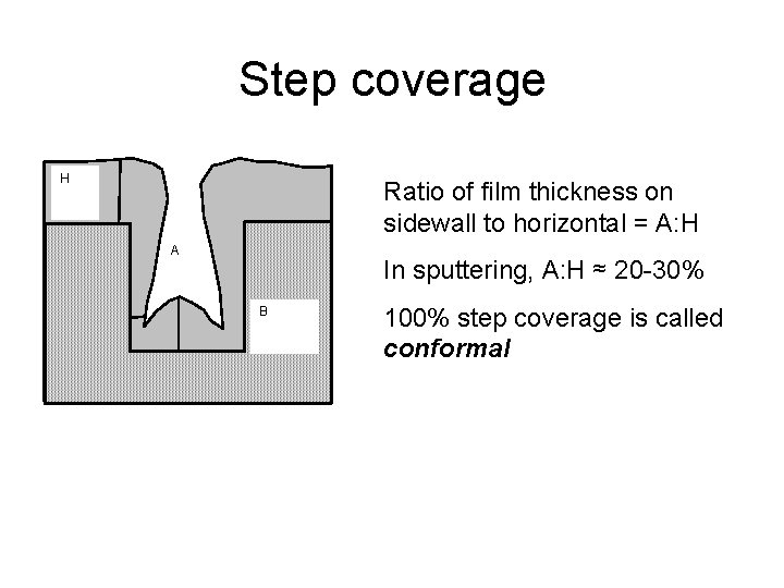
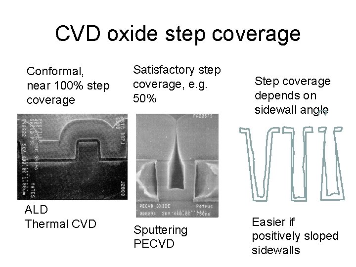
Step coverage H Ratio of film thickness on sidewall to horizontal = A: H A In sputtering, A: H ≈ 20 -30% B 100% step coverage is called conformal

CVD oxide step coverage Conformal, near 100% step coverage ALD Thermal CVD Satisfactory step coverage, e. g. 50% Sputtering PECVD Step coverage depends on sidewall angle Easier if positively sloped sidewalls

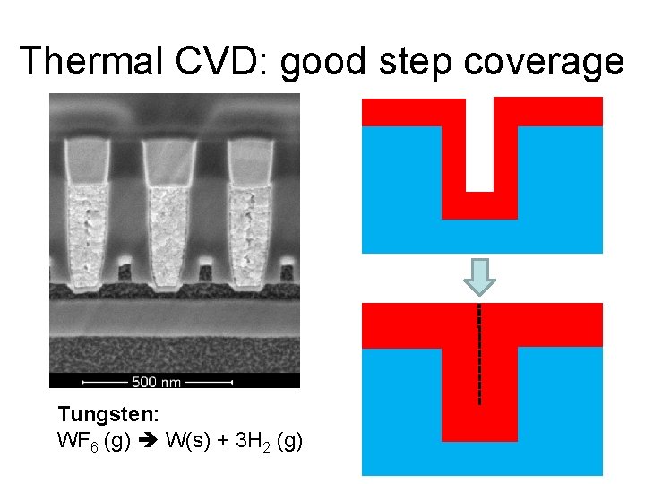
Thermal CVD: good step coverage Tungsten: WF 6 (g) W(s) + 3 H 2 (g)

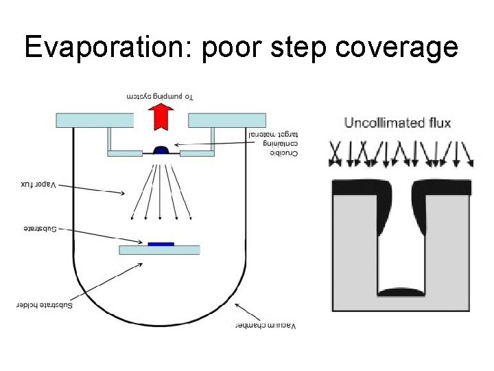
Evaporation: poor step coverage

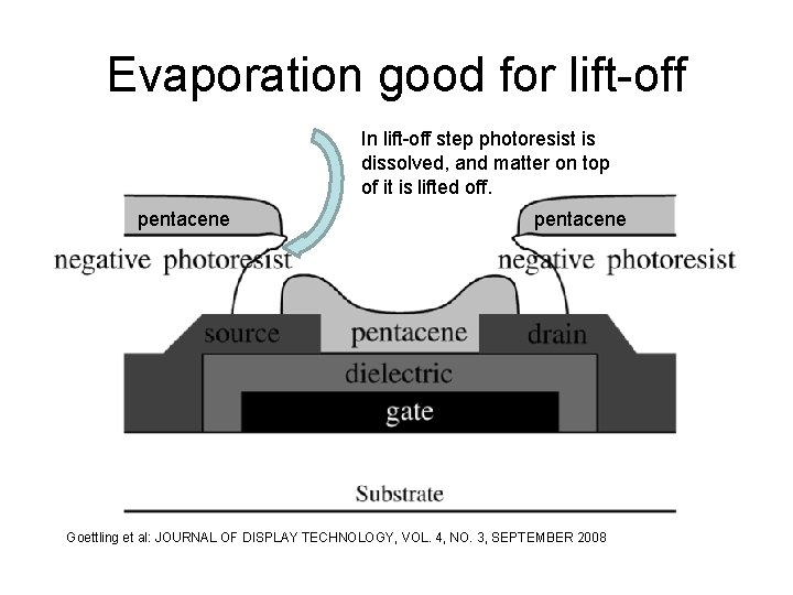
Evaporation good for lift-off In lift-off step photoresist is dissolved, and matter on top of it is lifted off. pentacene Goettling et al: JOURNAL OF DISPLAY TECHNOLOGY, VOL. 4, NO. 3, SEPTEMBER 2008

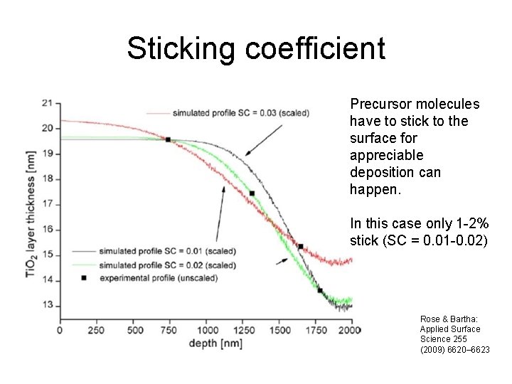
Sticking coefficient Precursor molecules have to stick to the surface for appreciable deposition can happen. In this case only 1 -2% stick (SC = 0. 01 -0. 02) Rose & Bartha: Applied Surface Science 255 (2009) 6620– 6623

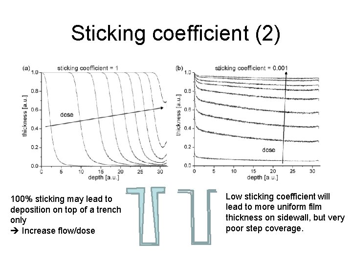
Sticking coefficient (2) 100% sticking may lead to deposition on top of a trench only Increase flow/dose Low sticking coefficient will lead to more uniform film thickness on sidewall, but very poor step coverage.

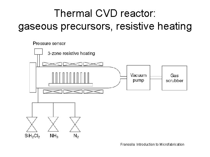
Thermal CVD reactor: gaseous precursors, resistive heating Franssila: Introduction to Microfabrication

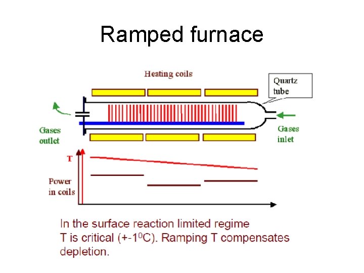
Ramped furnace

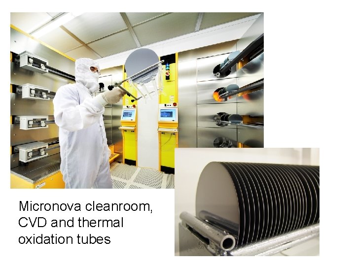
Micronova cleanroom, CVD and thermal oxidation tubes

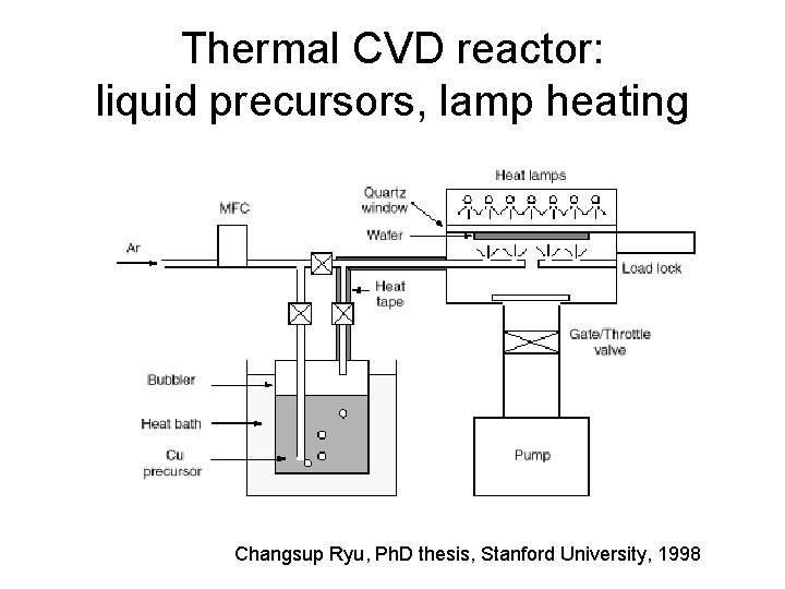
Thermal CVD reactor: liquid precursors, lamp heating Changsup Ryu, Ph. D thesis, Stanford University, 1998

LRP= Limited Reaction Processing • Very fast and powerful lamp heating • Introduce gases • Flash the lamp T up reaction • Pump away the gases • Introduce new gases • Flash the lamp T up reaction. . .

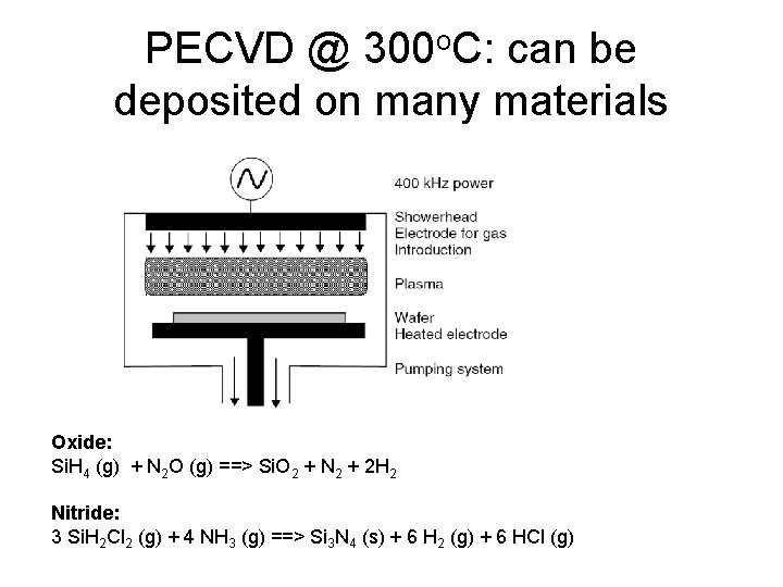
PECVD: Plasma Enhanced CVD • • Plasma aids in chemical reactions Can be done at low temperatures Wide deposition parameter range High rates (1 -10 nm/s) (thermal 10% of this)

PECVD @ 300 o. C: can be deposited on many materials Oxide: Si. H 4 (g) + N 2 O (g) ==> Si. O 2 + N 2 + 2 H 2 Nitride: 3 Si. H 2 Cl 2 (g) + 4 NH 3 (g) ==> Si 3 N 4 (s) + 6 H 2 (g) + 6 HCl (g)

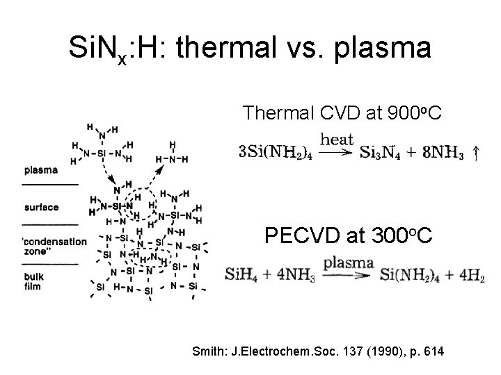
Si. Nx: H: thermal vs. plasma Thermal CVD at 900 o. C PECVD at 300 o. C Smith: J. Electrochem. Soc. 137 (1990), p. 614

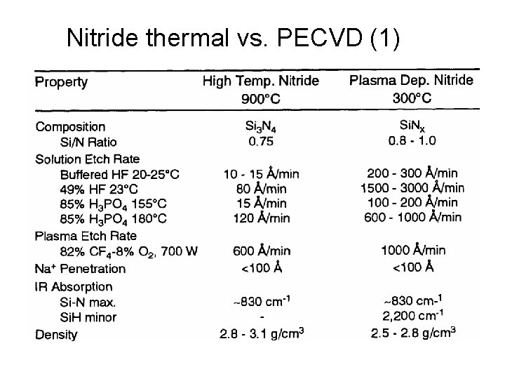
Nitride thermal vs. PECVD (1)

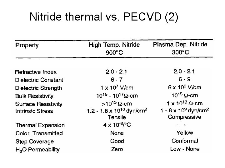
Nitride thermal vs. PECVD (2)

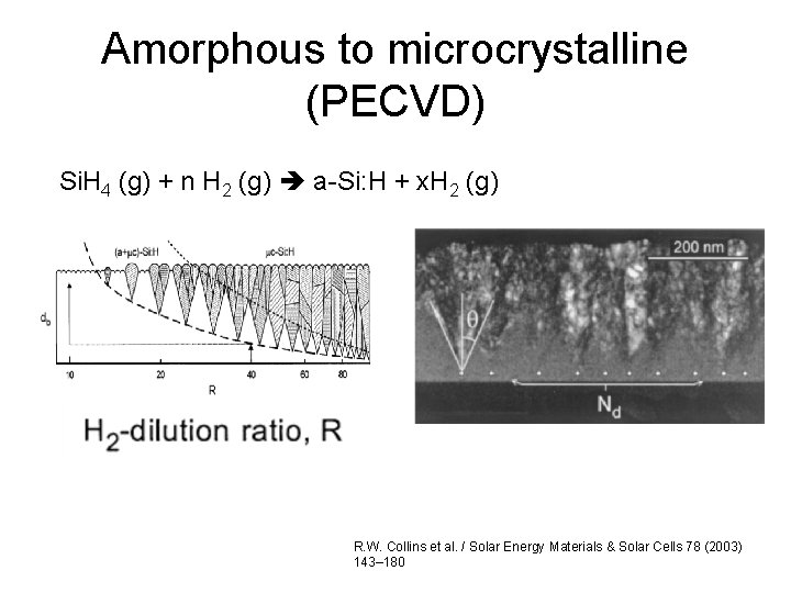
Amorphous to microcrystalline (PECVD) Si. H 4 (g) + n H 2 (g) a-Si: H + x. H 2 (g) R. W. Collins et al. / Solar Energy Materials & Solar Cells 78 (2003) 143– 180

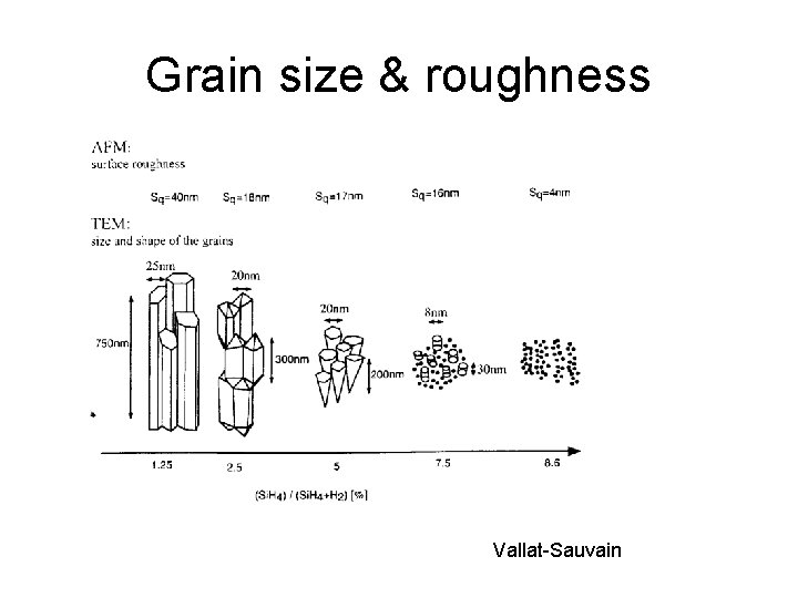
Grain size & roughness Vallat-Sauvain

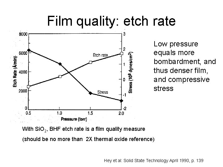
Film quality: etch rate Low pressure equals more bombardment, and thus denser film, and compressive stress With Si. O 2, BHF etch rate is a film quality measure (should be no more than 2 X thermal oxide reference) Hey et al: Solid State Technology April 1990, p. 139

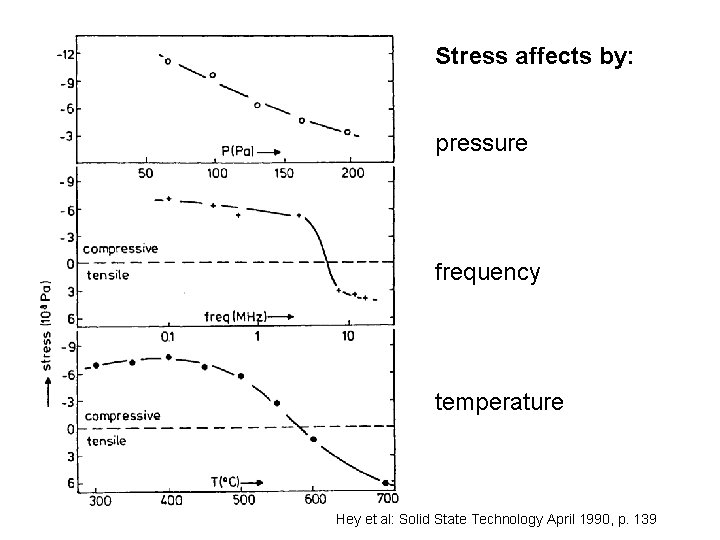
Stress affects by: pressure frequency temperature Hey et al: Solid State Technology April 1990, p. 139

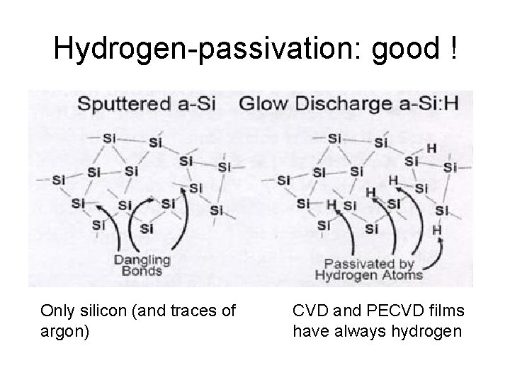
Hydrogen-passivation: good ! Only silicon (and traces of argon) CVD and PECVD films have always hydrogen

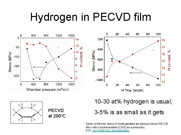
Hydrogen in PECVD film 10 -30 at% hydrogen is usual; PECVD at 200 o. C 3 -5% is as small as it gets Study of intrinsic stress in hydrogenated amorphous silicon PECVD films with cyclohexasilane (CHS) as a precursor, DOI: 10. 1109/PVSC. 2014. 6925582

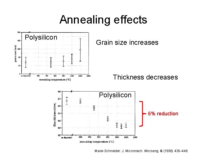
Annealing effects Polysilicon Grain size increases Thickness decreases Polysilicon 6% reduction Maier-Schneider: J. Micromech. Microeng. 6 (1996) 436– 446.

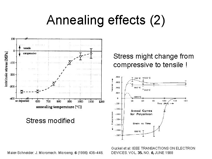
Annealing effects (2) Stress might change from compressive to tensile ! Stress modified Maier-Schneider: J. Micromech. Microeng. 6 (1996) 436– 446. Guckel et al: IEEE TRANSACTIONS ON ELECTRON DEVICES. VOL. 35. NO. 6, JUNE 1988