Scaling sami franssilaaalto fi Contents Wafer size scaling


 wafer load/unload time")


 =")

 does NOT scale; it")


- Slides: 41
Scaling sami. franssila@aalto. fi
Contents Wafer size scaling Chip size scaling Wafer thickness scaling Projection lithography scaling Cost savings scaling with wafer size Etch scaling (from wet to dry) Etch selectivity scaling (CMOS gate) Film thickness scaling (MLM, constant AR) Fab size scaling Fab cost scaling
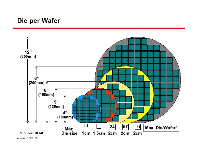
Wafer size scaling 525 µm 625 µm 775 µm ? ? 925 µm Wafer thickness scaling
Wafer specifications for CMOS Wafer size 100 125 150 200 300 mm Thickness TTV Warp Flatness 525 675 725 775 µm 3 3 2 1. 5 1 µm 20 -30 18 -35 20 -30 10 -20 µm <3 <2 <1 0. 5 -0. 8 µm Oxygen OISF 20 17 15 14 12 pmma 100 -200 100 <10 none cm-2 Particles Particle size 10 10 5 -10 10 -100 50 -100 #/wafer 0. 3 0. 16 0. 12 µm Metals 1012 1011 5*1010 109 atoms/cm 2
Useful chips & edge exclusion
100 mm vs. 150 mm 10*10 mm chip Area ratio = 2. 25: 1 but chip number ratio is 2. 6: 1
200 mm vs. 300 mm 20*30 mm chip size Chip number ratio 2. 6: 1 http: //www. silicon-edge. co. uk/j/index. php/resources/die-per-wafer
Yield & LW If LW is scaled by factor 0. 7 Then area A is scaled by factor of 0. 5 Defect density D = 0. 01 cm-2 Chip original size 50 mm 2 Yoriginal = exp (-50*0. 01) = 60% Y scaled = exp (-25*0. 01) = 78%
Chip shrink & larger wafers Smaller linewidth smaller chip size less probably defective yield going up Same chip size more fit on a larger wafer & less edge effects more chips/wafer
Chip size vs. Yield Good Money chips USD 255 1020 98 1176 32 1696 18 1314 10 1490 6 1632 4 1668 EE 141 © Digital Integrated Circuits 2 nd Introduction 1 Digital Integrated Circuits A Design Perspective Introduction Jan M. Rabaey Anantha Chandrakasan.
Wafer size and demand Doering, R. & Y. Nishi: Limits of integrated circuit manufacturing, Proc. IEEE Vol. 89 (2001) p. 375
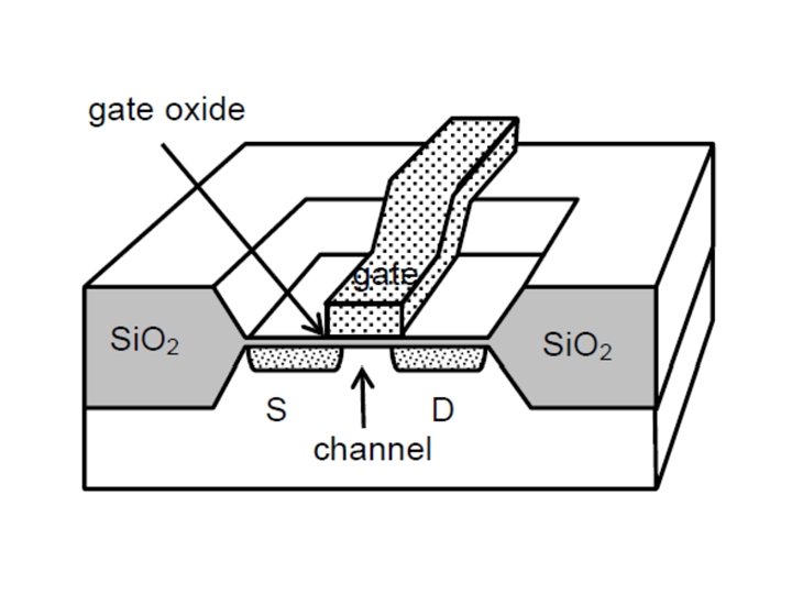
Optical projection lithography Sources of radiation (UV 365 nm-436 nm, DUV 193 nm-248 nm, EUV, X-rays, electrons, ions) Optical system I (lenses, mirrors) Mask (pattern) Optical system II (lenses, mirrors) Numerical aperture NA=sin Imaging medium (resist) Wafer (with patterns) Wafer stage (alignment mechanism)
Projection litho performance
Table 10. 1: Linewidth scaling of CMOS Wavelength Aperture k factor =436 nm NA=0. 38 k 1=0. 8 =365 nm NA=0. 48 k 1=0. 6 =248 nm NA=0. 60 k 1=0. 6 =248 nm NA=0. 65 k 1=0. 5 Linewidth Do. F 1 µm 0. 5 µm 0. 25 µm 0. 18 µm 1. 5µm 0. 8 µm 0. 35 µm 0. 30 µm Because depth of focus (Do. F) gets smaller, CMP planarization becomes more important all the time.
Projection lithography scaling Lin, MEMS 2010
Reduction stepper: 100 exposures/wafer Compared to proximity litho: -much slower -smaller LW possible -better alignment Nikon. com
Reduction factor, often 5 X Mask 1 µm minimum linewidth 5 X optical reduction 0. 2 µm on wafer Mask making becomes much easier and more economical.
Photomask cost scaling Min LW Cost 3 µm 1 µm 300 euros 500 euros 1000 euros, quality checked Mask LW Wafer LW Cost 1 µm 0. 5 µm 200 nm 100 nm 0. 2 µm 0. 1 µm 40 nm 2000 euros 5000 euros 20000 euros 50000 euros 1 X litho 5 X reduction litho For a 40 mask microprocessor mask set costs $2 M
New prediction of wafer sizes https: //www. extremetech. com/extreme/163372 -atom-everywhere-intelbreaks-ground-on-first-450 mm-fab 2013
Making 450 mm etcher Maximum throughput of an etch tool is governed by two basic factors: 1) wafer load/unload time 2) etch time. With good engineering wafer throughput is independent of wafer size, so that chip throughput improves as the wafer size increases. But “good engineering” is not free, and it takes work to keep the etch uniformity the same for a larger wafer. The larger etch tools also cost more money to make. But if the tool cost does not increase as fast as the wafer area, the result is a lower cost per chip. This is the goal, and the reason why we pursue larger wafer sizes. Chris Mack: http: //www. lithoguru. com/scientist/essays/why 450. html
Cost analysis of 450 mm etcher Wafer diameter increase of 1. 5 X Wafer area increases by factor of 2. 25 Because edge die effect it is possible for the number of good chips to increase at a slightly higher amount, maybe up to a factor of 2. 4. If the cost of the etcher, the amount of fab floor space, and the per -wafer cost of process chemicals all increase by 30%, the cost per chip will change by 1. 3/2. 25 = 0. 58. Thus, the etch cost per chip will be 42% lower.
450 mm lithography Reduction stepper litho process time consists of: 1) wafer load/unload time 2) Exposure time The load time can be kept constant as a function of wafer size, but the exposure time increases as the wafer size increases. And since wafer load/unload time is a very small fraction of the total process time, the result for lithography is a near-constant wafer-area throughput (rather than the constant wafer throughput for etch) as wafer size is changed. Proportion of lithography of total costs will increase. Today 50%
Latest predictions 450 mm Officially On Hold… January 17, 2017 Is 450 mm over? Not for good. At some point, technology, market, and the resulting economic changes will inevitability bring the discussion, and likely, the development, back. However, the New York-based, 450 mm global consortium, G 450 C is done.
Refresher: etch profiles Wet etching isotropic profile Plasma etching anisotropic profile
Wet etched profile: 1 µm thick film 5 µm 3 µm 2 µm 1 µm
Plasma etched profile: 1 µm film 5 µm 3 µm 2 µm 1 µm
Wet etched profile: 200 nm film 5 µm 3 µm 2 µm 1 µm
Plasma etched profile: 200 nm film 5 µm 3 µm 2 µm 1 µm
Etchback Conformal deposition Anisotropic etch 200 nm/min for 1 minute. 200 nm 400 nm
Etch time, end point and overetch 300 nm 100 % conformal deposition. 200 nm Etch rate 100 nm/min. Anisotropic etch. Etch time 1 min. 200 nm high spacers formed Etch time 3 minutes; i. e. 2 minutes overetch (200%). Clears spacers.
Spacers Stop etching here and leave the spacers ! Will be useful in CMOS scaling.
CMOS gate etch selectivity CMOS linewidth: 5 µm Polysilicon gate: 500 nm thick Gate oxide thickness (LW/50) = 100 nm Etch selectivity poly: oxide = 10: 1 Overetch = 50 % Oxide loss = nm Oxide loss = % of original thickness CMOS linewidth: 1 µm Polysilicon gate: 300 nm thick Gate oxide thickness (LW/50) = 20 nm Overetch = 50 % Oxide loss = same % loss as in above, Calculate etch selectivity poly: oxide needed to achieve this !
CMOS linewidth: 5 µm Polysilicon gate: 500 nm thick Gate oxide thickness (LW/50) = 100 nm Etch selectivity poly: oxide = 10: 1 Presume: 500 nm/min poly 50 nm/min oxide Overetch = 50 % 0. 5 min oxide etched Oxide loss = 25 nm Oxide loss = 25% of original thickness CMOS linewidth: 1 µm Polysilicon gate: 300 nm thick Gate oxide thickness (LW/50) = 20 nm Overetch = 50 % Oxide loss = same % loss as in above, Calculate etch selectivity poly: oxide needed! Presume 300 nm/min 50% oe is 30 secs 5 nm loss allowed 10 nm/min oxide rate 30: 1 selectivity needed
Schematic cross section CMP Grenoble
Aspect ratio scaling, real SEM Actually, aspect ratio (height: width) does NOT scale; it has remained more or less 1: 1 for decades. IBM
8 -level IC metallization
Fab cost scaling 1957 1967 1977 1987 1997 2007 2017 0. 2 M$ 2. 5 M$ 1000 M$ 3000 M$ 6000 M$
Fab size scaling Year Wafer size LW WPM* 1970 1980 1990 2000 2010 2020 3” 100 mm 150 mm 200 mm 300 mm 10 µm 2 µm 0. 8 µm 0. 18 µm 32 nm 11 nm 1000 5000 10000 20000 50000 70000 * Wafer starts per month
How many fabs in the world ? IC industry 300 B$ Let’s assume it is 200 mm wafers only (=300 cm 2/wafer) Cost of processed silicon is 5 $/cm 2 In order to produce 300 B$ 6*1010 cm 2 200 M wafers One 200 mm fab produces 20 000 wafers/month = 200 000/year 1000 fabs (order of magnitude only: 500 more real)