Thin films sami franssilaaalto fi 1 D 2
- Slides: 51

Thin films sami. franssila@aalto. fi

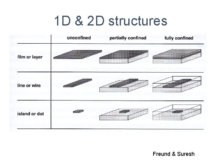
1 D & 2 D structures Freund & Suresh

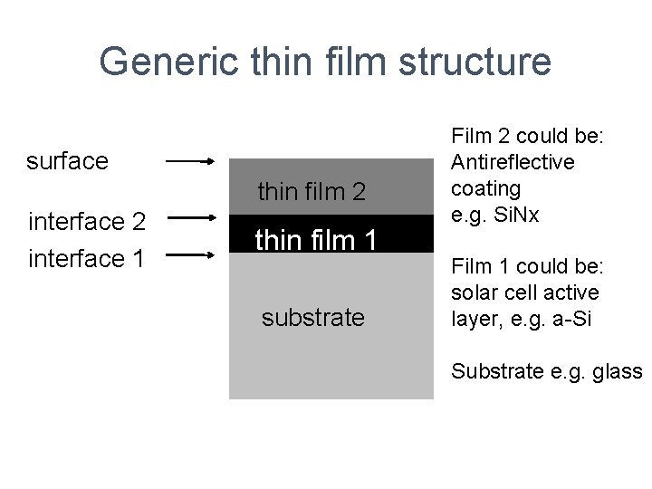
Generic thin film structure surface thin film 2 interface 1 thin film 1 substrate Film 2 could be: Antireflective coating e. g. Si. Nx Film 1 could be: solar cell active layer, e. g. a-Si Substrate e. g. glass

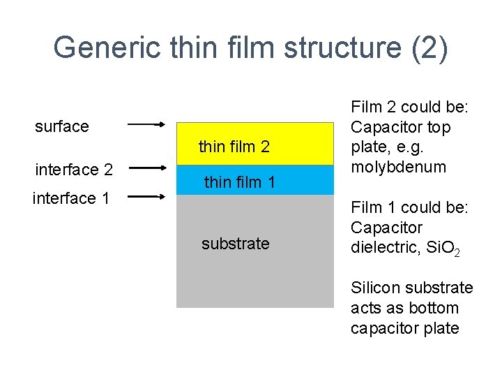
Generic thin film structure (2) surface thin film 2 interface 1 thin film 1 substrate Film 2 could be: Capacitor top plate, e. g. molybdenum Film 1 could be: Capacitor dielectric, Si. O 2 Silicon substrate acts as bottom capacitor plate

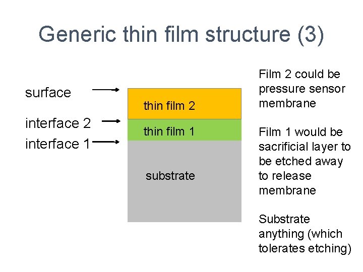
Generic thin film structure (3) surface interface 2 interface 1 thin film 2 thin film 1 substrate Film 2 could be pressure sensor membrane Film 1 would be sacrificial layer to be etched away to release membrane Substrate anything (which tolerates etching)

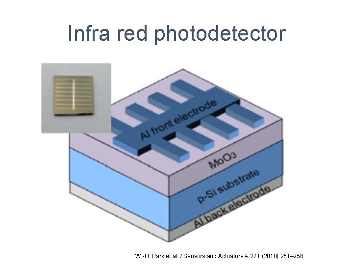
Infra red photodetector W. -H. Park et al. / Sensors and Actuators A 271 (2018) 251– 256

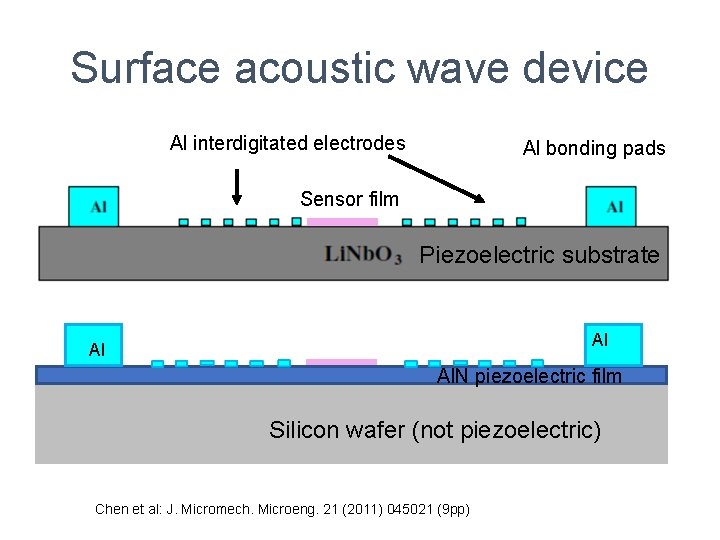
Surface acoustic wave device Al interdigitated electrodes Al bonding pads Sensor film Piezoelectric substrate Al Al Al. N piezoelectric film Silicon wafer (not piezoelectric) Chen et al: J. Micromech. Microeng. 21 (2011) 045021 (9 pp)

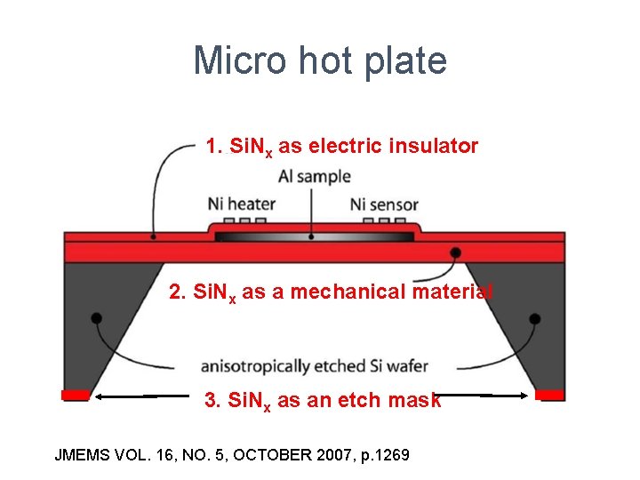
Micro hot plate 1. Si. Nx as electric insulator 2. Si. Nx as a mechanical material 3. Si. Nx as an etch mask JMEMS VOL. 16, NO. 5, OCTOBER 2007, p. 1269

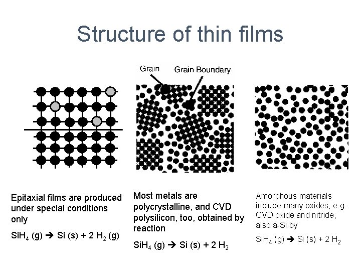
Structure of thin films Epitaxial films are produced under special conditions only Si. H 4 (g) Si (s) + 2 H 2 (g) Most metals are polycrystalline, and CVD polysilicon, too, obtained by reaction Si. H 4 (g) Si (s) + 2 H 2 Amorphous materials include many oxides, e. g. CVD oxide and nitride, also a-Si by Si. H 4 (g) Si (s) + 2 H 2

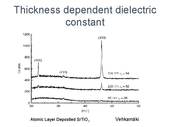
Thin films vs. bulk Properties different from bulk materials – Density – Resistivity – Thermal conductivity – Refractive index – Dielectric constant –… Properties & structure thickness dependent

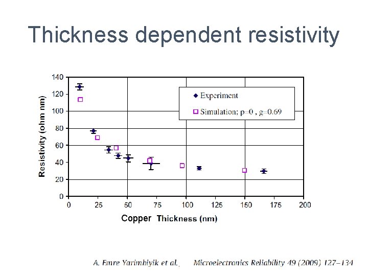
Thickness dependent resistivity Copper

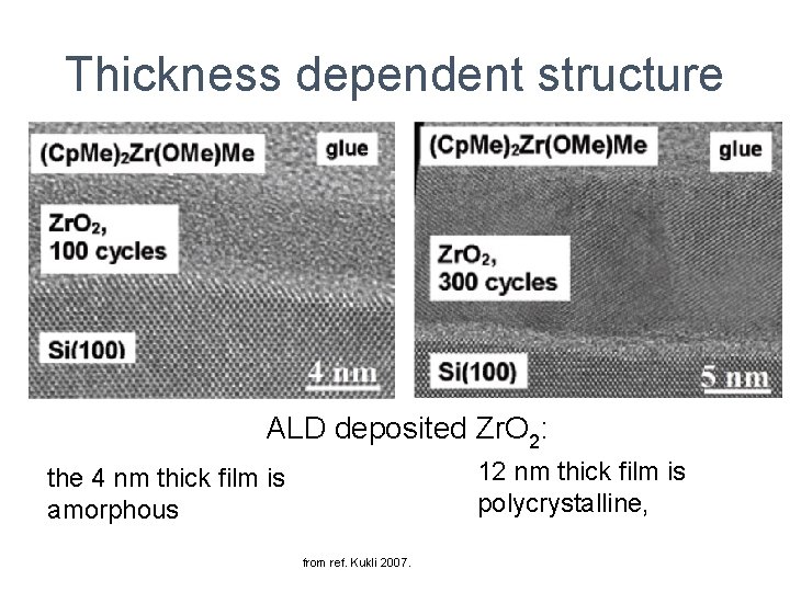
Thickness dependent structure ALD deposited Zr. O 2: 12 nm thick film is polycrystalline, the 4 nm thick film is amorphous from ref. Kukli 2007.

Thickness dependent dielectric constant Atomic Layer Deposited Sr. Ti. O 3 Vehkamäki

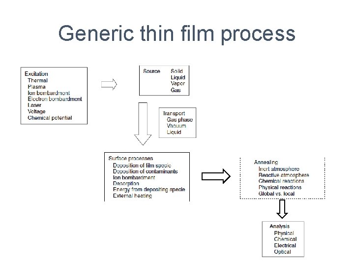
Generic thin film process

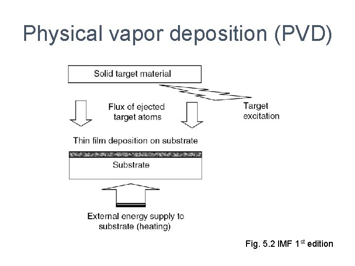
Physical vapor deposition (PVD) Fig. 5. 2 IMF 1 st edition

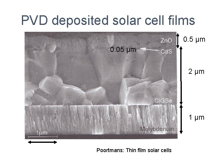
PVD deposited solar cell films 0. 5 µm 0. 05 µm 2 µm 1 µm Poortmans: Thin film solar cells

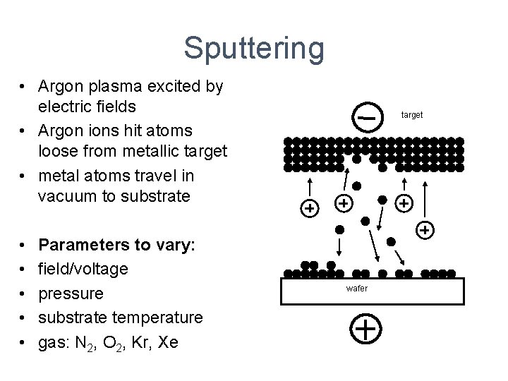
Sputtering • Argon plasma excited by electric fields • Argon ions hit atoms loose from metallic target • metal atoms travel in vacuum to substrate • • • Parameters to vary: field/voltage pressure substrate temperature gas: N 2, O 2, Kr, Xe target wafer

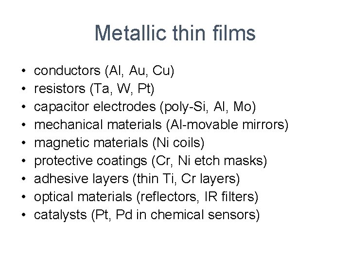
Metallic thin films • • • conductors (Al, Au, Cu) resistors (Ta, W, Pt) capacitor electrodes (poly-Si, Al, Mo) mechanical materials (Al-movable mirrors) magnetic materials (Ni coils) protective coatings (Cr, Ni etch masks) adhesive layers (thin Ti, Cr layers) optical materials (reflectors, IR filters) catalysts (Pt, Pd in chemical sensors)

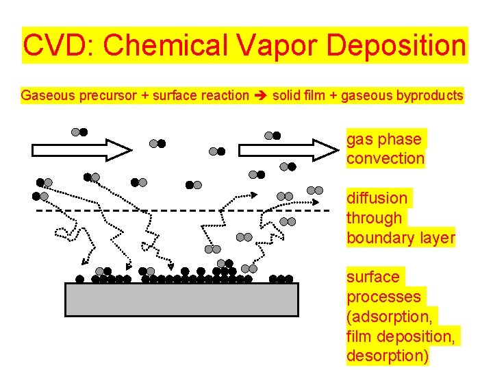
CVD: Chemical Vapor Deposition Gaseous precursor + surface reaction solid film + gaseous byproducts gas phase convection diffusion through boundary layer surface processes (adsorption, film deposition, desorption)

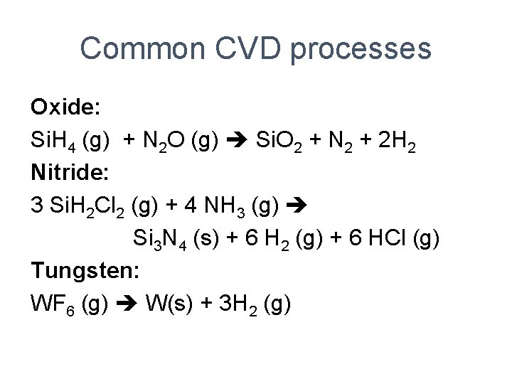
Common CVD processes Oxide: Si. H 4 (g) + N 2 O (g) Si. O 2 + N 2 + 2 H 2 Nitride: 3 Si. H 2 Cl 2 (g) + 4 NH 3 (g) Si 3 N 4 (s) + 6 H 2 (g) + 6 HCl (g) Tungsten: WF 6 (g) W(s) + 3 H 2 (g)

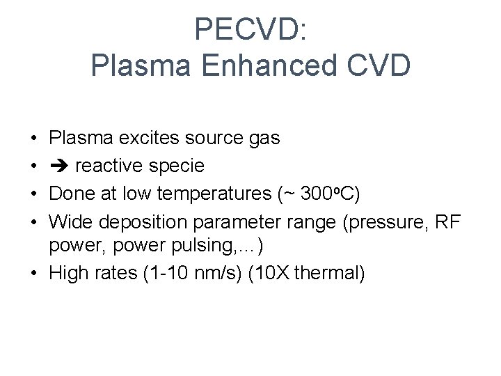
PECVD: Plasma Enhanced CVD • • Plasma excites source gas reactive specie Done at low temperatures (~ 300 o. C) Wide deposition parameter range (pressure, RF power, power pulsing, …) • High rates (1 -10 nm/s) (10 X thermal)

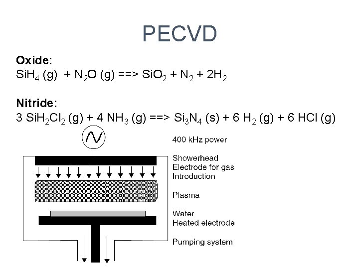
PECVD Oxide: Si. H 4 (g) + N 2 O (g) ==> Si. O 2 + N 2 + 2 H 2 Nitride: 3 Si. H 2 Cl 2 (g) + 4 NH 3 (g) ==> Si 3 N 4 (s) + 6 H 2 (g) + 6 HCl (g)

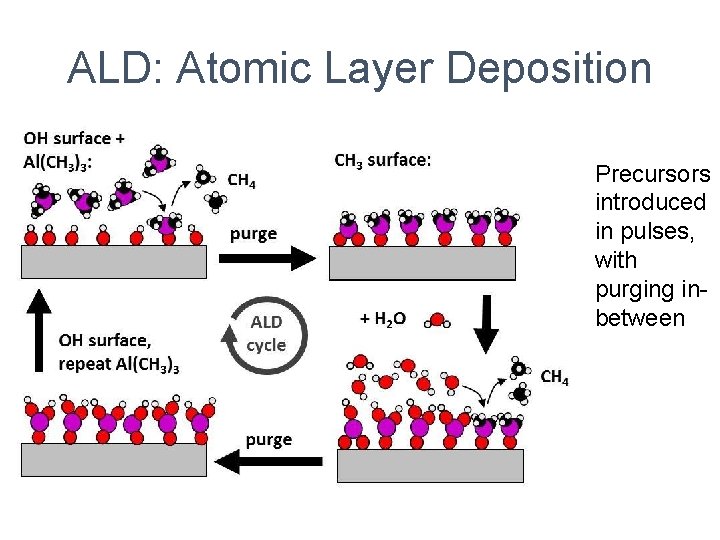
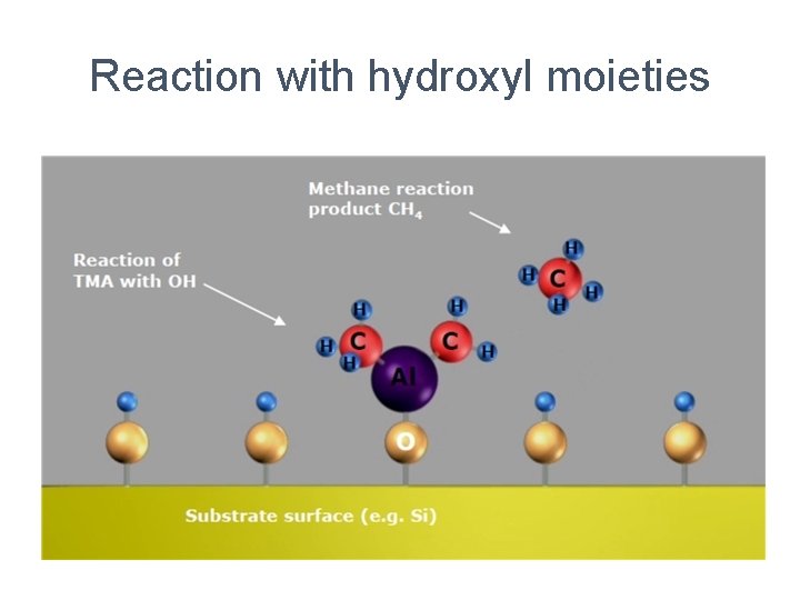
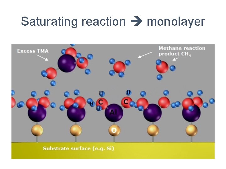
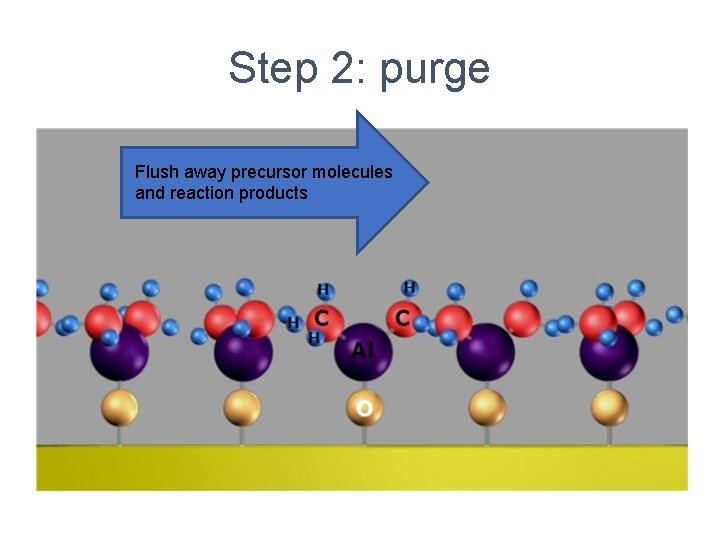
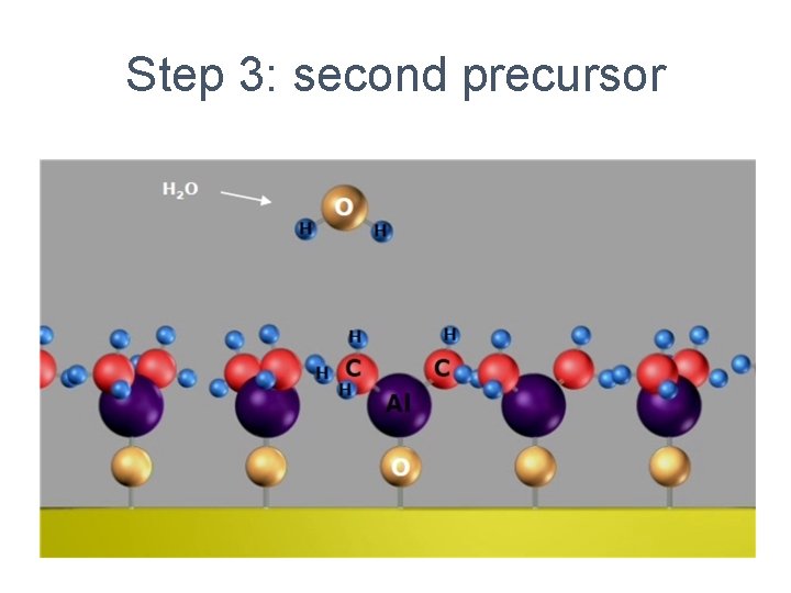
ALD: Atomic Layer Deposition Precursors introduced in pulses, with purging inbetween

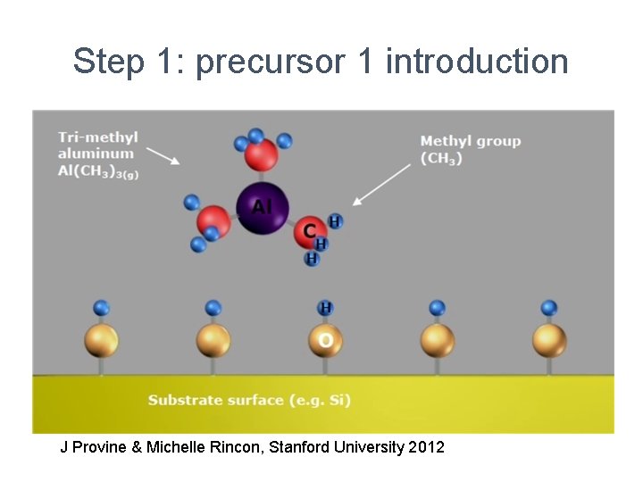
Step 1: precursor 1 introduction J Provine & Michelle Rincon, Stanford University 2012

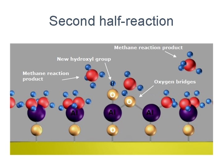
Reaction with hydroxyl moieties

Saturating reaction monolayer

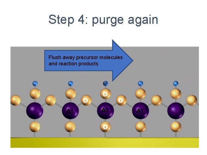
Step 2: purge Flush away precursor molecules and reaction products

Step 3: second precursor

Second half-reaction

Step 4: purge again Flush away precursor molecules and reaction products

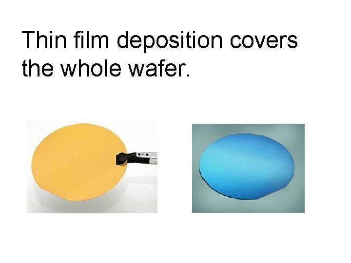
Thin film deposition covers the whole wafer.

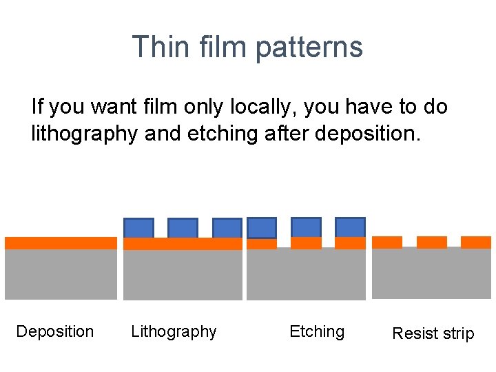
Thin film patterns If you want film only locally, you have to do lithography and etching after deposition. Deposition Lithography Etching Resist strip

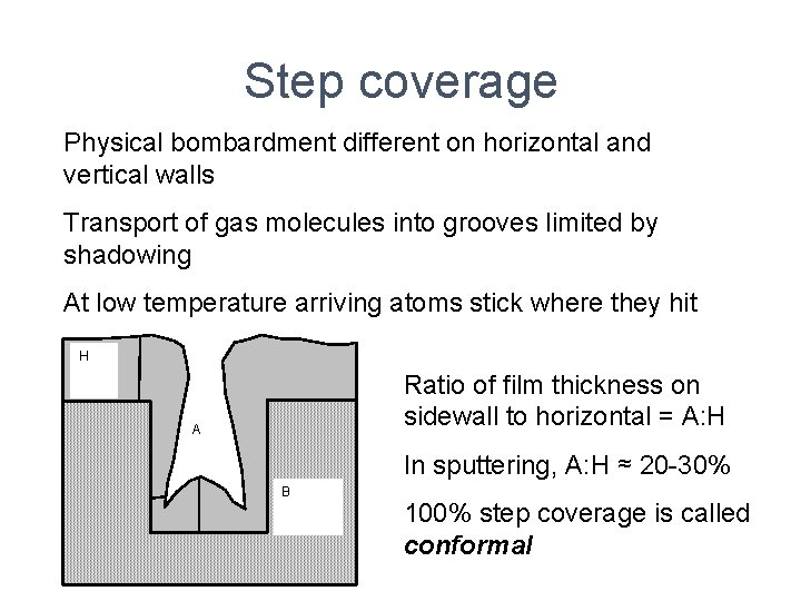
Step coverage Physical bombardment different on horizontal and vertical walls Transport of gas molecules into grooves limited by shadowing At low temperature arriving atoms stick where they hit H Ratio of film thickness on sidewall to horizontal = A: H A In sputtering, A: H ≈ 20 -30% B 100% step coverage is called conformal

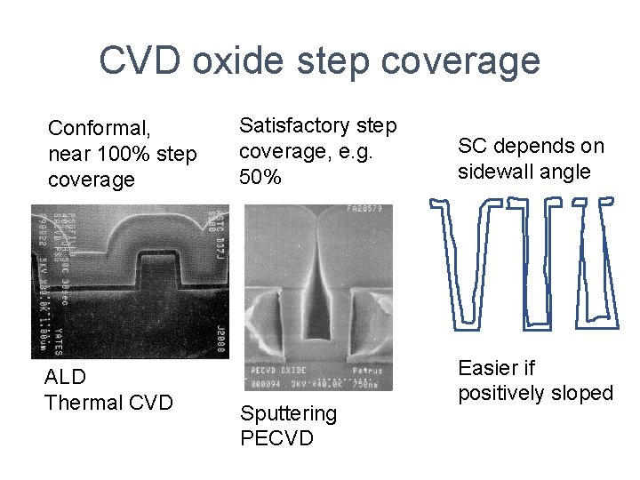
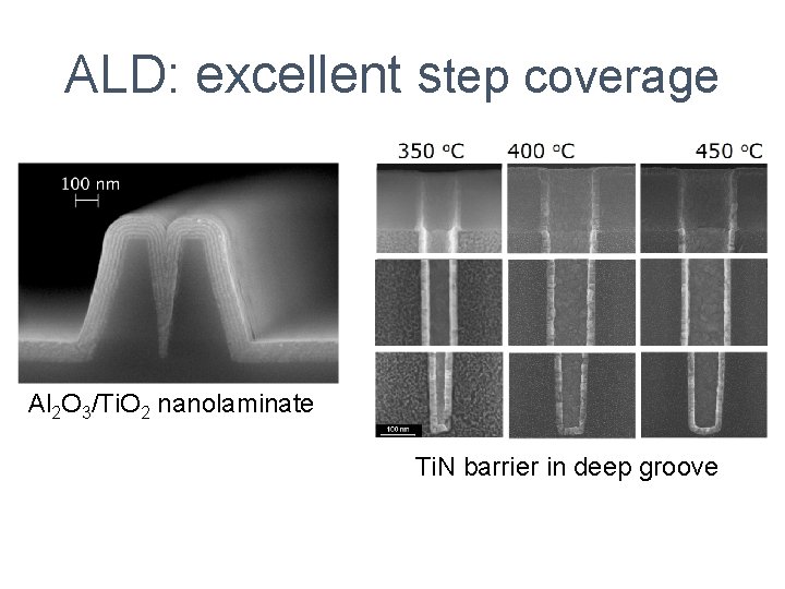
CVD oxide step coverage Conformal, near 100% step coverage ALD Thermal CVD Satisfactory step coverage, e. g. 50% Sputtering PECVD SC depends on sidewall angle Easier if positively sloped

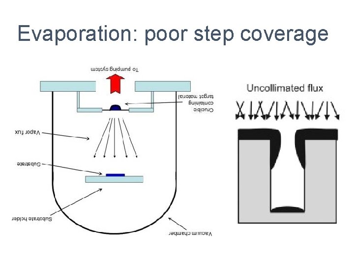
Evaporation: poor step coverage

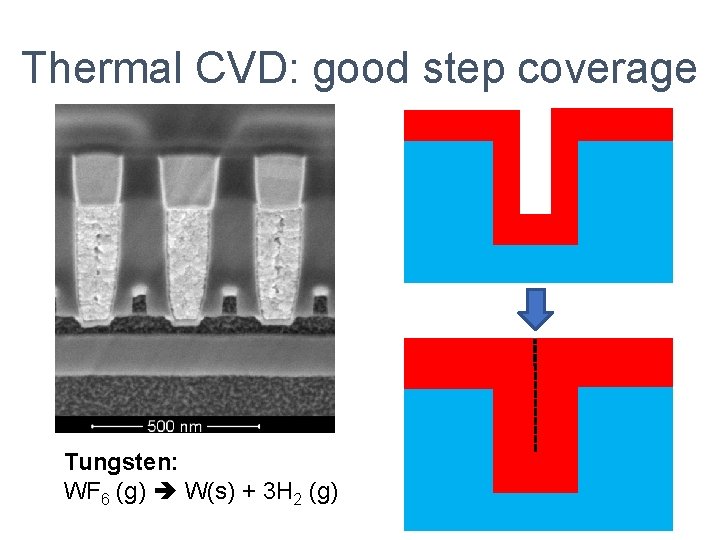
Thermal CVD: good step coverage Tungsten: WF 6 (g) W(s) + 3 H 2 (g)

ALD: excellent step coverage Al 2 O 3/Ti. O 2 nanolaminate Ti. N barrier in deep groove

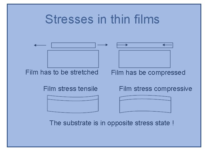
Stresses in thin films Film has to be stretched Film stress tensile Film has be compressed Film stress compressive The substrate is in opposite stress state !

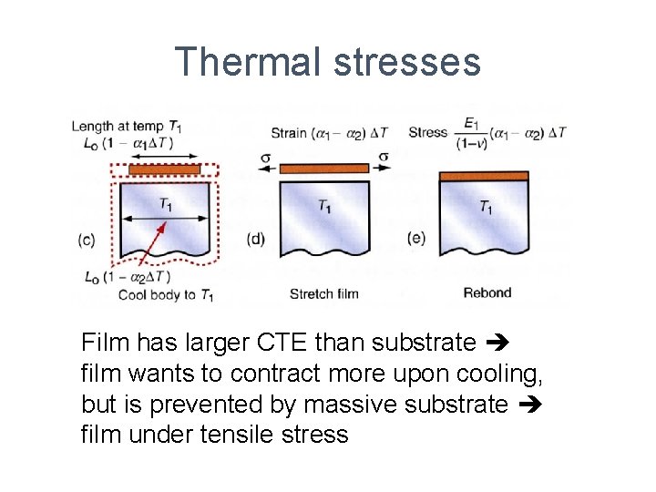
Thermal stresses Film has larger CTE than substrate film wants to contract more upon cooling, but is prevented by massive substrate film under tensile stress

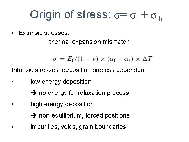
Origin of stress: σ= σi + σth • Extrinsic stresses: thermal expansion mismatch Intrinsic stresses: deposition process dependent • low energy deposition no energy for relaxation process • high energy deposition non-equilibrium, forced positions • impurities, voids, grain boundaries

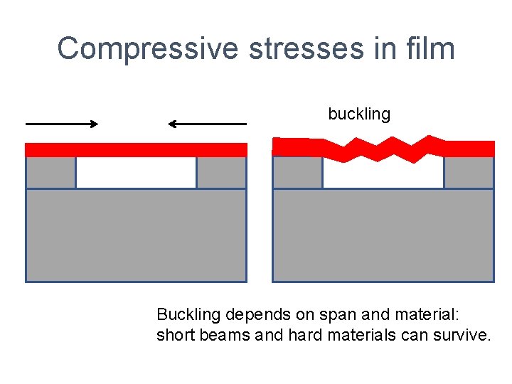
Compressive stresses in film buckling Buckling depends on span and material: short beams and hard materials can survive.

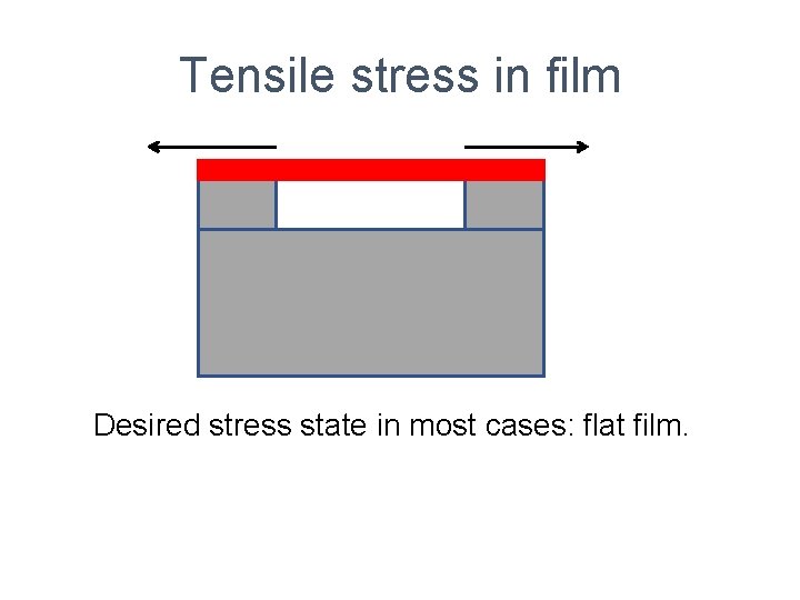
Tensile stress in film Desired stress state in most cases: flat film.

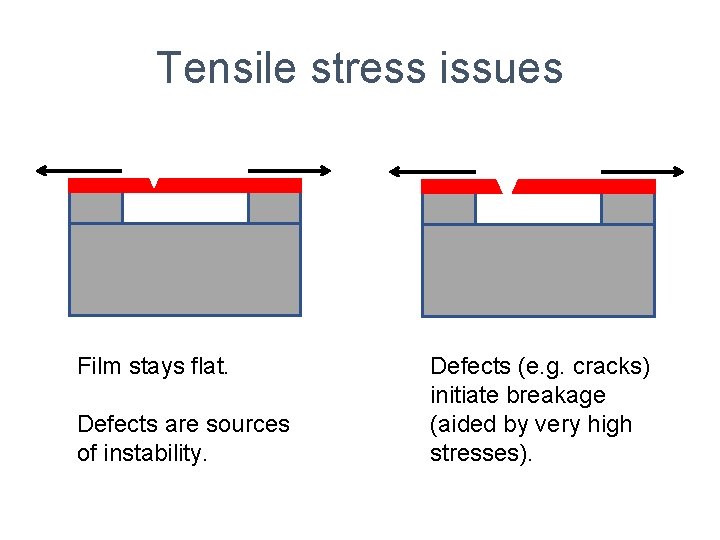
Tensile stress issues Film stays flat. Defects are sources of instability. Defects (e. g. cracks) initiate breakage (aided by very high stresses).

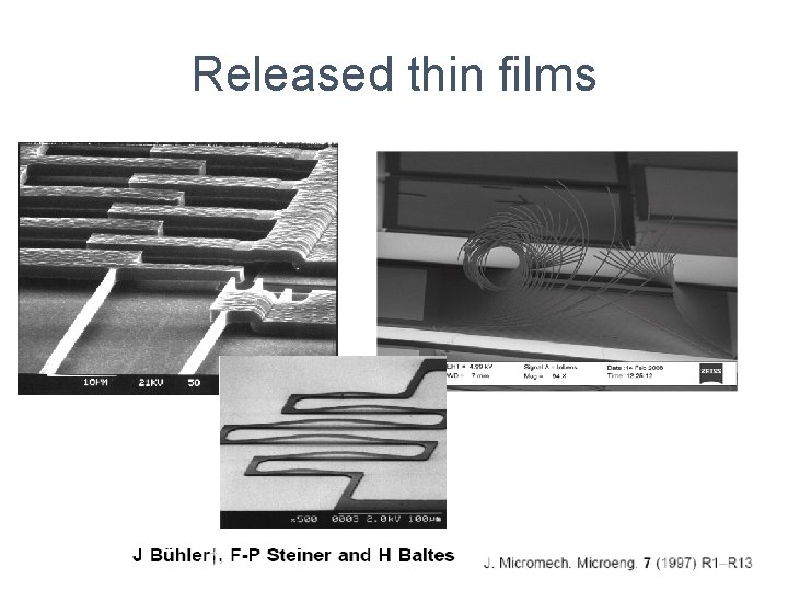
Released thin films

Annealing effects: physical • grain growth (in polycrystalline materials) • crystallization (in amorphous materials) • diffusion of dopants (e. g. boron in silicon) • melting (e. g. aluminum melting point 653 o. C, very low) • thermal expansion and thermal stresses • desorption of adsorbed specie

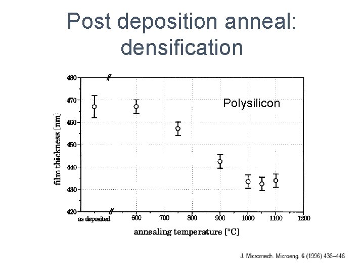
Post deposition anneal: densification Polysilicon

Annealing effects: chemical • reactions at surfaces: -oxidation: 4 Cu + O 2 2 Cu 2 O • reactions between substrate and thin film (Ti. Si 2) beneficial material, low resistivity • reactions between thin films (Al 12 W) harmful material, brittle

More complex films • non-stoichiometric: Ti. N vs. Ti. Nx, x≈0. 8 • hydrogenated: a-Si vs. a-Si: H, 30 at% H • doped: USG vs. PSG, 5 wt% phosphorous metals, oxides: 1 -5% dopant polysilicon: 10 -3. . . 10 -6 dopant • porous (on purpose !) • oriented crystals (piezoelectric, magnetic)

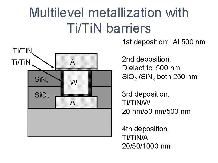
Multilevel metallization with Ti/Ti. N barriers 1 st deposition: Al 500 nm Ti/Ti. N Al Ti/Ti. N Si. Nx Si. O 2 W Al 2 nd deposition: Dielectric: 500 nm Si. O 2 /Si. Nx both 250 nm 3 rd deposition: Ti/Ti. N/W 20 nm/500 nm 4 th deposition: Ti/Ti. N/Al 20/50/1000 nm

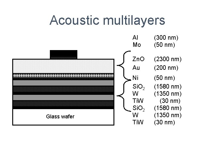
Acoustic multilayers Glass wafer Al Mo (300 nm) (50 nm) Zn. O Au (2300 nm) (200 nm) Ni Si. O 2 W Ti. W (50 nm) (1580 nm) (1350 nm) (30 nm)

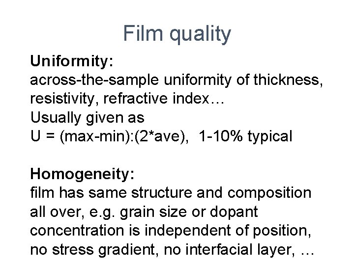
Film quality Uniformity: across-the-sample uniformity of thickness, resistivity, refractive index… Usually given as U = (max-min): (2*ave), 1 -10% typical Homogeneity: film has same structure and composition all over, e. g. grain size or dopant concentration is independent of position, no stress gradient, no interfacial layer, …