Spot 7 Metallization assignments sami franssilaaalto fi Standard
- Slides: 12

Spot 7: Metallization, assignments sami. franssila@aalto. fi

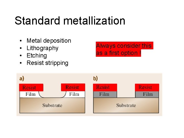
Standard metallization • • Metal deposition Lithography Etching Resist stripping Always consider this as a first option !

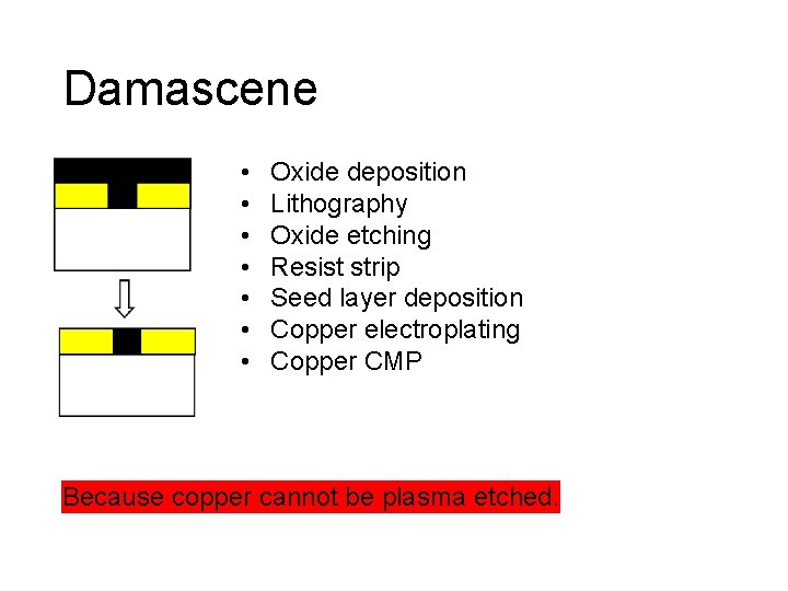
Damascene • • Oxide deposition Lithography Oxide etching Resist strip Seed layer deposition Copper electroplating Copper CMP Because copper cannot be plasma etched.

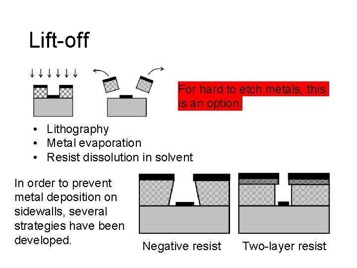
Lift-off For hard to etch metals, this is an option. • Lithography • Metal evaporation • Resist dissolution in solvent In order to prevent metal deposition on sidewalls, several strategies have been developed. Negative resist Two-layer resist

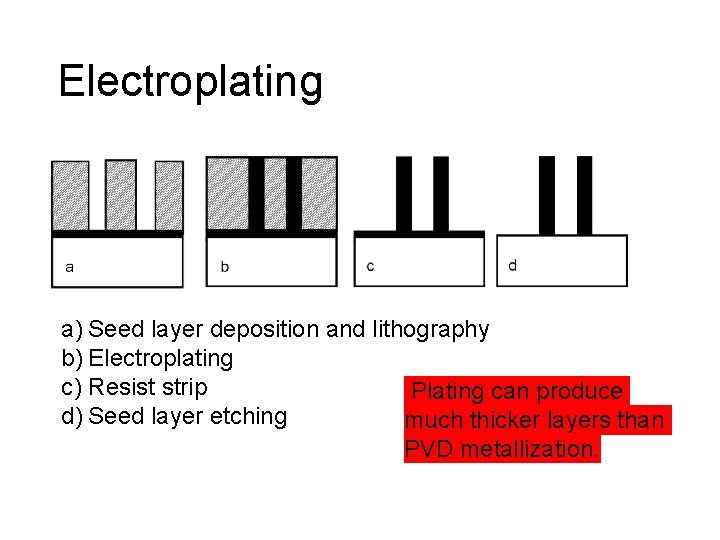
Electroplating a) Seed layer deposition and lithography b) Electroplating c) Resist strip Plating can produce d) Seed layer etching much thicker layers than PVD metallization.

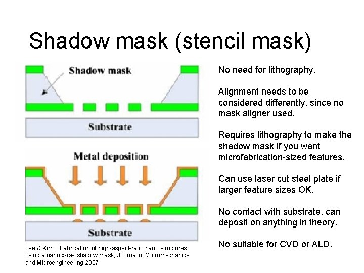
Shadow mask (stencil mask) No need for lithography. Alignment needs to be considered differently, since no mask aligner used. Requires lithography to make the shadow mask if you want microfabrication-sized features. Can use laser cut steel plate if larger feature sizes OK. No contact with substrate, can deposit on anything in theory. Lee & Kim: : Fabrication of high-aspect-ratio nano structures using a nano x-ray shadow mask, Journal of Micromechanics and Microengineering 2007 No suitable for CVD or ALD.

Tasks In all tasks some background info is given, and you job is to choose the right metallization method for the job, and to give arguments for your choice. Also fix missing dimensions. Absolutely no phishing: you choose one way of doing things, and stick to it. “Sputtering (or evaporation)” zero points ! Every group does every assignment.

Task 1: professor Ohm A professor wants to study how Ohm’s law behaves as a function of linewidth. He has an EBL system that is capable of 10 nm minimum resolution. His metallization of choice is Cr/Au.

Task 2: solar copper Solardyne Corp. development engineer wants to replace silver metallization by copper, in order to reduce costs. The metal wires have to carry current of 1 Ampere. Company has contact/proximity 1 X mask aligner.

Task 3: heater Sensor company engineer wants to save costs and to replace platinum heaters with molybdenum heaters in a gas sensor.

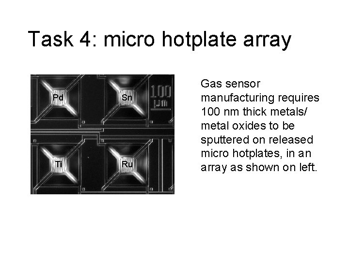
Task 4: micro hotplate array Pd Sn Ti Ru Gas sensor manufacturing requires 100 nm thick metals/ metal oxides to be sputtered on released micro hotplates, in an array as shown on left.

Task 5: 14 nm CMOS Intel engineers want to improve productivity of metallization process in their 14 nm CMOS process. They want to consider metallization options.