
Bulk and SOI MEMS sami franssilaaalto fi Micro
Bulk and SOI MEMS sami. franssila@aalto. fi
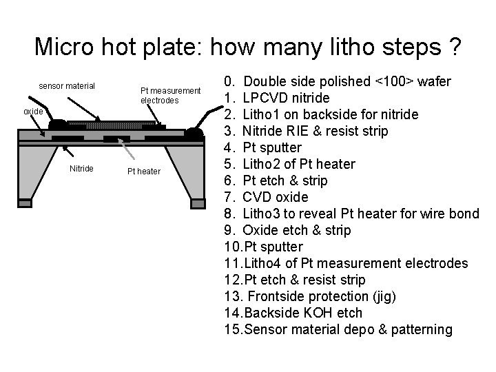
Micro hot plate: how many litho steps ? sensor material Pt measurement electrodes oxide Nitride Pt heater 0. Double side polished <100> wafer 1. LPCVD nitride 2. Litho 1 on backside for nitride 3. Nitride RIE & resist strip 4. Pt sputter 5. Litho 2 of Pt heater 6. Pt etch & strip 7. CVD oxide 8. Litho 3 to reveal Pt heater for wire bond 9. Oxide etch & strip 10. Pt sputter 11. Litho 4 of Pt measurement electrodes 12. Pt etch & resist strip 13. Frontside protection (jig) 14. Backside KOH etch 15. Sensor material depo & patterning
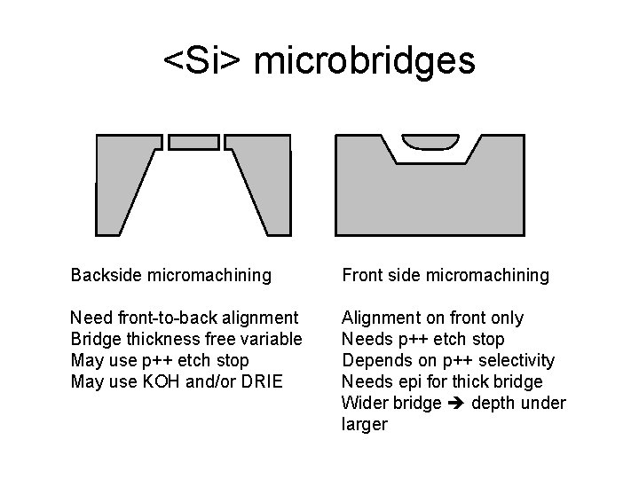
<Si> microbridges Backside micromachining Front side micromachining Need front-to-back alignment Bridge thickness free variable May use p++ etch stop May use KOH and/or DRIE Alignment on front only Needs p++ etch stop Depends on p++ selectivity Needs epi for thick bridge Wider bridge depth under larger
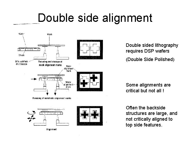
Double side alignment Double sided lithography requires DSP wafers (Double Side Polished) Some alignments are critical but not all ! Often the backside structures are large, and not critically aligned to top side features.
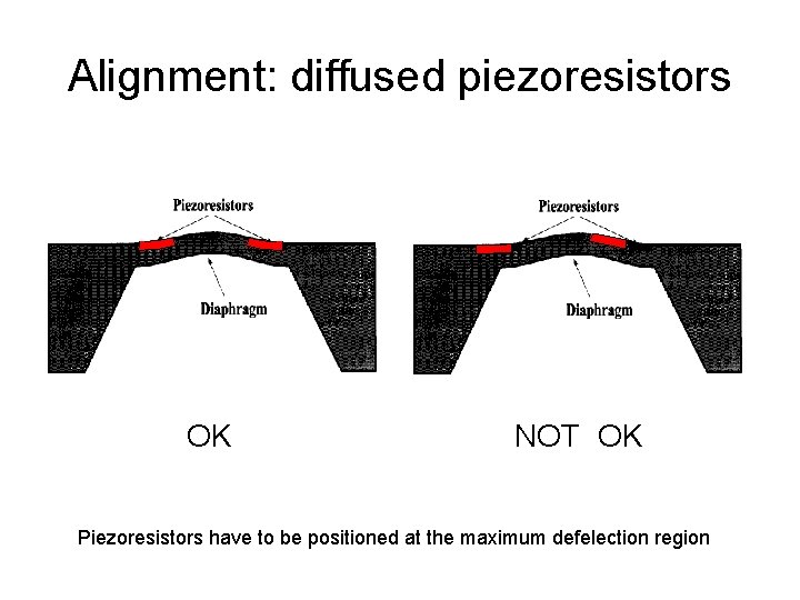
Alignment: diffused piezoresistors OK NOT OK Piezoresistors have to be positioned at the maximum defelection region
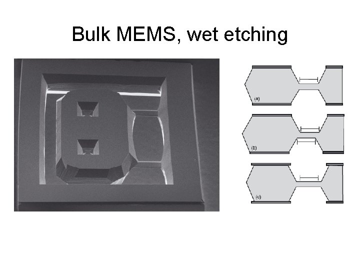
Bulk MEMS, wet etching
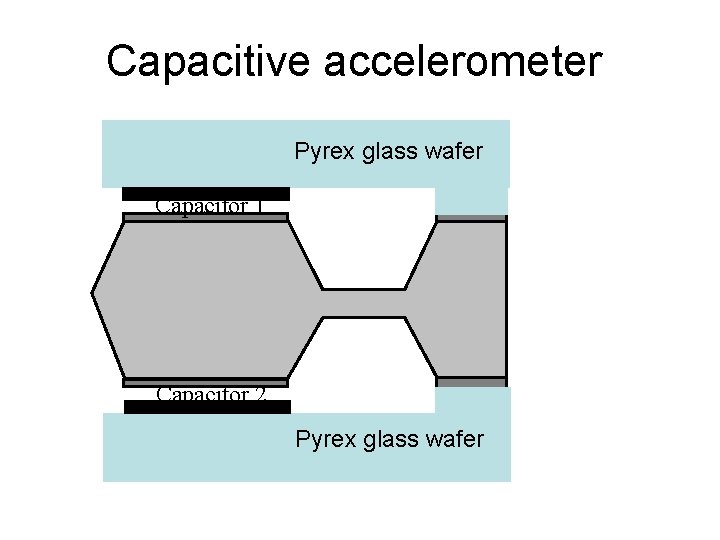
Capacitive accelerometer Pyrex glass wafer Capacitor 1 Capacitor 2 Pyrex glass wafer
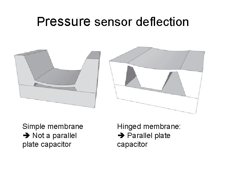
Pressure sensor deflection Simple membrane Not a parallel plate capacitor Hinged membrane: Parallel plate capacitor
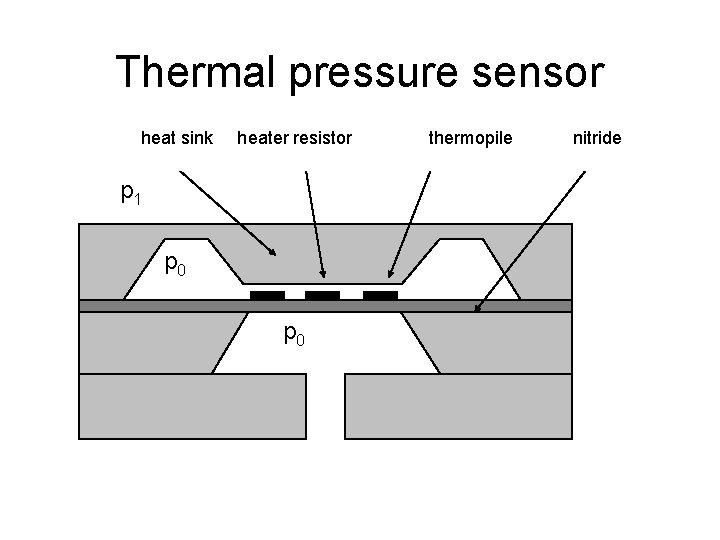
Thermal pressure sensor heat sink heater resistor p 1 p 0 thermopile nitride
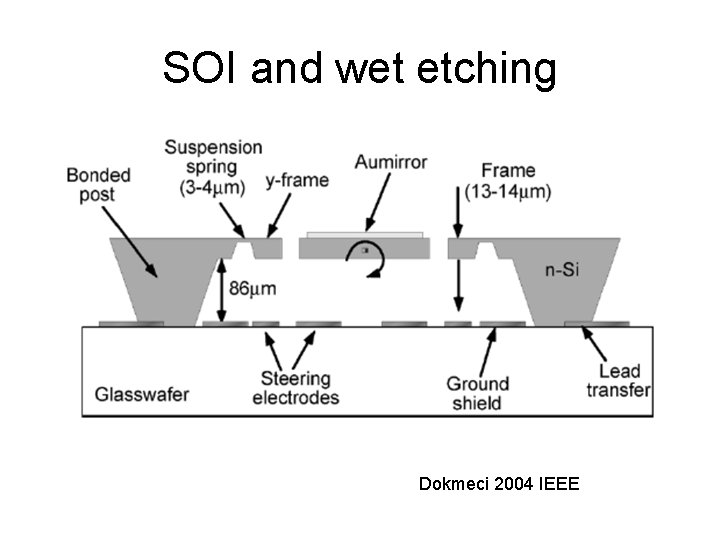
SOI and wet etching Dokmeci 2004 IEEE
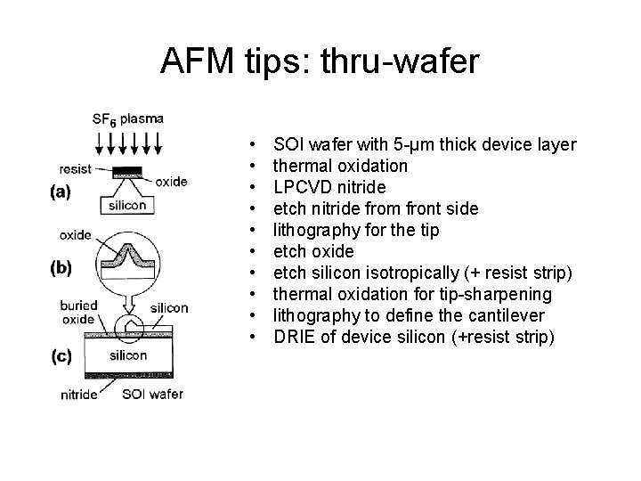
AFM tips: thru-wafer • • • SOI wafer with 5 -μm thick device layer thermal oxidation LPCVD nitride etch nitride from front side lithography for the tip etch oxide etch silicon isotropically (+ resist strip) thermal oxidation for tip-sharpening lithography to define the cantilever DRIE of device silicon (+resist strip)
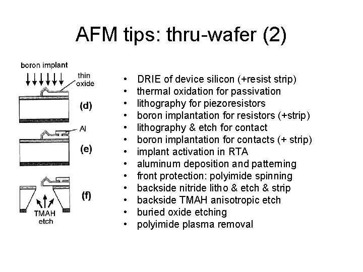
AFM tips: thru-wafer (2) • • • • DRIE of device silicon (+resist strip) thermal oxidation for passivation lithography for piezoresistors boron implantation for resistors (+strip) lithography & etch for contact boron implantation for contacts (+ strip) implant activation in RTA aluminum deposition and patterning front protection: polyimide spinning backside nitride litho & etch & strip backside TMAH anisotropic etch buried oxide etching polyimide plasma removal
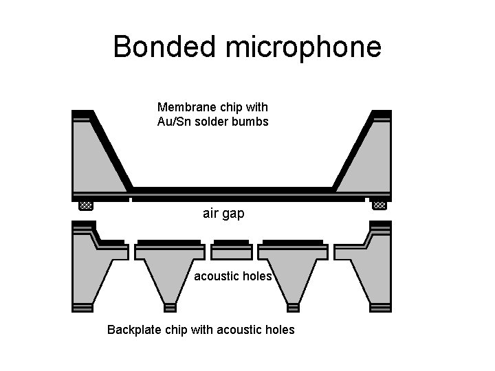
Bonded microphone Membrane chip with Au/Sn solder bumbs air gap acoustic holes Backplate chip with acoustic holes
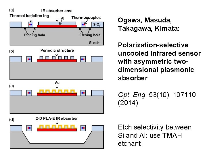
Ogawa, Masuda, Takagawa, Kimata: Polarization-selective uncooled infrared sensor with asymmetric twodimensional plasmonic absorber Opt. Eng. 53(10), 107110 (2014) Etch selectivity between Si and Al: use TMAH etchant
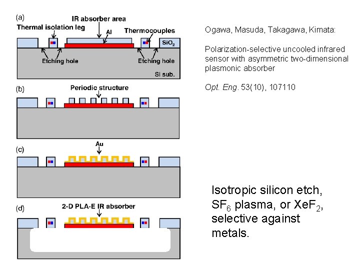
Ogawa, Masuda, Takagawa, Kimata: Polarization-selective uncooled infrared sensor with asymmetric two-dimensional plasmonic absorber Opt. Eng. 53(10), 107110 Isotropic silicon etch, SF 6 plasma, or Xe. F 2, selective against metals.
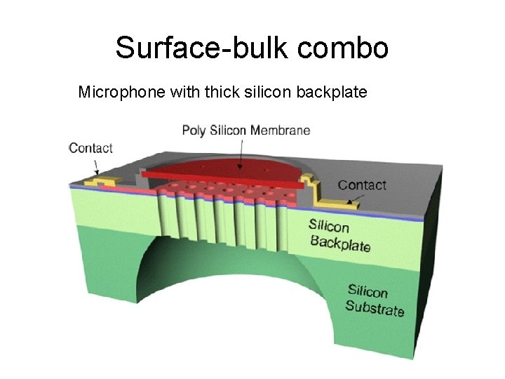
Surface-bulk combo Microphone with thick silicon backplate
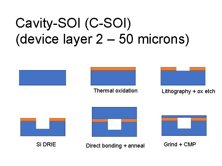
Cavity-SOI (C-SOI) (device layer 2 – 50 microns) Thermal oxidation Si DRIE Direct bonding + anneal Lithography + ox etch Grind + CMP
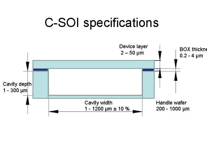
C-SOI specifications Device layer 2 – 50 μm BOX thickne 0. 2 - 4 μm Layer transfer? ? Antti make up something cool. Cavity depth 1 - 300 μm Cavity width 1 - 1200 μm ± 10 % Handle wafer 200 - 1000 μm
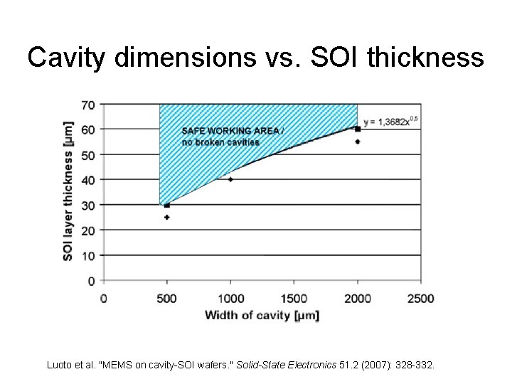
Cavity dimensions vs. SOI thickness Luoto et al. "MEMS on cavity-SOI wafers. " Solid-State Electronics 51. 2 (2007): 328 -332.
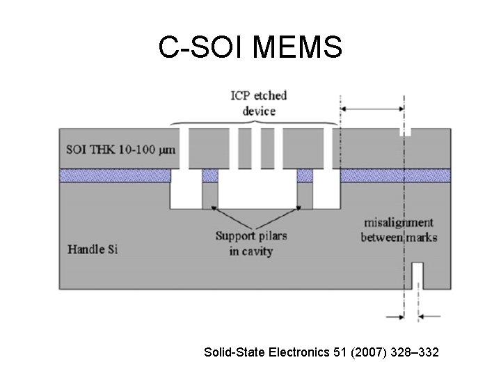
C-SOI MEMS Solid-State Electronics 51 (2007) 328– 332
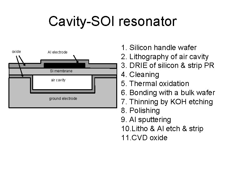
Cavity-SOI resonator oxide Al electrode Si membrane air cavity ground electrode 1. Silicon handle wafer 2. Lithography of air cavity 3. DRIE of silicon & strip PR 4. Cleaning 5. Thermal oxidation 6. Bonding with a bulk wafer 7. Thinning by KOH etching 8. Polishing 9. Al sputtering 10. Litho & Al etch & strip 11. CVD oxide
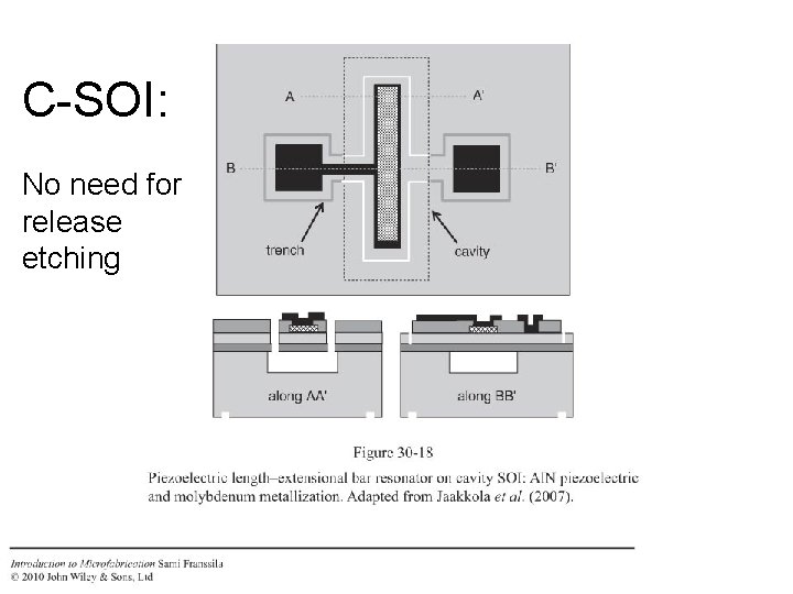
C-SOI: No need for release etching
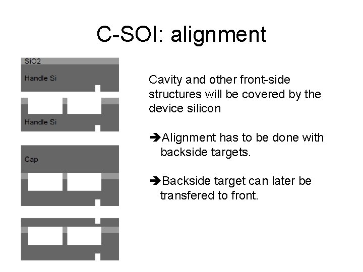
C-SOI: alignment Cavity and other front-side structures will be covered by the device silicon Alignment has to be done with backside targets. Backside target can later be transfered to front.
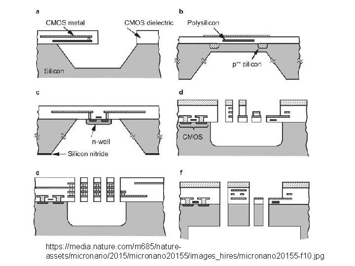
CMOS-MEMS integrated CMOS first MEMS in silicon MEMS in IC thin films MEMS thin films specifically MEMS first plug-up SOI polysilicon thin film MEMS Integrated processes
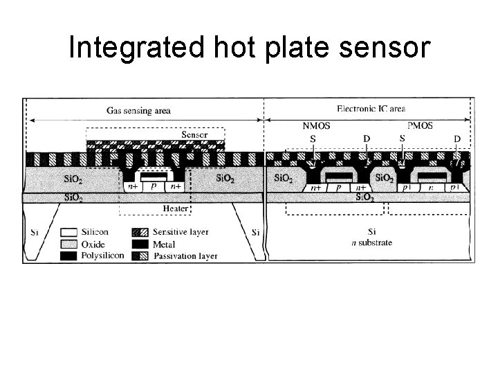
Integrated hot plate sensor
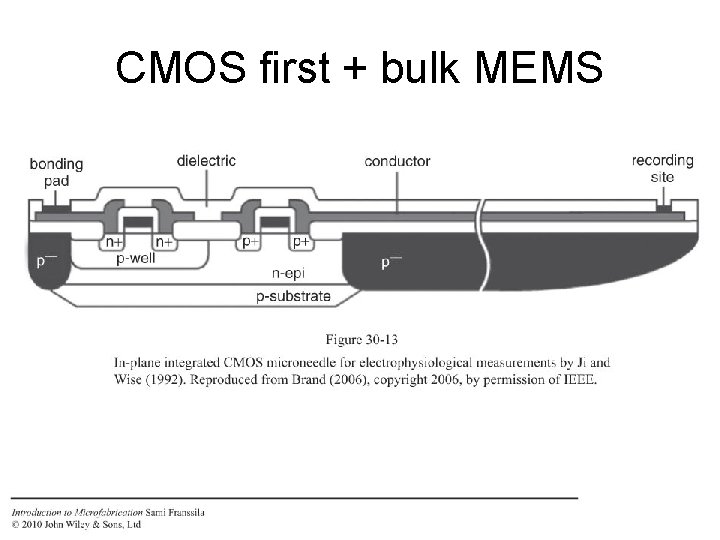
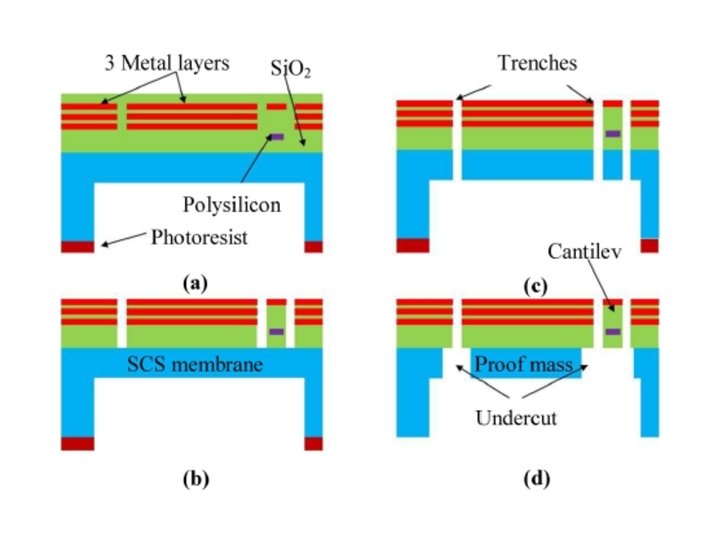
CMOS first + bulk MEMS
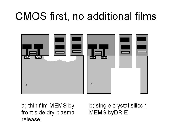
CMOS first, no additional films a a) thin film MEMS by front side dry plasma release; b b) single crystal silicon MEMS by. DRIE
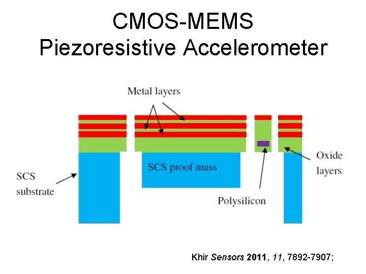
CMOS-MEMS Piezoresistive Accelerometer Khir Sensors 2011, 7892 -7907;
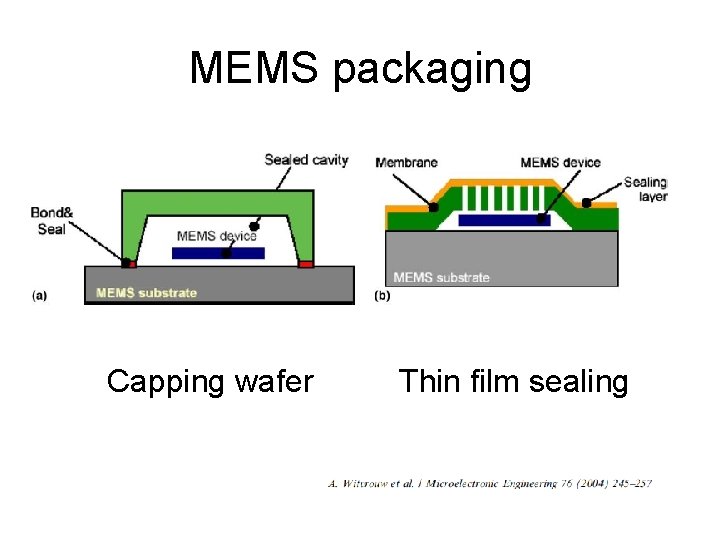
MEMS packaging Capping wafer Thin film sealing
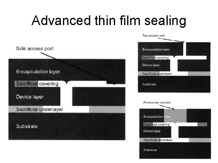
Advanced thin film sealing
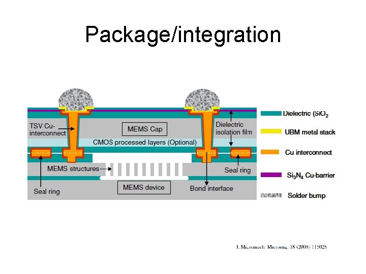
Package/integration
MEMS reliability 1. Solid state devices, no cavities or moving parts. 2. Devices with channels/cavities but no moving parts. 3. Devices with bending/moving but non-contacting parts. 4. Devices with contacting surfaces. 5. Devices with contacting and rubbing surfaces.
MEMS commercialization 1. Solid state devices, no cavities or moving parts. MAJOR INDUSTRY. 2. Devices with channels/cavities but no moving parts. INK JET PRINTERS
3. Devices with bending/oscillating but noncontacting parts. Pressure sensors Accelerometers Microphones IR detectors c. MUTS, p. MUTS Widely available.
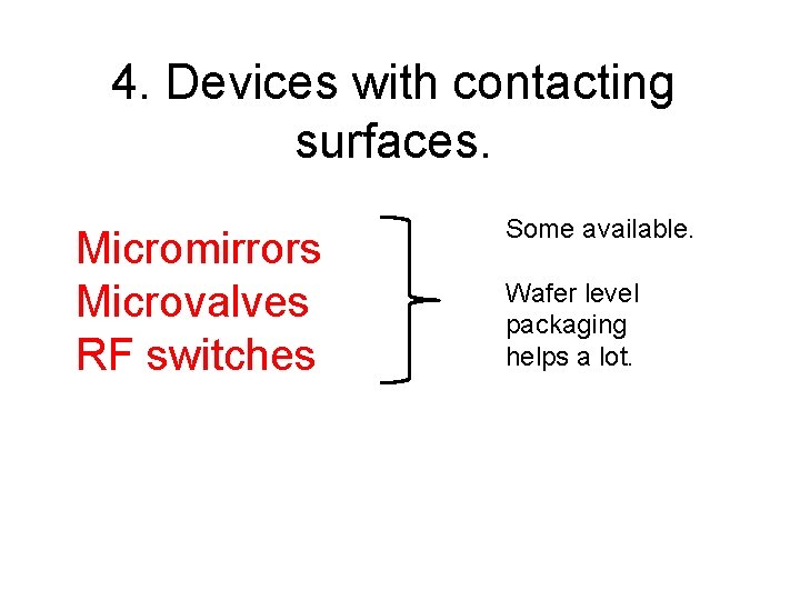
4. Devices with contacting surfaces. Micromirrors Microvalves RF switches Some available. Wafer level packaging helps a lot.
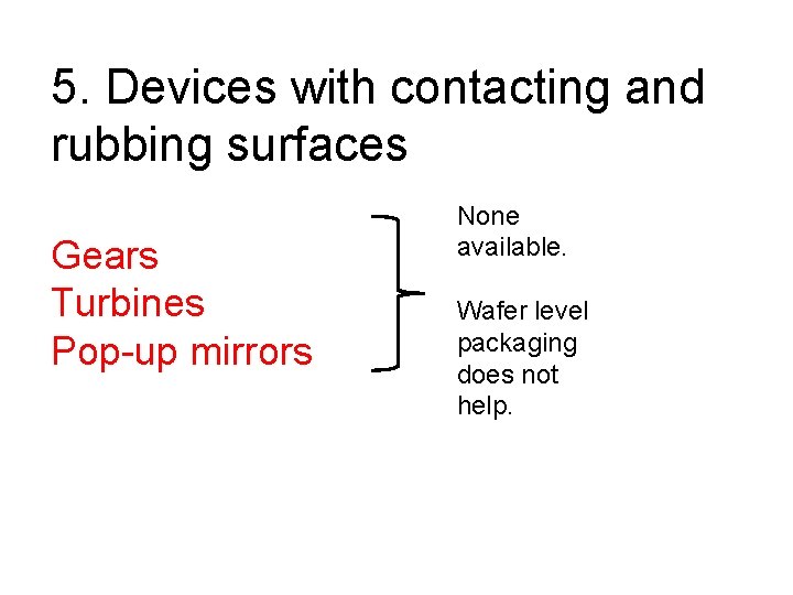
5. Devices with contacting and rubbing surfaces Gears Turbines Pop-up mirrors None available. Wafer level packaging does not help.
https: //media. nature. com/m 685/natureassets/micronano/2015/micronano 20155/images_hires/micronano 20155 -f 10. jpg
- Slides: 39