CVD ALD sami franssilaaalto fi CVD ALD Chemical


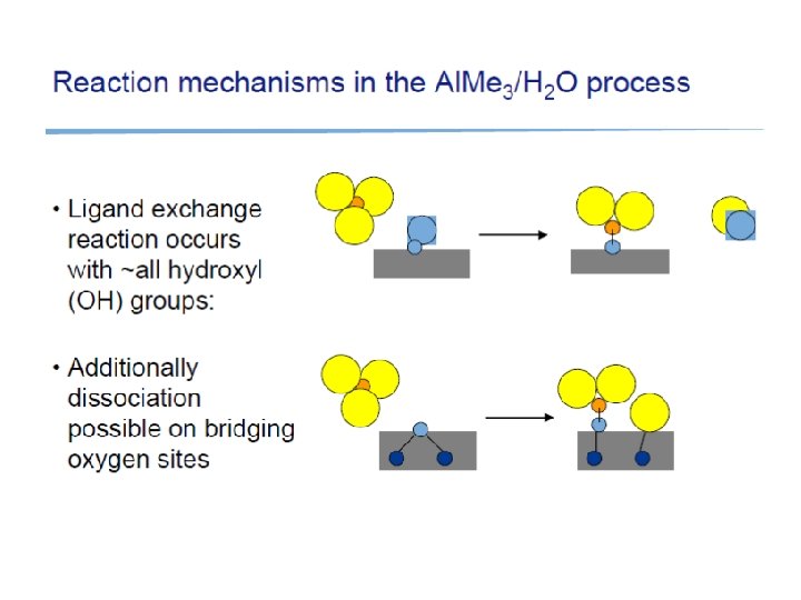
 A batch reactor operating in surface")


")
")

 + 4 NH")
 Polysilicon")


 2 nm thick Ti. N barrier")


")


 Hf. O 2 dielectric marathon test: 2000 wafers")
 ALD Si. O 2 Rate 700 nm/hr Pt")
 Excellent conformality: all surfaces coated by diffusing gaseous")
 Step coverage good also in high aspect ratio grooves, BUT pulse")

 amorphous aluminum oxide Polycrystalline strontium titanate Vehkamäki et al. (2001)")


- Slides: 63
CVD & ALD sami. franssila@aalto. fi
CVD & ALD Chemical Vapor Deposition, CVD Atomic Layer Deposition, ALD Both chemical reactions and fluid dynamics must be considered.
Common CVD reactions
Thermal CVD reactions Gaseous precursor + surface reaction solid film + gaseous byproducts
Thermodynamics of CVD ΔG < 0 for reaction to take place Pierson: Handbook of CVD, p. 22
Silicon CVD from Si. H 4 Unwanted side reaction Wanted deposition reaction Smith: Thin-film deposition
Boundary layer = stagnant gas layer Pierson: Handbook of CVD, p. 36
Boundary layer thickness Re = Reynolds number density viscosity
Surface limited vs. mass transport limited reactions log rate slope = Ea 2 mass transport limited surface reaction limited slope = Ea 1 high T low T (1/T) When temperature is low, surface reaction rate is slow, and overabundance of reactants is available. Reaction is then surface reaction limited. Above a certain temperature all source gas molecules react immediately. The reaction is then in mass-transport limited regime (also known as diffusion limited and supply limited regime).
Si epitaxy: surface controlled vs. mass flow controlled
Surface limited vs. mass transport limited reactions (2) A batch reactor operating in surface reaction limited mode: -slow reaction -many wafers A mass transport limited reactor: -single wafer -high deposition rate
Thermal CVD reactor: gaseous precursors, resistive heating Franssila: Introduction to Microfabrication
Ramped furnace
Thermal CVD reactor: liquid precursors, lamp heating Changsup Ryu, Ph. D thesis, Stanford University, 1998
LRP= Limited Reaction Processing • Very fast and powerful lamp heating • Introduce gases • Flash the lamp T up reaction • Pump away the gases • Introduce new gases • Flash the lamp T up reaction. . .
PECVD: Plasma Enhanced CVD • • Plasma aids in chemical reactions Can be done at low temperatures Wide deposition parameter range High rates (1 -10 nm/s) (thermal 10% of this)
PECVD @ 300 o. C: can be deposited on many materials Oxide: Si. H 4 (g) + N 2 O (g) ==> Si. O 2 + N 2 + 2 H 2 Nitride: 3 Si. H 2 Cl 2 (g) + 4 NH 3 (g) ==> Si 3 N 4 (s) + 6 H 2 (g) + 6 HCl (g)
Si. Nx: H: thermal vs. plasma Thermal CVD at 900 o. C PECVD at 300 o. C Smith: J. Electrochem. Soc. 137 (1990), p. 614
Nitride thermal vs. PECVD (1)
Nitride thermal vs. PECVD (2)
Grain size & roughness Vallat-Sauvain
Hydrogen in PECVD films 3 Si. H 2 Cl 2 (g) + 4 NH 3 (g) ==> Si 3 N 4 (s) + 6 H 2 (g) + 6 HCl (g) 30 at% hydrogen is usual; 3 -5% is as small as it gets
CVD films lose thickness upon anneal (H 2 escapes) Polysilicon
Film quality: etch rate Low pressure equals more bombardment, and thus denser film, and compressive stress With Si. O 2, BHF etch rate is a film quality measure (should be no more than 2 X thermal oxide reference Hey et al: Solid State Technology April 1990, p. 139
Stress affects by: pressure frequency temperature
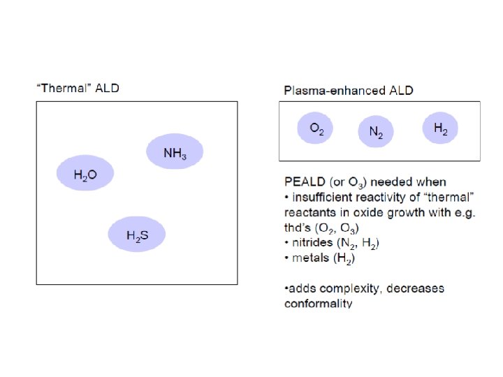
ALD: Atomic Layer Deposition Precursors introduced in pulses, with purging in-between
Materials deposited by ALD Important missing materials: • silicon nitride
ALD applications 1 nm thick catalysts (Pt, Pd) 2 nm thick Ti. N barrier layers underneath copper 6 nm thick CMOS gate oxides like Hf. O 2 10 nm thick etch masks for plasma etching (Al 2 O 3) 30 nm thick antireflection coatings in solar cells (Al 2 O 3) 200 nm thick barrier layers in flat panel displays (Al 2 O 3)
ALD applications
ALD process based on: conformal film
Surface saturation Irreversible saturation ALD reactions: Surface saturates with a monolayer of precursor, strong chemisorption (=chemical bonds formed) Reversible saturation: Physisorption only (weak bonds like van der Waals): once precursor flux is stopped, surface specie will desorb. Irreversible nonsaturating. CVD regime: more reactants in, more film is deposited (continuosly)
ALD window
Pulse-by-pulse mass monitoring
Growth rate
Layer thickness control
Layer thickness (2)
Layer thickness: nanolaminates Al 2 O 3 and Ta 2 O 5 Adriana Szeghalmi, Stephan Senz, Mario Bretschneider, Ulrich Gösele, and Mato Knez, APL 2009
Impurities in ALD
ALD uniformity (=thickness across the wafer) Hf. O 2 dielectric marathon test: 2000 wafers
Uniformity (2) ALD Si. O 2 Rate 700 nm/hr Pt
ALD conformality (=step coverage in microstructures) Excellent conformality: all surfaces coated by diffusing gaseous precursors in the surface reaction limited mode. Al 2 O 3/Ti. O 2 nanolaminate Ti. N barrier
Step coverage (2) Step coverage good also in high aspect ratio grooves, BUT pulse lenghts have to to be increased (in coating porous materials, pulses last for minutes !!).
Structure: amorphous vs. polycrystalline ?
Structure (2) amorphous aluminum oxide Polycrystalline strontium titanate Vehkamäki et al. (2001)
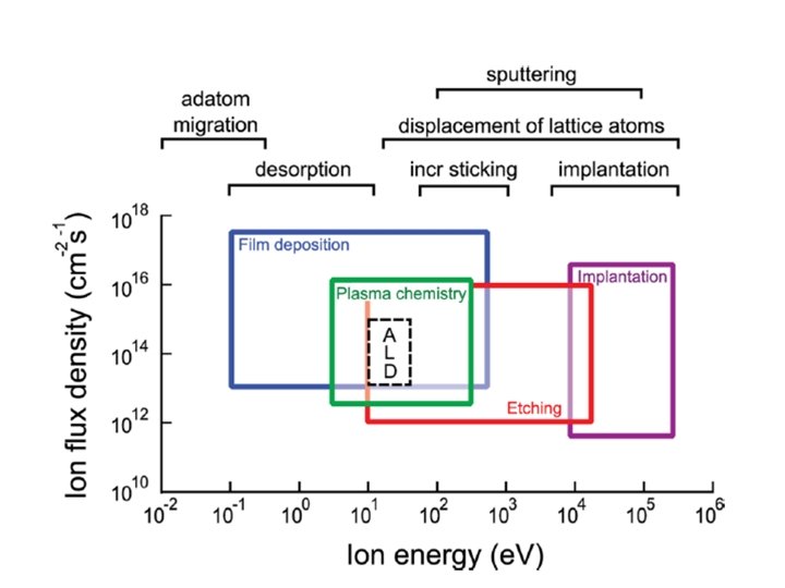
Plasma-enhanced ALD
PEALD
Plasma ALD benefits Plasma can break down precursors at lower temperature New precursors become available because plasma can break down precursors that could not be used in thermal ALD Ions can kick of loosely bound specie from surface, densifying the film
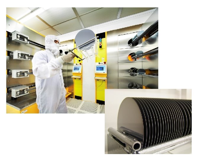
ALD reactors: single wafer
ALD reactors: batch
Gas pulsing
Spatial ALD jes. ecsdl. org
Spatial ALD reactors www. blog. baldengineering. com/2014_
Spatial ALD since 1977 !
ALD process development
PVD CVD & ALD Atoms as source material Molecules as source materials Solid source materials Solid, liquid, gas precursors Vacuum/high vacuum Fluid dynamics important Elemental films mostly Molecular/compound films mostly, Chemical bonds broken & formed Room temperature Alloy films easily (W: N) Needs elevated temperatures (or plasma activation) Elements and compounds OK, alloys more difficult One process, many materials Each process materials specific Al, Au, Cu, Pt, … Si. O 2, Si 3 N 4, Al 2 O 3, Hf. O 2, … Si, W
ALD CVD
CVD vs. ALD difference
Summary • Thermal CVD: excellent film quality • PECVD: reasonable film quality at low T • ALD: excellent film quality at low T • Thermal CVD: high temperature needed • PECVD: very high rate possible • ALD: best for very thin films