Electrical and optical properties of thin films sami

- Slides: 47

Electrical and optical properties of thin films sami. franssila@aalto. fi

Outline • • Metallic (conductive) films Contact resistance Low dielectric constant films High dielectric constant films Optics in thin films Metallic mirrors Dielectric mirrors Other optical components

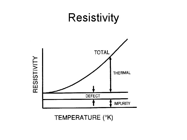
Resistivity

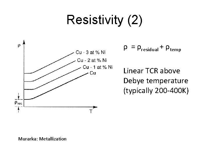
Resistivity (2) ρ = ρresidual + ρtemp Linear TCR above Debye temperature (typically 200 -400 K) Murarka: Metallization

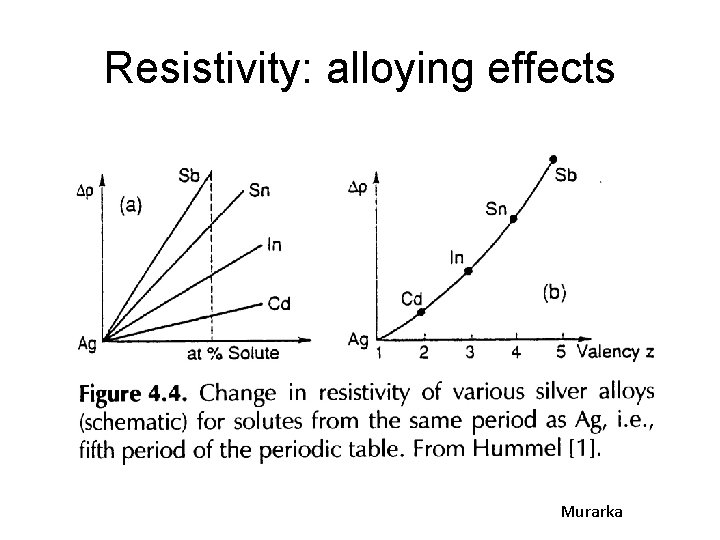
Resistivity: alloying effects Murarka

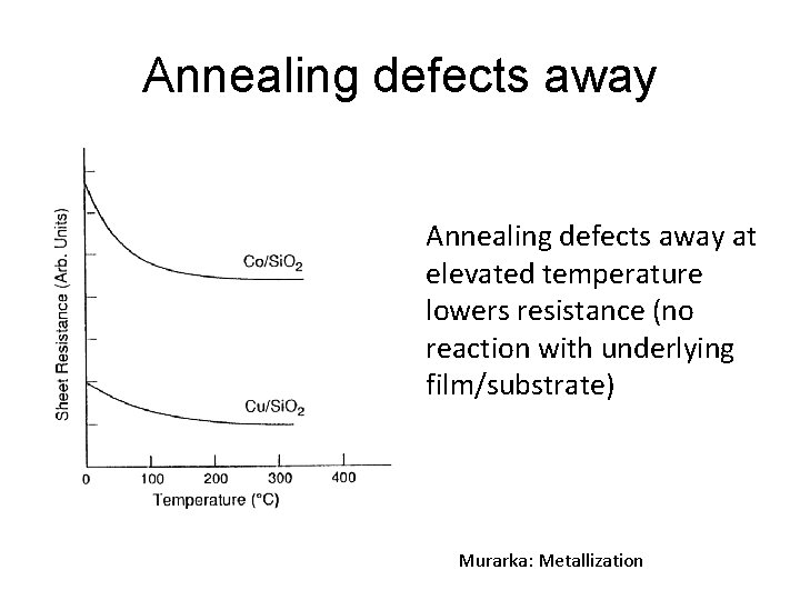
Annealing defects away at elevated temperature lowers resistance (no reaction with underlying film/substrate) Murarka: Metallization

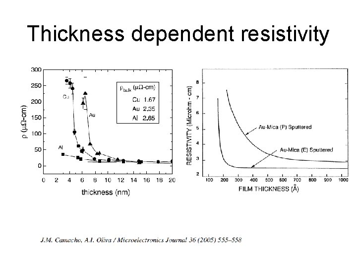
Thickness dependent resistivity

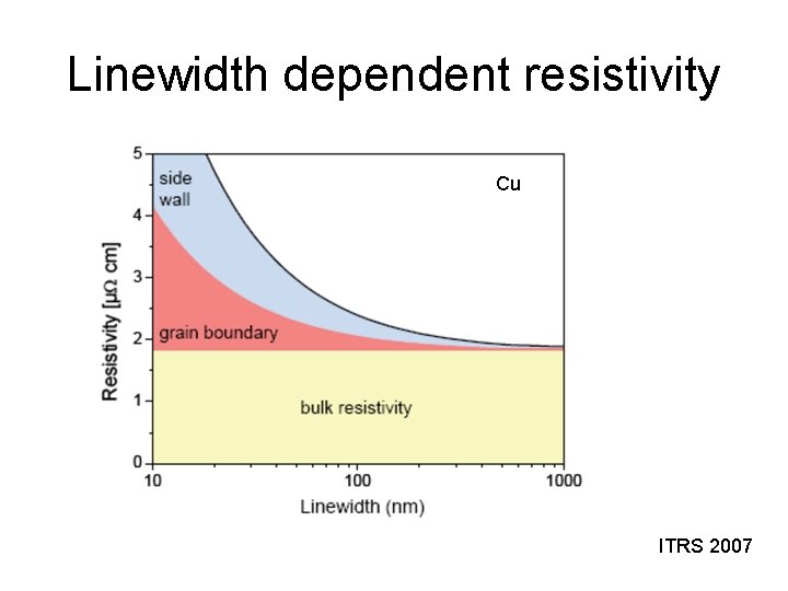
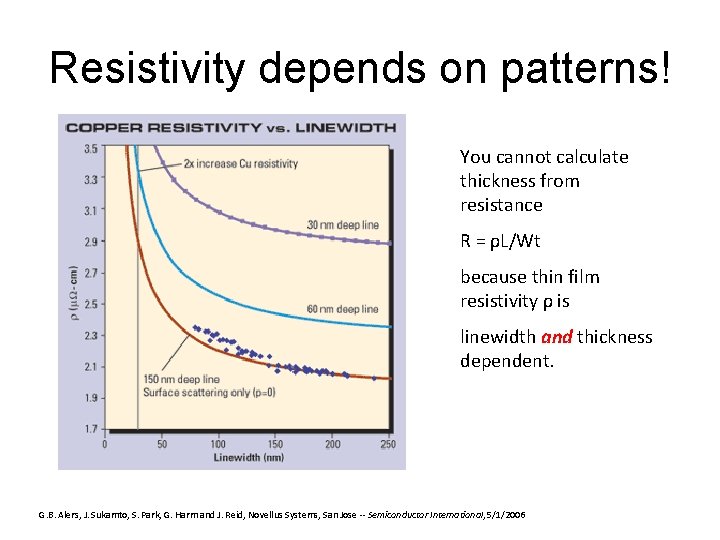
Linewidth dependent resistivity Cu ITRS 2007

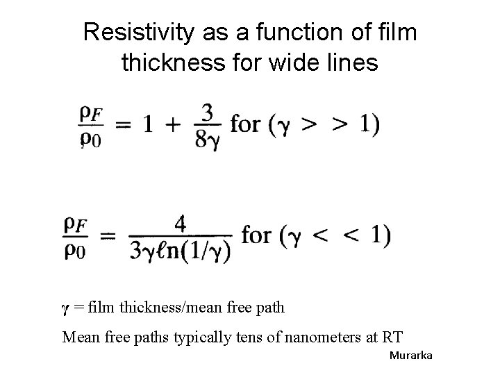
Resistivity as a function of film thickness for wide lines γ = film thickness/mean free path Mean free paths typically tens of nanometers at RT Murarka

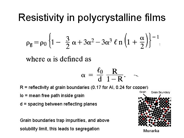
Resistivity in polycrystalline films R = reflectivity at grain boundaries (0. 17 for Al, 0. 24 for copper) lo = mean free path inside grain d = spacing between reflecting planes Grain boundaries trap impurities, and above solubility limit, this leads to segregation Murarka

Resistivity depends on patterns! You cannot calculate thickness from resistance R = ρL/Wt because thin film resistivity ρ is linewidth and thickness dependent. G. B. Alers, J. Sukamto, S. Park, G. Harm and J. Reid, Novellus Systems, San Jose -- Semiconductor International, 5/1/2006

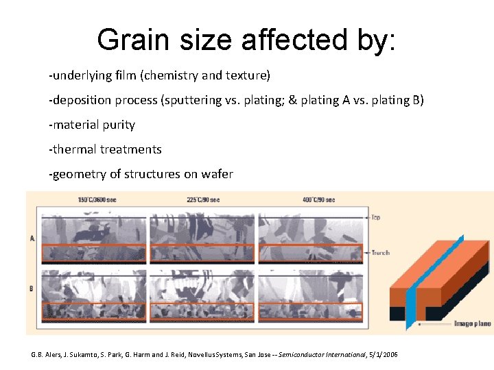
Grain size affected by: -underlying film (chemistry and texture) -deposition process (sputtering vs. plating; & plating A vs. plating B) -material purity -thermal treatments -geometry of structures on wafer G. B. Alers, J. Sukamto, S. Park, G. Harm and J. Reid, Novellus Systems, San Jose -- Semiconductor International, 5/1/2006

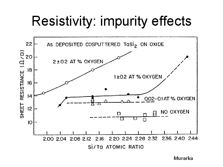
Resistivity: impurity effects Murarka

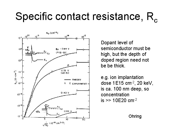
Specific contact resistance, Rc Dopant level of semiconductor must be high, but the depth of doped region need not be be thick. e. g. ion implantation dose 1 E 15 cm-2, 20 ke. V, is ca. 100 nm deep, so concentration is >> 10 E 20 cm-2 Ohring

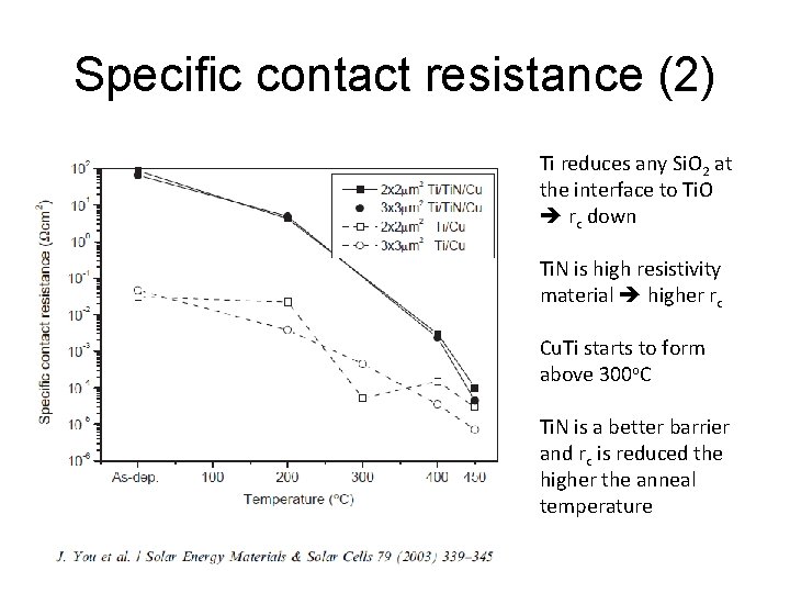
Specific contact resistance (2) Ti reduces any Si. O 2 at the interface to Ti. O rc down Ti. N is high resistivity material higher rc Cu. Ti starts to form above 300 o. C Ti. N is a better barrier and rc is reduced the higher the anneal temperature

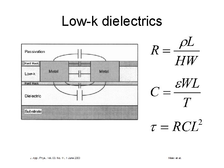
Low-k dielectrics

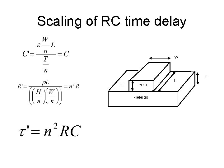
Scaling of RC time delay W T H metal dielectric L

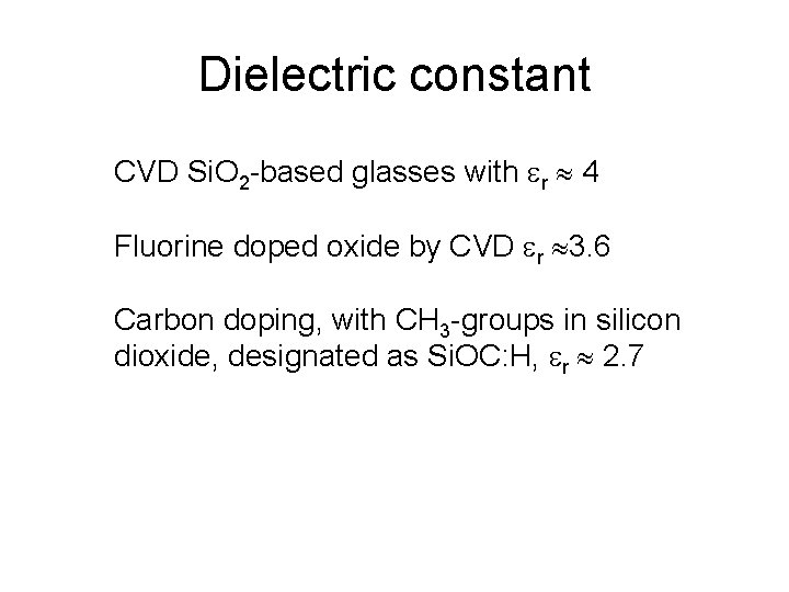
Dielectric constant CVD Si. O 2 -based glasses with r 4 Fluorine doped oxide by CVD r 3. 6 Carbon doping, with CH 3 -groups in silicon dioxide, designated as Si. OC: H, r 2. 7

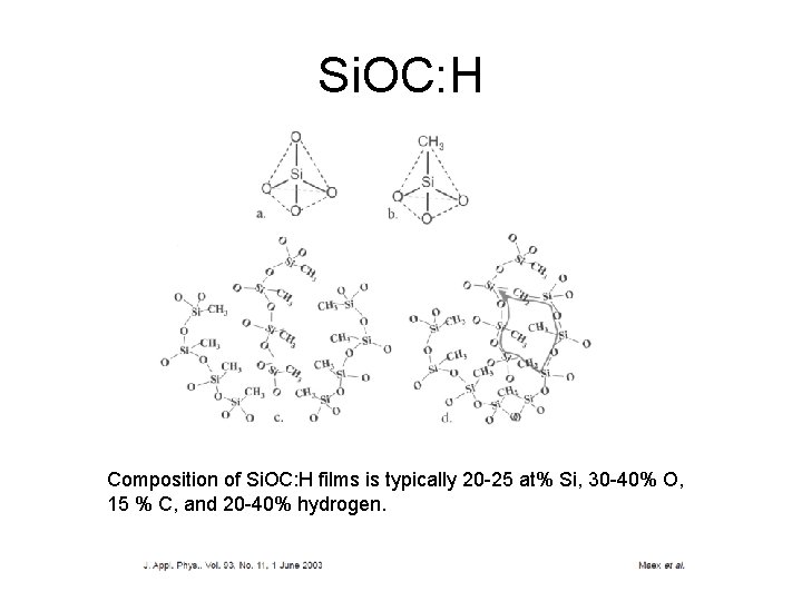
Si. OC: H Composition of Si. OC: H films is typically 20 -25 at% Si, 30 -40% O, 15 % C, and 20 -40% hydrogen.

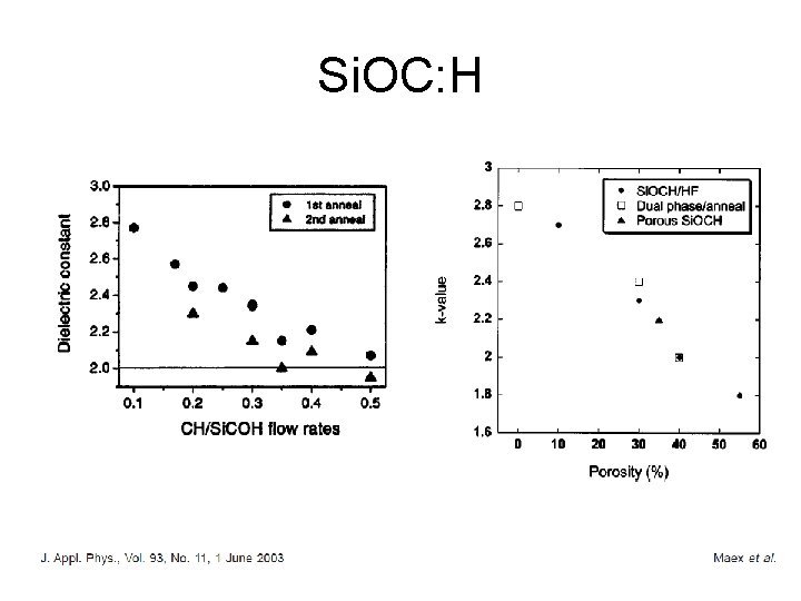
Si. OC: H

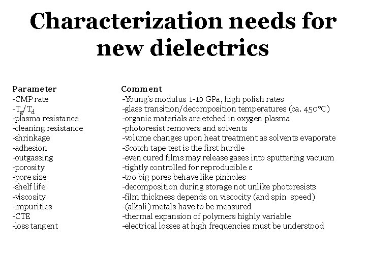
Characterization needs for new dielectrics Parameter -CMP rate -Tg/Td -plasma resistance -cleaning resistance -shrinkage -adhesion -outgassing -porosity -pore size -shelf life -viscosity -impurities -CTE -loss tangent Comment -Young’s modulus 1 -10 GPa, high polish rates -glass transition/decomposition temperatures (ca. 450 C) -organic materials are etched in oxygen plasma -photoresist removers and solvents -volume changes upon heat treatment as solvents evaporate -Scotch tape test is the first hurdle -even cured films may release gases into sputtering vacuum -tightly controlled for reproducible -too big pores behave like pinholes -decomposition during storage not unlike photoresists -film thickness depends on viscocity (and spin speed) -(alkali) metals have to be measured -thermal expansion of polymers highly variable -electrical losses at high frequencies must be understood

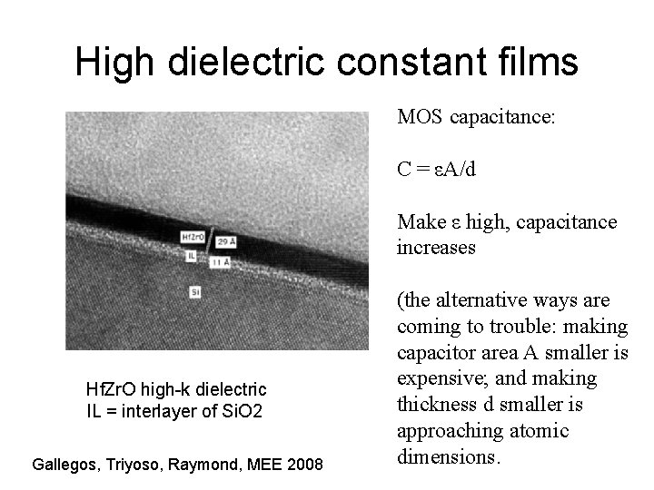
High dielectric constant films MOS capacitance: C = εA/d Make ε high, capacitance increases Hf. Zr. O high-k dielectric IL = interlayer of Si. O 2 Gallegos, Triyoso, Raymond, MEE 2008 (the alternative ways are coming to trouble: making capacitor area A smaller is expensive; and making thickness d smaller is approaching atomic dimensions.

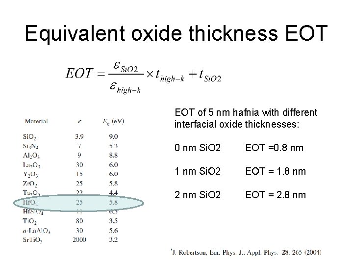
Equivalent oxide thickness EOT of 5 nm hafnia with different interfacial oxide thicknesses: 0 nm Si. O 2 EOT =0. 8 nm 1 nm Si. O 2 EOT = 1. 8 nm 2 nm Si. O 2 EOT = 2. 8 nm

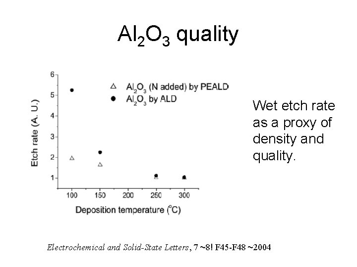
Al 2 O 3 quality Wet etch rate as a proxy of density and quality. Electrochemical and Solid-State Letters, 7 ~8! F 45 -F 48 ~2004

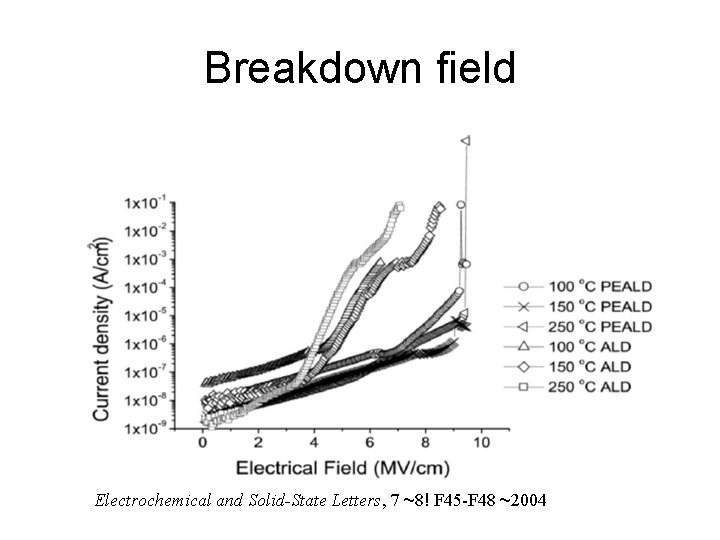
Breakdown field Electrochemical and Solid-State Letters, 7 ~8! F 45 -F 48 ~2004

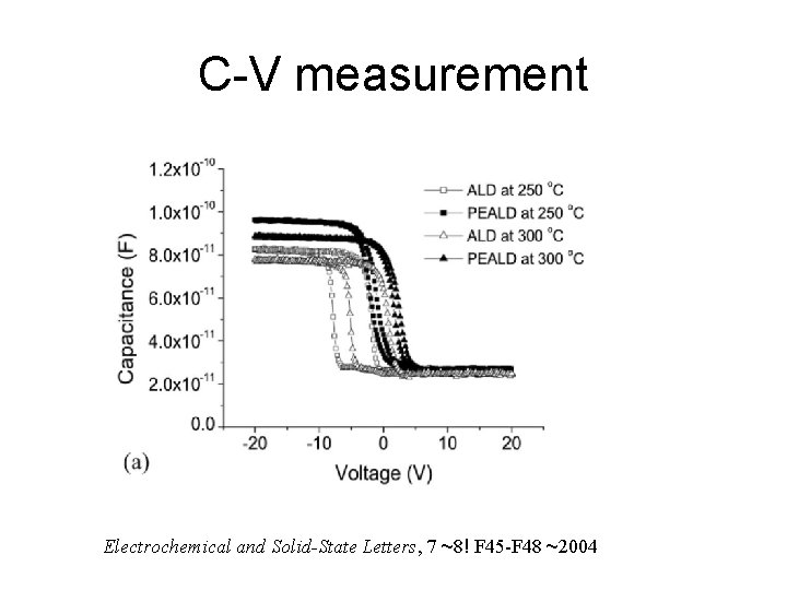
C-V measurement Electrochemical and Solid-State Letters, 7 ~8! F 45 -F 48 ~2004

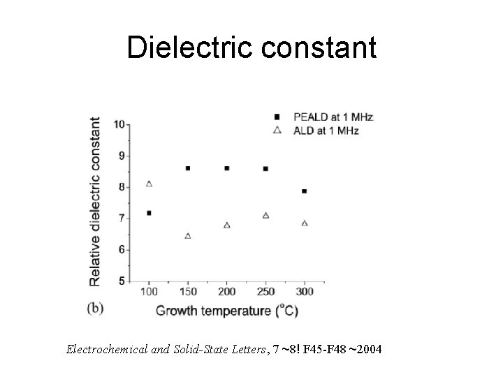
Dielectric constant Electrochemical and Solid-State Letters, 7 ~8! F 45 -F 48 ~2004

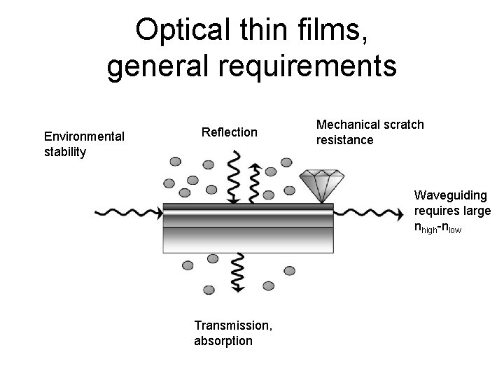
Optical thin films, general requirements Environmental stability Reflection Mechanical scratch resistance Waveguiding requires large nhigh-nlow Transmission, absorption

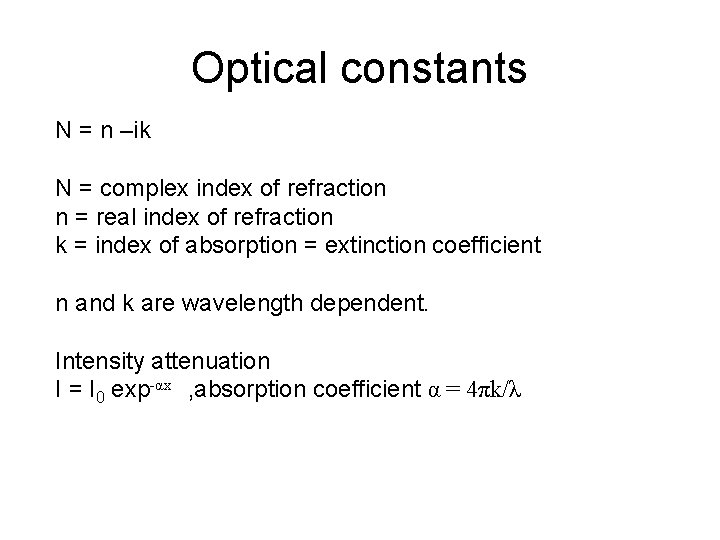
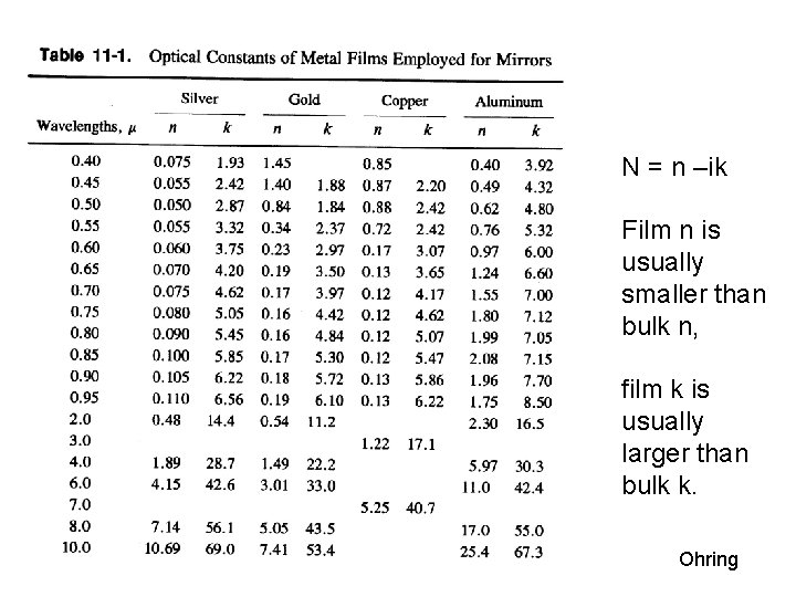
Optical constants N = n –ik N = complex index of refraction n = real index of refraction k = index of absorption = extinction coefficient n and k are wavelength dependent. Intensity attenuation I = I 0 exp-αx , absorption coefficient α = 4πk/λ

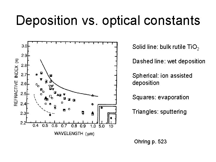
Deposition vs. optical constants Solid line: bulk rutile Ti. O 2 Dashed line: wet deposition Spherical: ion assisted deposition Squares: evaporation Triangles: sputtering Ohring p. 523

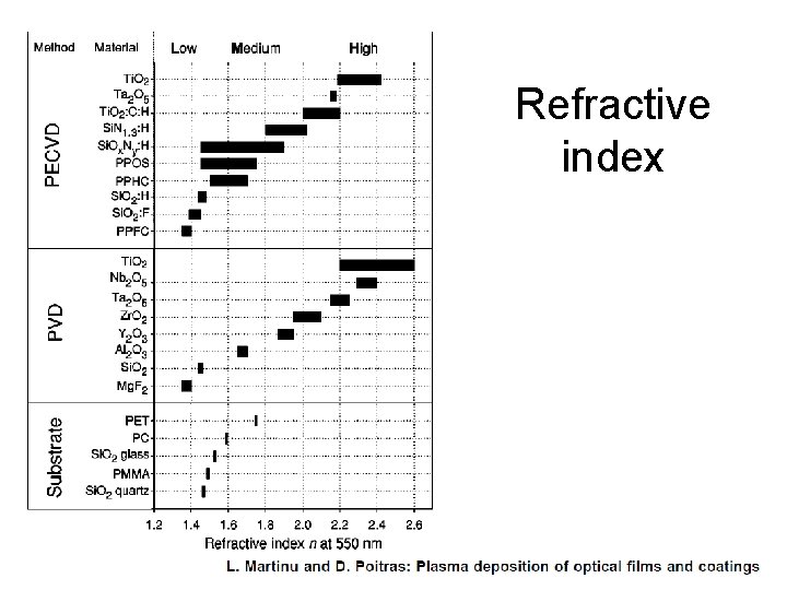
Refractive index

N = n –ik Film n is usually smaller than bulk n, film k is usually larger than bulk k. Ohring

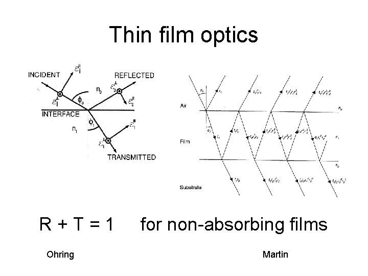
Thin film optics R+T=1 Ohring for non-absorbing films Martin

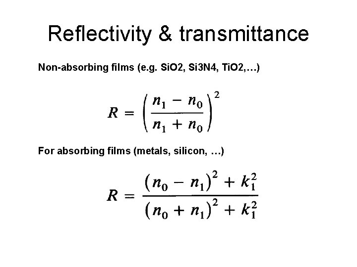
Reflectivity & transmittance Non-absorbing films (e. g. Si. O 2, Si 3 N 4, Ti. O 2, …) For absorbing films (metals, silicon, …)

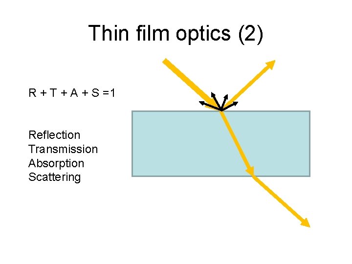
Thin film optics (2) R + T + A + S =1 Reflection Transmission Absorption Scattering

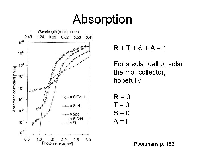
Absorption R+T+S+A=1 For a solar cell or solar thermal collector, hopefully R=0 T=0 S=0 A =1 Poortmans p. 182

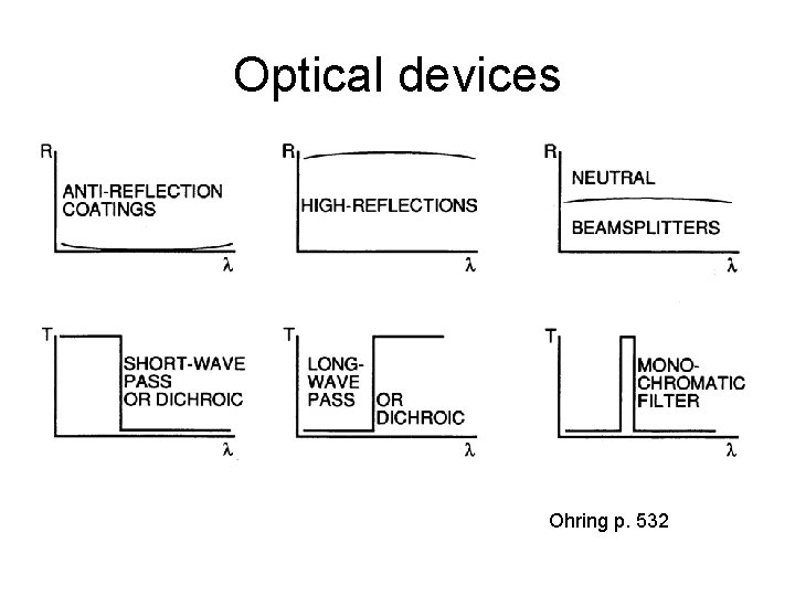
Optical devices Ohring p. 532

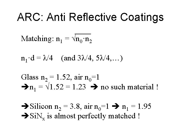
ARC: Anti Reflective Coatings Matching: n 1 = √n 0·n 2 n 1·d = λ/4 (and 3λ/4, 5λ/4, …) Glass n 2 = 1. 52, air n 0=1 n 1 = √ 1. 52 = 1. 23 no such material ! Silicon n 2 = 3. 8, air n 0=1 n 1 = 1. 95 Si. Nx is almost perfectly matched !

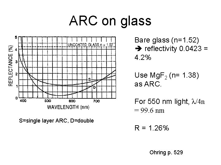
ARC on glass Bare glass (n=1. 52) reflectivity 0. 0423 = 4. 2% Use Mg. F 2 (n= 1. 38) as ARC. For 550 nm light, λ/4 n = 99. 6 nm S=single layer ARC, D=double R = 1. 26% Ohring p. 529

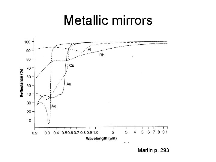
Metallic mirrors Ohring p. 512 Martin p. 293

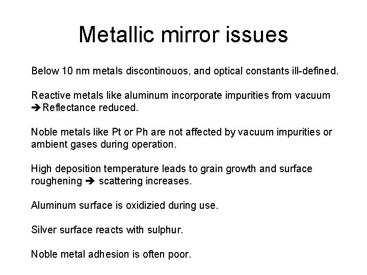
Metallic mirror issues Below 10 nm metals discontinouos, and optical constants ill-defined. Reactive metals like aluminum incorporate impurities from vacuum Reflectance reduced. Noble metals like Pt or Ph are not affected by vacuum impurities or ambient gases during operation. High deposition temperature leads to grain growth and surface roughening scattering increases. Aluminum surface is oxidizied during use. Silver surface reacts with sulphur. Noble metal adhesion is often poor.

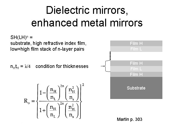
Dielectric mirrors, enhanced metal mirrors SH(LH)n = substrate, high refractive index film, low+high film stack of n-layer pairs n. Ht. H = λ/4 condition for thicknesses Film H Film L Film H Substrate Martin p. 303

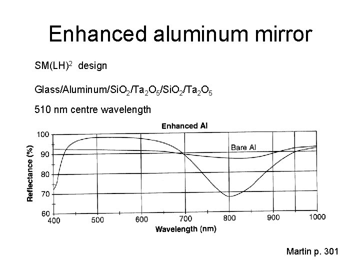
Enhanced aluminum mirror SM(LH)2 design Glass/Aluminum/Si. O 2/Ta 2 O 5 510 nm centre wavelength Martin p. 301

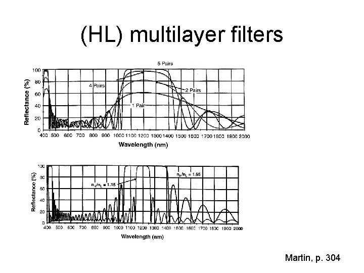
(HL) multilayer filters Martin, p. 304

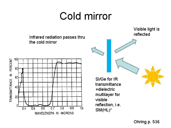
Cold mirror Visible light is reflected Infrared radiation passes thru the cold mirror Si/Ge for IR transmittance +dielectric multilayer for visible reflection, i. e. SM(HL)n Ohring p. 536

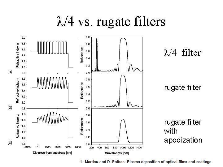
λ/4 vs. rugate filters λ/4 filter rugate filter with apodization

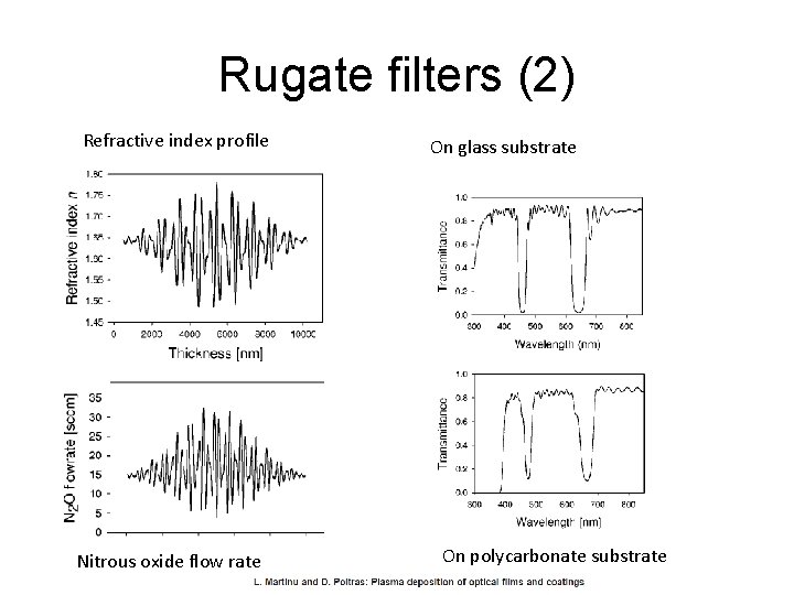
Rugate filters (2) Refractive index profile Nitrous oxide flow rate On glass substrate On polycarbonate substrate