Thin films are thin material layers ranging from
- Slides: 22

Thin films are thin material layers ranging from fractions of a nanometre to several micrometres in thickness. • Ferromagnetic thin films are used as computer memory. • The relatively high hardness and inertness of ceramic materials make thin coating for protection of substrate materials against corrosion, oxidation and wear. • The use of such coatings on cutting tools can extend the life of these items by several orders of magnitude. Thin-film deposition is a technique for depositing a thin film of material onto a substrate or onto previously deposited layers. "Thin" is a relative term, but most deposition techniques allow layer thickness to be controlled within a few tens of nanometers, and some allow single layers of atoms to be deposited at a time (molecular beam epitaxy). 1

Chemical deposition is further categorized by the phase of the precursor: 1. Plating relies on liquid precursors, often a solution of water with a salt of the metal to be deposited. The most commercially important process is electroplating. 2. Chemical Solution Deposition (CSD) uses a liquid precursor, usually a solution of organometallic powders dissolved in an organic solvent. 3. Chemical vapor deposition (CVD) generally uses a gasphase precursor, often a halide or hydride of the element to be deposited. 4. In the case of MOCVD, an organometallic gas is used. Commercial techniques often use very low pressures of precursor gas. 2

Deposition techniques fall into two broad categories, chemical or physical. Chemical deposition: A fluid precursor undergoes a chemical change at a solid surface, leaving a solid layer. Example: formation of soot on a cool object when it is placed inside a flame. Since the fluid surrounds the solid object, deposition happens on every surface, with little regard to direction. 3

• Physical vapor deposition (PVD) is a variety of vacuum deposition and is a general term used to describe any of a variety of methods to deposit thin films by the condensation of a vaporized form of the material onto various surfaces (e. g. , onto semiconductor wafers). • The coating method involves purely physical processes such as high temperature vacuum evaporation or plasma sputter bombardment rather than involving a chemical reaction at the surface to be coated as in chemical vapor deposition. • Physical deposition uses mechanical or thermodynamic means to produce a thin film of solid. Example is the formation of frost. Since most engineering materials are held together by relatively high energies, and chemical reactions are not used to store these energies, commercial physical deposition systems tend to require a low-pressure vapor environment to function properly; most can be classified as Physical vapor deposition or PVD. • The material to be deposited is placed in an energetic, entropic environment, so that particles of material escape its surface. Facing this source is a cooler surface which draws energy from these particles as they arrive, allowing them to form a solid layer. The whole system is kept in a vacuum deposition chamber, to allow the particles to travel as freely as possible. Since particles tend to follow a straight path, films deposited by physical means are commonly directional. 4

Types of PVD : • Evaporative deposition: In which the material to be deposited is heated to a high vapor pressure by electrically resistive heating in "low" vacuum. • Electron beam physical vapor deposition: In which the material to be deposited is heated to a high vapor pressure by electron bombardment in "high" vacuum. • Sputter deposition: In which a glow plasma discharge (usually localized around the "target" by a magnet) bombards the material sputtering some away as a vapor. • Cathodic Arc Deposition: In which a high power arc directed at the target material blasts away some into a vapor. • Pulsed laser deposition: In which a high power laser ablates material from the target into a vapor. 5

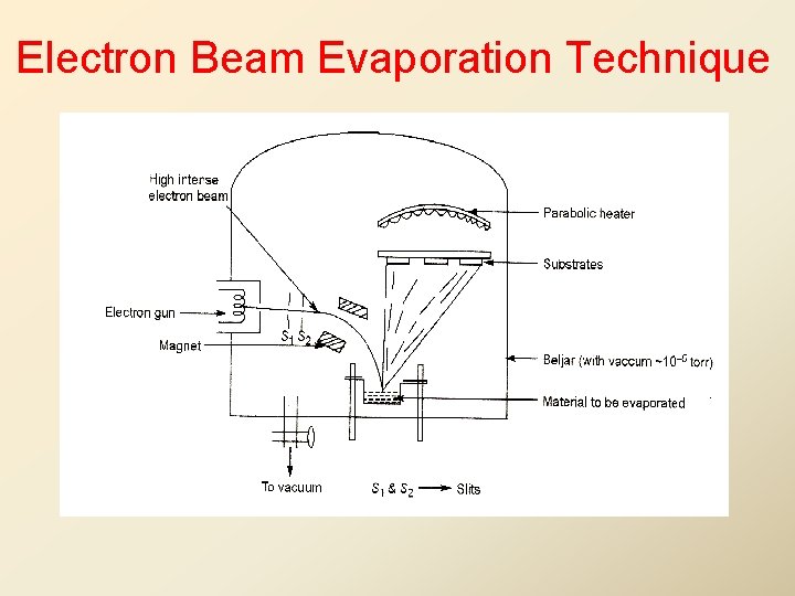
Electron Beam Evaporation Technique

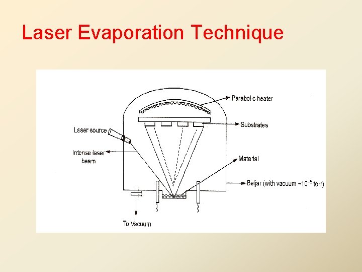
Laser Evaporation Technique

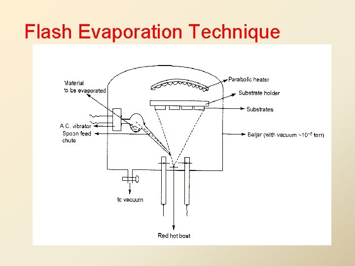
Flash Evaporation Technique

• • Examples of physical deposition: A thermal evaporator uses an electric resistance heater to melt the material and raise its vapor pressure to a useful range. This is done in a high vacuum, both to allow the vapor to reach the substrate without reacting with or scattering against other gas-phase atoms in the chamber, and reduce the incorporation of impurities from the residual gas in the vacuum chamber. Obviously, only materials with a much higher vapor pressure than the heating element can be deposited without contamination of the film. Molecular beam epitaxy is a particular sophisticated form of thermal evaporation. – An electron beam evaporator fires a high-energy beam from an electron gun to boil a small spot of material; since the heating is not uniform, lower vapor pressure materials can be deposited. – The beam is usually bent through an angle of 270° in order to ensure that the gun filament is not directly exposed to the evaporant flux. – Typical deposition rates for electron beam evaporation range from 1 to 10 nanometers per second. Sputtering relies on a plasma (usually a noble gas, such as Argon) to knock material from a "target" a few atoms at a time. The target can be kept at a relatively low temperature, since the process is not one of evaporation, making this one of the most flexible deposition techniques. It is especially useful for compounds or mixtures, where different components would otherwise tend to evaporate at different rates. Pulsed laser deposition systems work by an ablation process. Pulses of focused laser light vaporize the surface of the target material and convert it to plasma; this plasma usually reverts to a gas before it reaches the substrate. 9

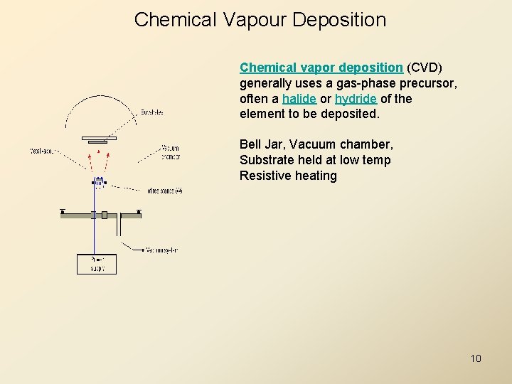
Chemical Vapour Deposition Chemical vapor deposition (CVD) generally uses a gas-phase precursor, often a halide or hydride of the element to be deposited. Bell Jar, Vacuum chamber, Substrate held at low temp Resistive heating 10

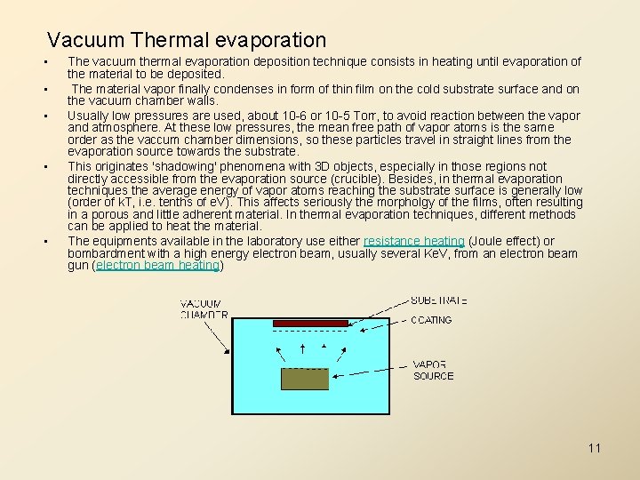
Vacuum Thermal evaporation • • • The vacuum thermal evaporation deposition technique consists in heating until evaporation of the material to be deposited. The material vapor finally condenses in form of thin film on the cold substrate surface and on the vacuum chamber walls. Usually low pressures are used, about 10 -6 or 10 -5 Torr, to avoid reaction between the vapor and atmosphere. At these low pressures, the mean free path of vapor atoms is the same order as the vaccum chamber dimensions, so these particles travel in straight lines from the evaporation source towards the substrate. This originates 'shadowing' phenomena with 3 D objects, especially in those regions not directly accessible from the evaporation source (crucible). Besides, in thermal evaporation techniques the average energy of vapor atoms reaching the substrate surface is generally low (order of k. T, i. e. tenths of e. V). This affects seriously the morpholgy of the films, often resulting in a porous and little adherent material. In thermal evaporation techniques, different methods can be applied to heat the material. The equipments available in the laboratory use either resistance heating (Joule effect) or bombardment with a high energy electron beam, usually several Ke. V, from an electron beam gun (electron beam heating) 11

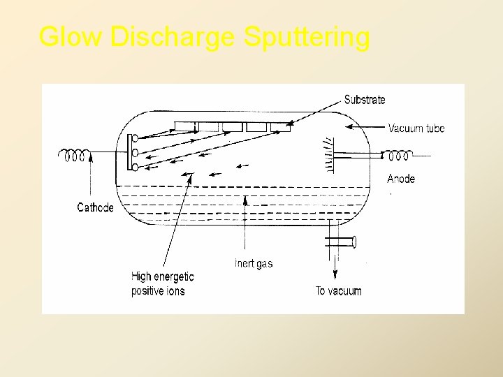
• 2. Sputtering: A technique used to deposit thin films of a material onto a surface. By first creating a gaseous plasma and then accelerating the ions from this plasma into some source material, the source material is eroded by the arriving ions via energy transfer and is ejected in the form of neutral particles - either individual atoms, clusters of atoms or molecules. As these neutral particles are ejected they will travel in a straight line unless they come into contact with something - other particles or a nearby surface. If a "substrate" such as a Si wafer is placed in the path of these ejected particles it will be coated by a thin film of the source material. 12

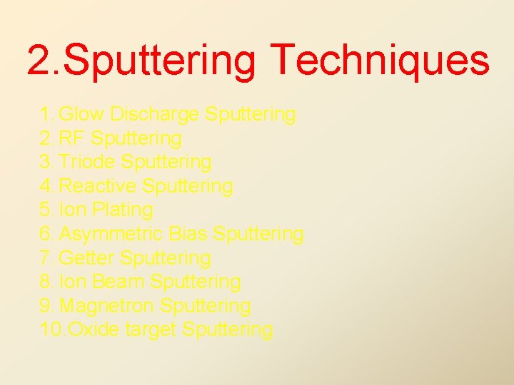
2. Sputtering Techniques 1. Glow Discharge Sputtering 2. RF Sputtering 3. Triode Sputtering 4. Reactive Sputtering 5. Ion Plating 6. Asymmetric Bias Sputtering 7. Getter Sputtering 8. Ion Beam Sputtering 9. Magnetron Sputtering 10. Oxide target Sputtering

Glow Discharge Sputtering

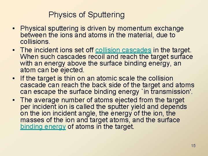
Physics of Sputtering • Physical sputtering is driven by momentum exchange between the ions and atoms in the material, due to collisions. • The incident ions set off collision cascades in the target. When such cascades recoil and reach the target surface with an energy above the surface binding energy, an atom can be ejected. • If the target is thin on an atomic scale the collision cascade can reach the back side of the target and atoms can escape the surface binding energy `in transmission'. • The average number of atoms ejected from the target per incident ion is called the sputter yield and depends on the ion incident angle, the energy of the ion, the masses of the ion and target atoms, and the surface binding energy of atoms in the target. 15

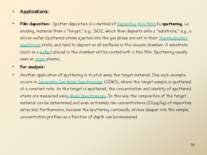
• Applications: • Film deposition: Sputter deposition is a method of depositing thin films by sputtering, i. e. eroding, material from a "target, " e. g. , Si. O 2, which then deposits onto a "substrate, " e. g. , a silicon wafer. Sputtered atoms ejected into the gas phase are not in their thermodynamic equilibrium state, and tend to deposit on all surfaces in the vacuum chamber. A substrate (such as a wafer) placed in the chamber will be coated with a thin film. Sputtering usually uses an argon plasma. • For analysis: • Another application of sputtering is to etch away the target material. One such example occurs in Secondary Ion Mass Spectroscopy (SIMS), where the target sample is sputtered at a constant rate. As the target is sputtered, the concentration and identity of sputtered atoms are measured using Mass Spectroscopy. In this way the composition of the target material can be determined and even extremely low concentrations (20 µg/kg) of impurities detected. Furthermore, because the sputtering continually etches deeper into the sample, concentration profiles as a function of depth can be measured. 16

Alloys • An alloy is a partial or complete solid solution of one or more elements in a metallic matrix. Complete solid solution alloys give single solid phase microstructure, while partial solutions give two or more phases that may be homogeneous in distribution depending on thermal (heat treatment) history. Alloys usually have different properties from those of the component elements. • Alloying one metal with other metal(s) or non metal(s) often enhances its properties. For instance, steel is stronger than iron, its primary element. The physical properties, such as density, reactivity, Young's modulus, and electrical and thermal conductivity, of an alloy may not differ greatly from those of its elements, but engineering properties, such as tensile strength and shear strength may be substantially different from those of the constituent materials. This is sometimes due to the sizes of the atoms in the alloy, since larger atoms exert a compressive force on neighboring atoms, and smaller atoms exert a tensile force on their neighbors, helping the alloy resist deformation. • Some alloys are made by melting and mixing two or more metals. Brass is an alloy made from copper and zinc. Bronze, used for bearings, statues, ornaments and church bells, is an alloy of copper and tin. 17

• Unlike pure metals, most alloys do not have a single melting point. Instead, they have a melting range in which the material is a mixture of solid and liquid phases. The temperature at which melting begins is called the solidus and the temperature when melting is complete is called the liquidus. • However, for most alloys there is a particular proportion of constituents which give them a single melting point or (rarely) two. This is called the alloy's eutectic mixture. • In practice, some alloys are used so predominantly with respect to their base metals that the name of the primary constituent is also used as the name of the alloy. For example, 14 karat gold is an alloy of gold with other elements. Similarly, the silver used in jewelry and the aluminium used as a structural building material are also alloys. • The term "alloy" is sometime used in everyday speech as a synonym for a particular alloy. For example, automobile wheels made of aluminium alloy are commonly referred to as simply "alloy wheels". The usage is obviously indefinite, since steels and most other metals in practical use are also alloys. 18

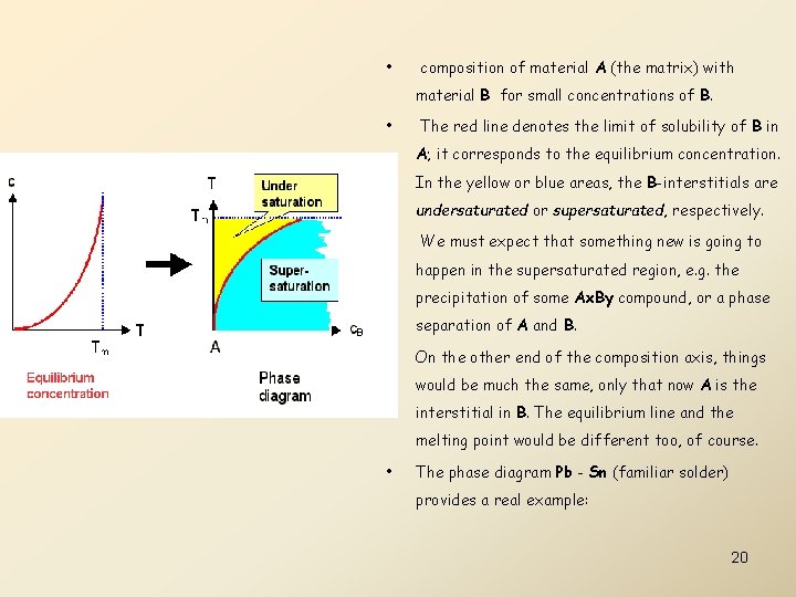
Phase Diagram • Phase diagrams are the map in temperature - composition space that shows the particular structure with the minimum free enthalpy at any point of the "map". • If we take the formula for the equilibrium concentration of self-interstitials to also describe the equilibrium concentration of extrinsic interstitial atoms if we replace the formation enthalpy by a corresponding property (lets call it solubility enthalpy), the resulting diagram of the equilibrium concentration over temperature can be interpreted as part of a phase diagram. • All we have to do is to switch the axes from the normal representation concentration vs. temperature to 19 temperature vs. concentration:

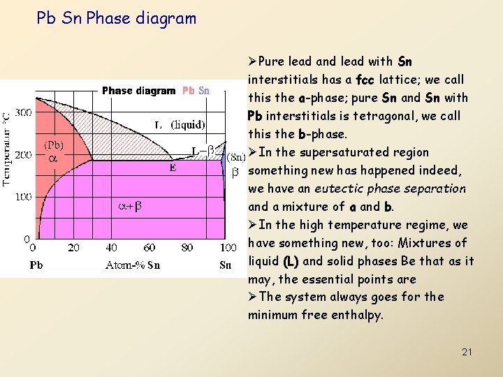
• composition of material A (the matrix) with material B for small concentrations of B. • The red line denotes the limit of solubility of B in A; it corresponds to the equilibrium concentration. In the yellow or blue areas, the B-interstitials are undersaturated or supersaturated, respectively. • We must expect that something new is going to happen in the supersaturated region, e. g. the precipitation of some Ax. By compound, or a phase separation of A and B. • On the other end of the composition axis, things would be much the same, only that now A is the interstitial in B. The equilibrium line and the melting point would be different too, of course. • The phase diagram Pb - Sn (familiar solder) provides a real example: 20

Pb Sn Phase diagram ØPure lead and lead with Sn interstitials has a fcc lattice; we call this the a-phase; pure Sn and Sn with Pb interstitials is tetragonal, we call this the b-phase. ØIn the supersaturated region something new has happened indeed, we have an eutectic phase separation and a mixture of a and b. ØIn the high temperature regime, we have something new, too: Mixtures of liquid (L) and solid phases Be that as it may, the essential points are ØThe system always goes for the minimum free enthalpy. 21

• • • Pure lead and lead with Sn interstitials has a fcc lattice; we call this the a-phase; pure Sn and Sn with Pb interstitials is tetragonal, we call this the b-phase. In the supersaturated region something new has happened ndeed, we have an eutectic phase separation and a mixture of a and b. In the high temperature regime, we have something new, too: Mixtures of liquid (L) and solid phases Be that as it may (and it can be much more complicated), the essential points are The system always goes for the minimum free enthalpy, and this minimum could be calculated in principle following the same, albeit much more involved line of reasoning we employed for equilibrium concentrations of point defects. The (experimentally determined) phase diagrams are maps of the particular minimum free enthalpy configuration out of many possible arrangements for a given composition and temperature. Changing the temperature or the composition of a system thus takes us from one area in the phase diagram to another; the boundaries we have to cross give us an idea of what has to happen kinetically. 22