Purpose of the Thin Film Technology Thin Films


 2. 表面擴散 (Surface Diffusion) Need energy 3. 分子-分子及基板-分子鍵結形成(化學性吸附) 4. 成核(Nucleation): aggregation")


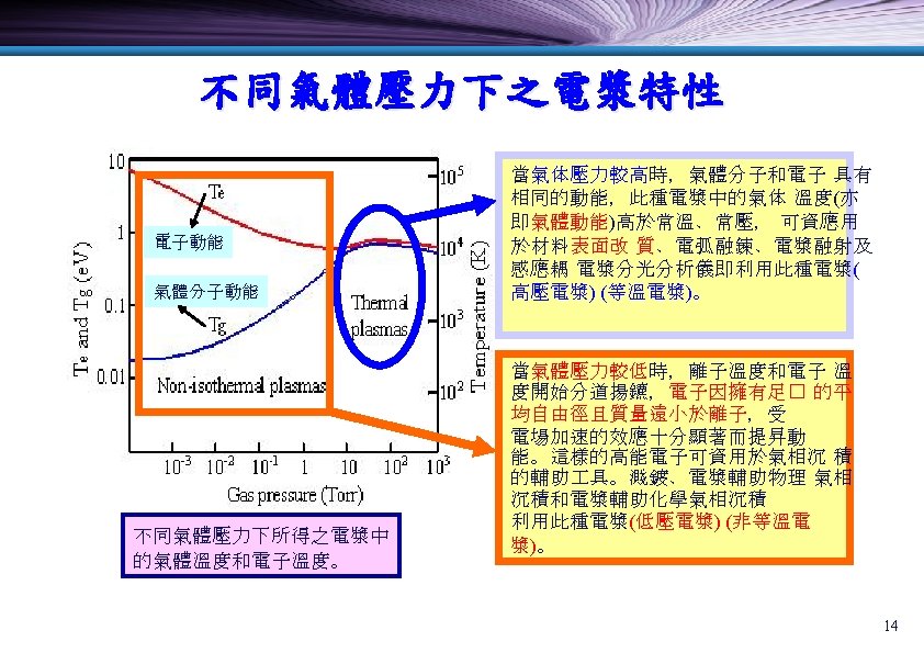
 E<10 e. V, ion可能被material表面吸附, 而以熱方式釋放能量. (2) E>10 Ke.")
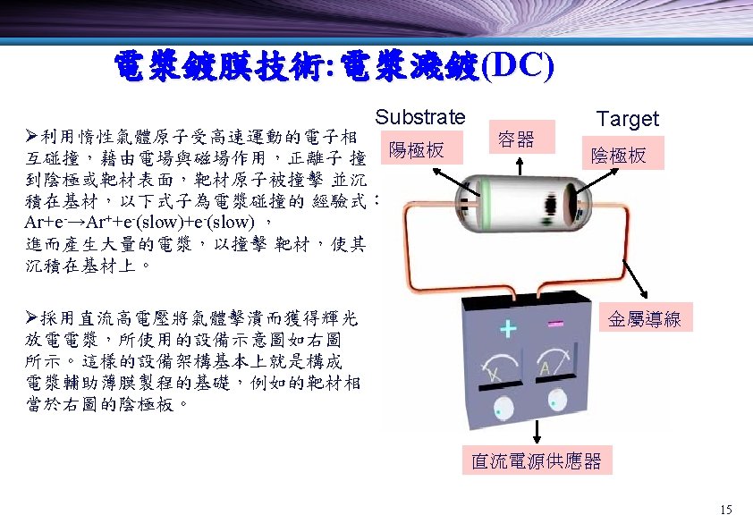
 (glow discharge) Cathode shield Schematic diagram of DC powered")


 32")


 : low particle contamination Cathode design")


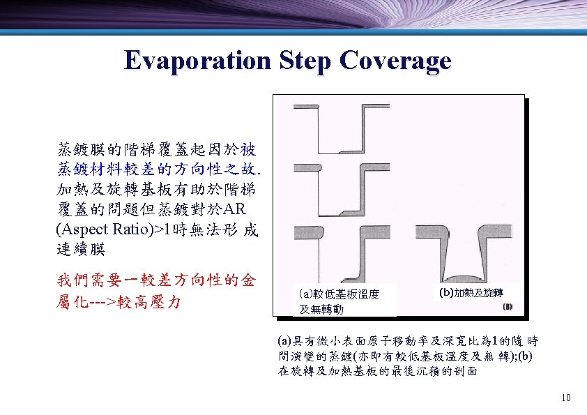
- Slides: 70
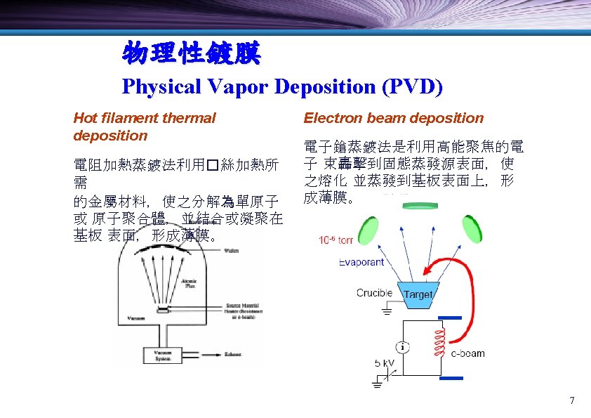
Purpose of the Thin Film Technology ØThin Films are deposited onto bulk material (Sub. ) to achieve properties unattainable or not easily attainable in the substrate alone. ØWhat properties are required for the application at hand? 3
Thin-Film Applications 4
薄膜成長基本步驟 1. 原子/分子的吸收(物理性吸收) 2. 表面擴散 (Surface Diffusion) Need energy 3. 分子-分子及基板-分子鍵結形成(化學性吸附) 4. 成核(Nucleation): aggregation of single atoms/molecules 5. 結構及微結構形成(amorphous, polycrystalline, single crystal, defects, roughness, etc…) 6. 膜本體內部之改變(diffusion, grain growth, etc. ) 5
How to Obtain the Thin Films • Poly-Si deposition • Epi-Si deposition • Dielectrics (Si. O 2 , Si 3 N 4 , Ti 2 O 5 ) deposition • Metals (Al-Cu, Ti. N, W, Cu, Ta. N) deposition Chemical vapor deposition (CVD) A(g)+B(g) →C(s) ↓+D(g) Physical vapor deposition (PVD) A(s) →A(g) →A(s) 6
Metallization Structure Semiconductor industry uses PVD to deposit the metal that electrically connects the various parts of the IC to each other and to the outside world. There are four common structures in metallization: contacts, vias, plugs and interconnects. Via 2 Interconnects Metal 3 Silicon Dioxide (ILD) Metal 2 Via 1 Silicon Dioxide (ILD) Metal 1 Silicon Dioxide Contact Silicon 8
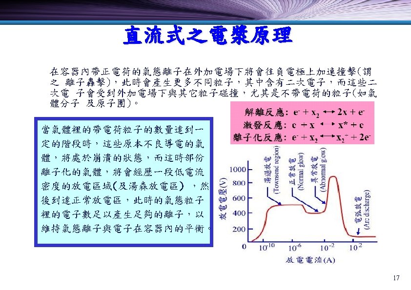
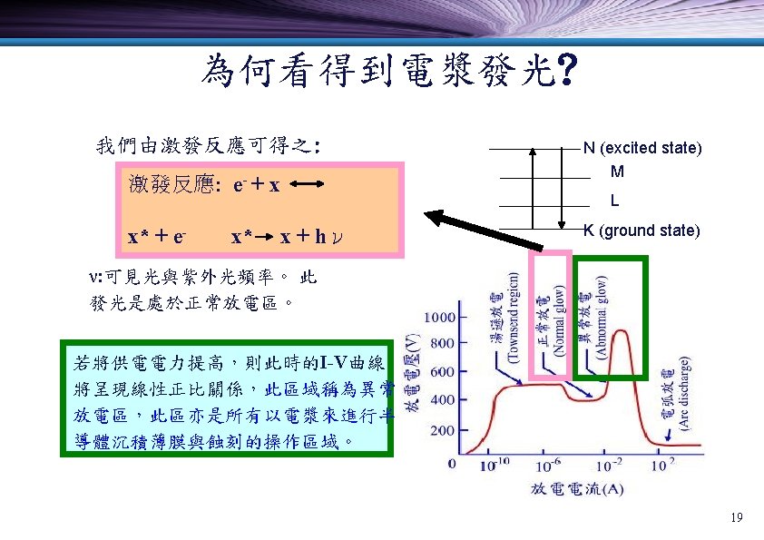
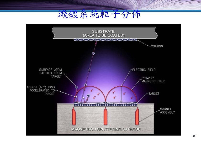
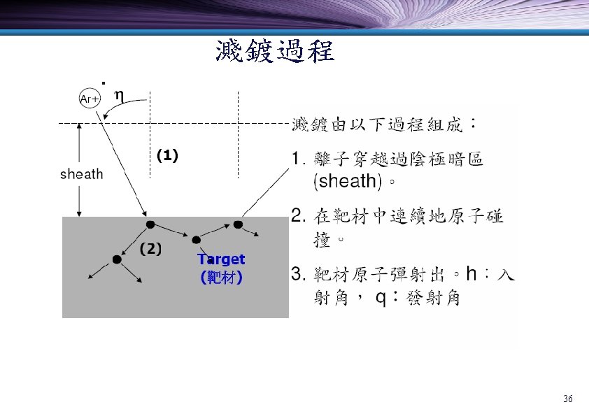
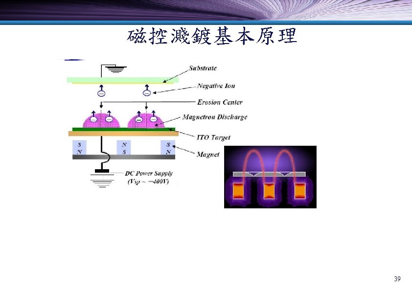
直流式之電漿原理 *當帶有能量之ions撞擊surface of material, 將發生以下四種cases. (1) E<10 e. V, ion可能被material表面吸附, 而以熱方式釋放能量. (2) E>10 Ke. V ion penetrates into the material many atomic large spacing, most of its energy deep into the substrate, where it changes the physical structure. (ion implantation). (3)若能量介於 10 e. V <E< 10 Ke. V, 則將有兩種energy transfer mechanisms 發生. (a) Part of the ion energy is deposited in the form of heat. (b) Remainder goes into a physical rearrangement of the substrate. ions將與target表面很多層原子互相作用. target atoms and clusters of atoms 將被ejected from the surface of the target. (with 10 to 50 e. V; 此些大約有evaporated atoms之100倍以上的能量). 提供 sputtered atoms具有額外之surface mobility, 以致能停留在substarte表面 最低 能量位置. 被sputtering出來約95%為atomic, 其餘可能為diatomic molecules. 18
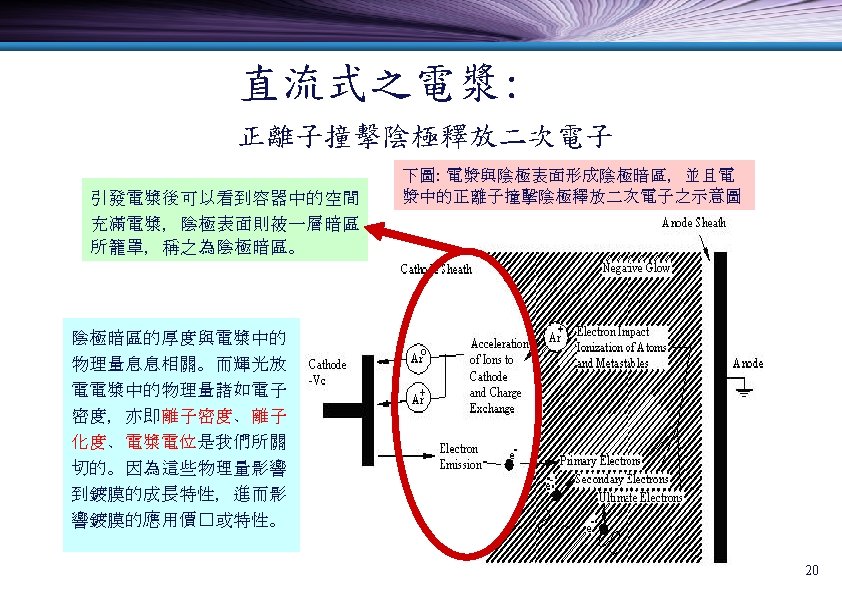
DC Sputter deposition -V (DC) (glow discharge) Cathode shield Schematic diagram of DC powered sputter deposition equipment Vacuum ground 22
DC Sputter system Plasma structure and voltage distribution Bulk of plasma contains equal con. of ions & electrons. Al, W, Ti, silicides, other metals Electric potential ~constant Voltage drop ~across the sheath regions. Plasma used in processing is a “weak” plasma, containing mostly neutral atoms/molecules (10 -3 to 10 -6) 23
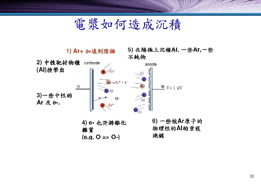
Processes in sputter deposition Al e- 只適用於導電材料 Power Supply 24
Sputtering yield in a DC system 25
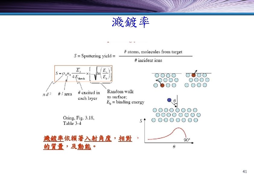
Sputtering yield in a DC system Defined as the number of atoms ejected per incident ion. Typically, range 0. 1 -3. Determines the deposition rate. Depends on: Target material. Mass of bombarding ions. Energy of the bombarding ions. Direction of incidence of ions (angle). 26
Contact hole filling problem Fort aspect ratios A = w/d smaller than approximately 1, the layer at the edge of the contact hole will become unacceptably thin or will even be non-existing - the contact to the underlying structure is not established. 27
Contact hole filling problem –– the real thing Real thing together with one way to overcome the problem is shown above (the example is from the 4 Mbit DRAM generation, around 1988). 28
RF sputter deposition Real thing together with one way to overcome the problem is shown above (the example is from the 4 Mbit DRAM generation, around 1988). 29
Reactive sputter deposition Real thing together with one way to overcome the problem is shown above (the example is from the 4 Mbit DRAM generation, around 1988). 30
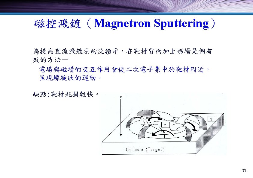
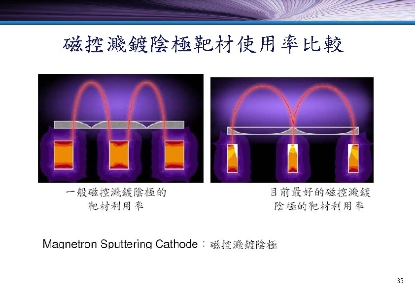
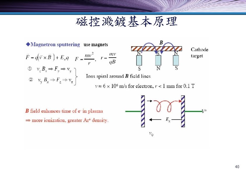
Magnetron sputter deposition 31
PVD -- (Sputtering deposition) 32
薄膜成長機制 Substrate 37
Sputtering Yield of Ar 42
Sputtering Yield of Ar 43
44
45
46
A 1 47
48
49
50
Bias sputtering • Sometimes bias sputtering of the wafer is desirable. This is done by reversing the electrical connections. • One application would be for precleaning the wafer before the actual deposition. • During this step, a controlled thickness of surface material is sputtered off the wafer, removing any contaminants or native oxide. • A film can then be sputter deposited immediately afterward without breaking the vacuum. 51
Bias sputtering • Useful for cleaning contact/vias. • Sputter etching has serious problems as particles. 52
Thermal Dissipation is not good. 53
54
55
56
57
58
59
D e p o s i t i o n R a t Data From ITRI 60
Reaction Process Models of Ir. O 2 Films by Reactive Sputtering 61
Reaction Process Models of Ir. O 2 Films by Reactive Sputtering 62
Substrate Temp. effect on the Ir. O 2 Resitivity 63
X R D p a t t e r n s o f I r 64
Manufacturing methods Thin film Equipment Al Magnetron sputter Ti and Ti. W Magnetron Ti. N Reactive sputtering Cu Typical reaction Comments 25 -300 C – standard 440 -550 C – hot Al Ti + N 2 (in plasma) Electroplating ÞTi. N Cu 2+ + 2 e- ÞCu 65
I T O S p u t t e r i n g ( i Applications of Sputtering 66
In-Line ITO Design Vertical substrate orientation ( 85°) : low particle contamination Cathode design : high deposition rate, low resistivity ITO and metal Heater design : homogeneous substrate temperature distribution Flexibility : ITO and others (Si. O 2 , Cr, Mo, Ti, Ta, . . ) using the same architecture 67
• 4 t h G e n e r a t i o n : M 4 th ITO Sputtering System 68
Sputtering for Components 69