Surface MEMS MEMS 2 Chapter 29 sami franssilaaalto

- Slides: 34

Surface MEMS (MEMS 2) (Chapter 29) sami. franssila@aalto. fi

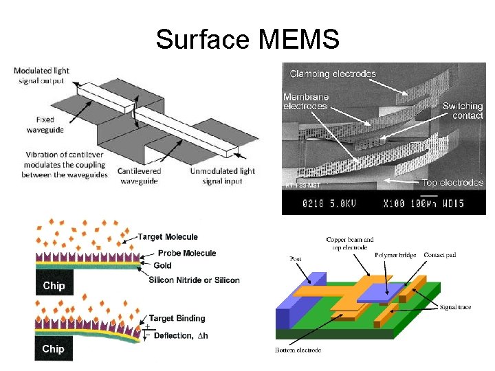
Surface MEMS

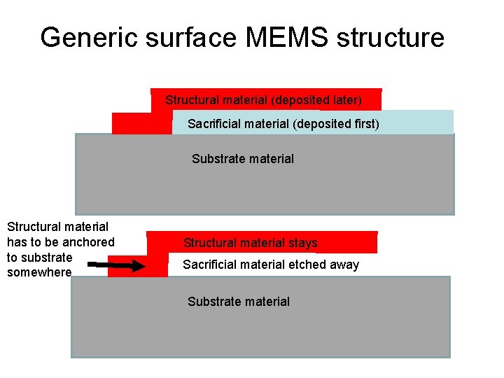
Generic surface MEMS structure Structural material (deposited later) Sacrificial material (deposited first) Substrate material Structural material has to be anchored to substrate somewhere Structural material stays Sacrificial material etched away Substrate material

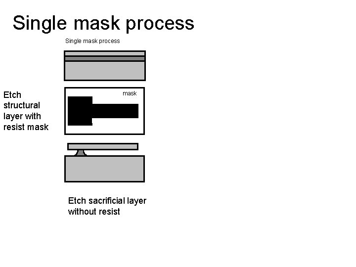
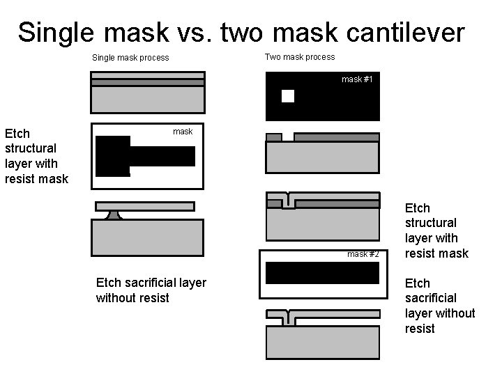
Single mask process Two mask process Single mask process mask #1 Etch structural layer with resist mask #2 Etch sacrificial layer without resist Etch structural layer with resist mask Etch sacrificial layer without resist

Single mask vs. two mask cantilever Two mask process Single mask process mask #1 Etch structural layer with resist mask #2 Etch sacrificial layer without resist Etch structural layer with resist mask Etch sacrificial layer without resist

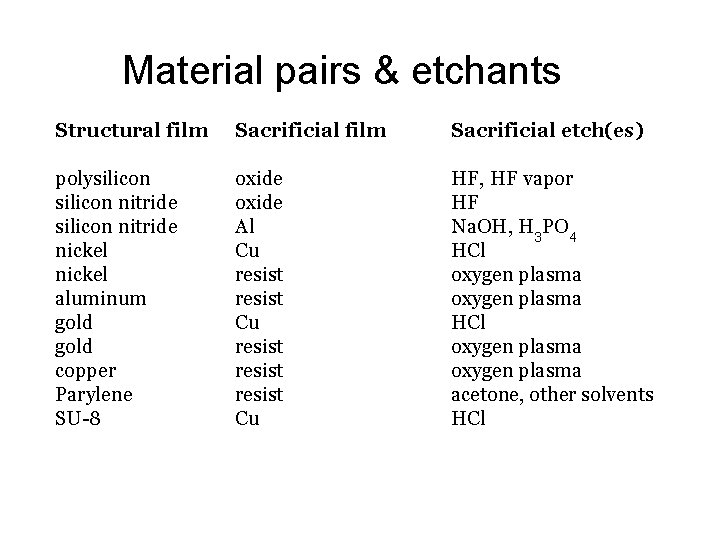
Material pairs & etchants Structural film Sacrificial etch(es) polysilicon nitride nickel aluminum gold copper Parylene SU-8 oxide Al Cu resist resist Cu HF, HF vapor HF Na. OH, H 3 PO 4 HCl oxygen plasma acetone, other solvents HCl

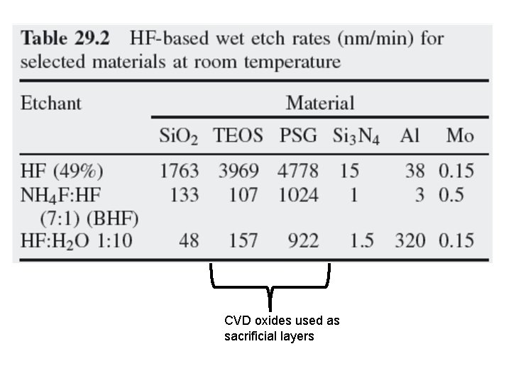
CVD oxides used as sacrificial layers

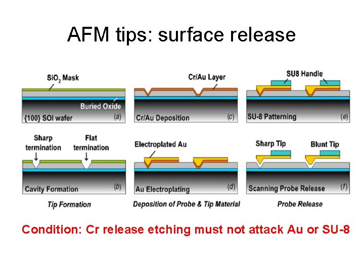
AFM tips: surface release Condition: Cr release etching must not attack Au or SU-8

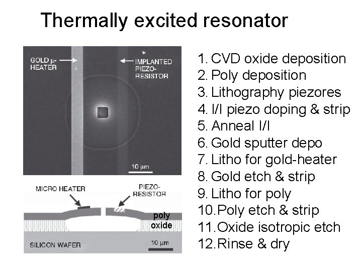
Thermally excited resonator poly oxide 1. CVD oxide deposition 2. Poly deposition 3. Lithography piezores 4. I/I piezo doping & strip 5. Anneal I/I 6. Gold sputter depo 7. Litho for gold-heater 8. Gold etch & strip 9. Litho for poly 10. Poly etch & strip 11. Oxide isotropic etch 12. Rinse & dry

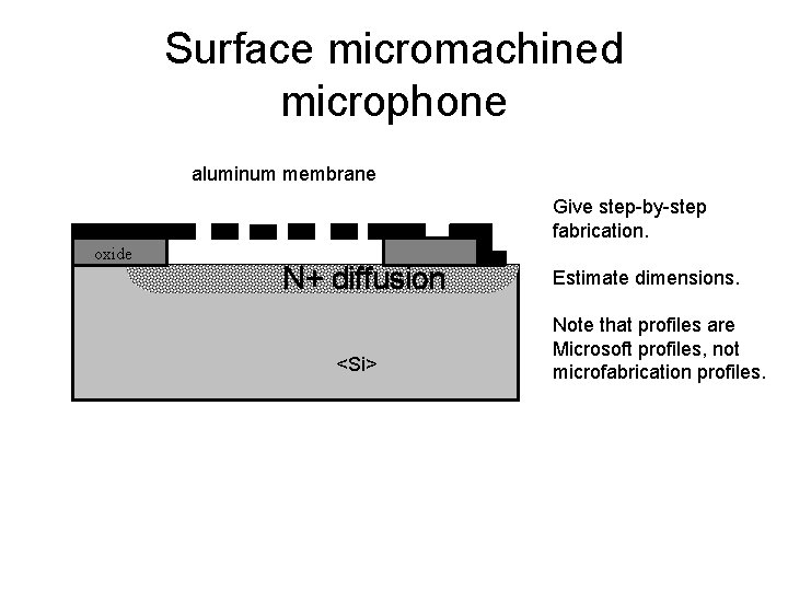
Surface micromachined microphone aluminum membrane Give step-by-step fabrication. oxide N+ diffusion <Si> Estimate dimensions. Note that profiles are Microsoft profiles, not microfabrication profiles.

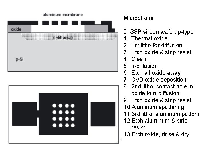
Microphone 0. SSP silicon wafer, p-type 1. Thermal oxide 2. 1 st litho for diffusion 3. Etch oxide & strip resist 4. Clean 5. n-diffusion 6. Etch all oxide away 7. CVD oxide deposition 8. 2 nd litho: contact hole in oxide to n-diffusion 9. Etch oxide & strip resist 10. Aluminum sputtering 11. 3 rd litho: aluminum pattern 12. Etch aluminum & strip resist 13. Etch oxide, rinse & dry

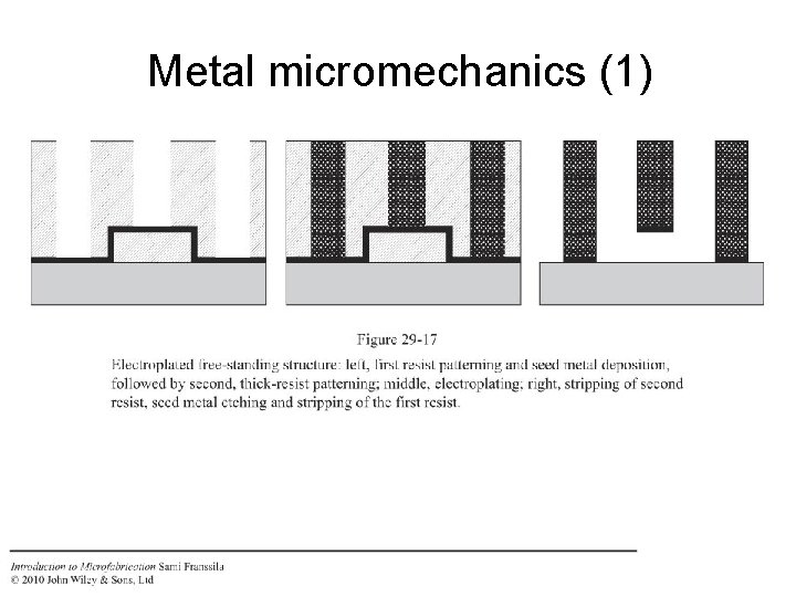
Metal micromechanics (1)

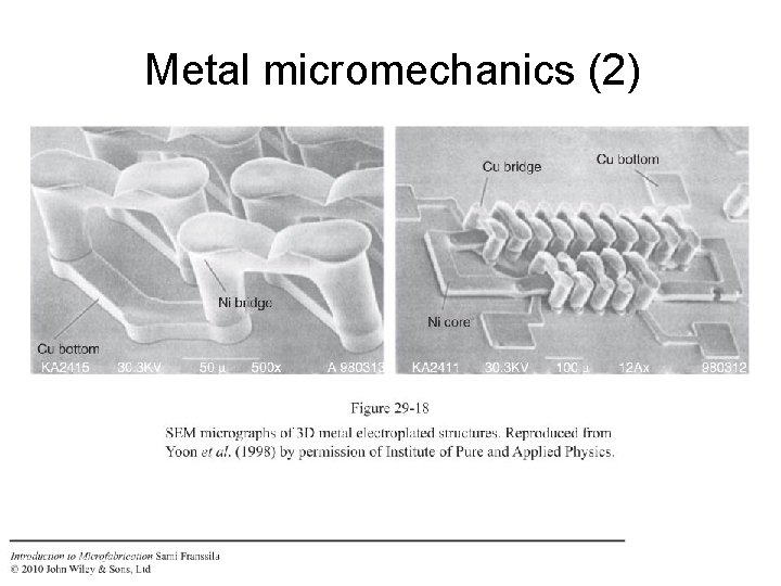
Metal micromechanics (2)

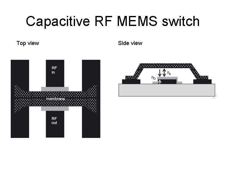
Capacitive RF MEMS switch Top view Side view

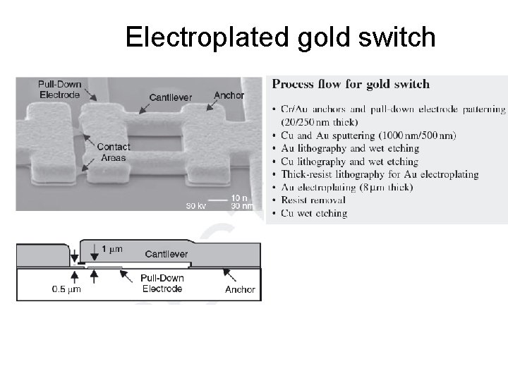
Electroplated gold switch

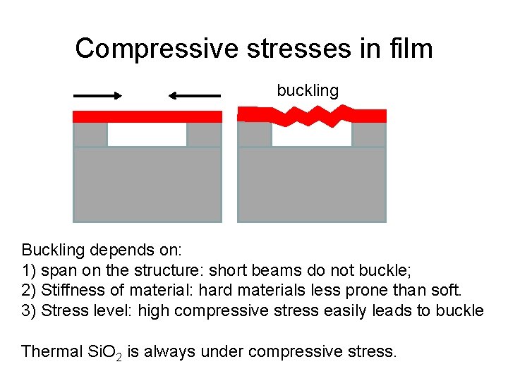
Compressive stresses in film buckling Buckling depends on: 1) span on the structure: short beams do not buckle; 2) Stiffness of material: hard materials less prone than soft. 3) Stress level: high compressive stress easily leads to buckle Thermal Si. O 2 is always under compressive stress.

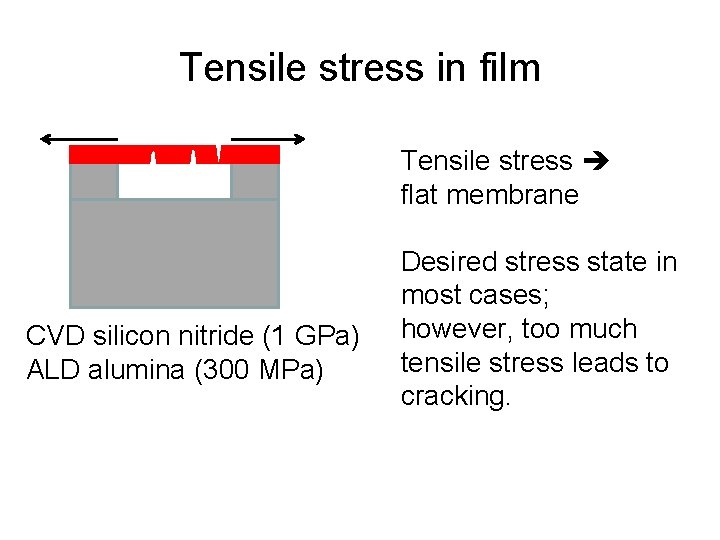
Tensile stress in film Tensile stress flat membrane CVD silicon nitride (1 GPa) ALD alumina (300 MPa) Desired stress state in most cases; however, too much tensile stress leads to cracking.

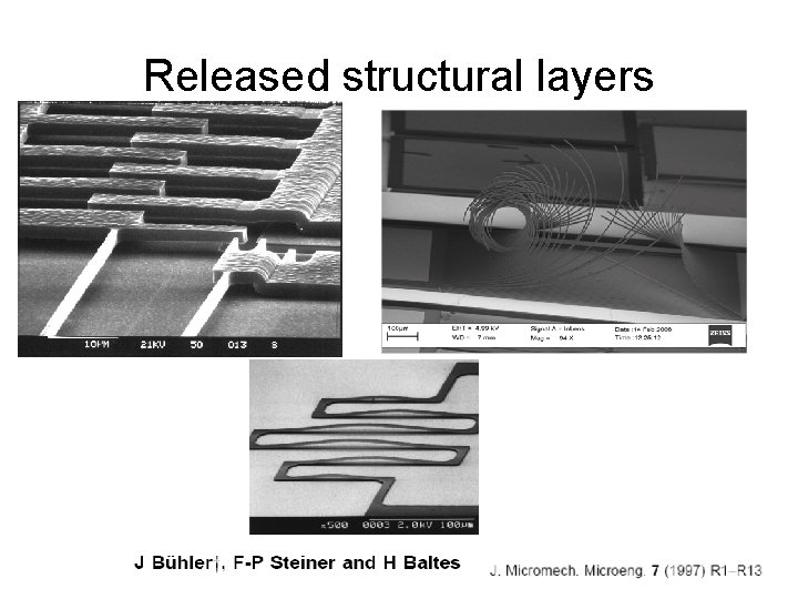
Released structural layers

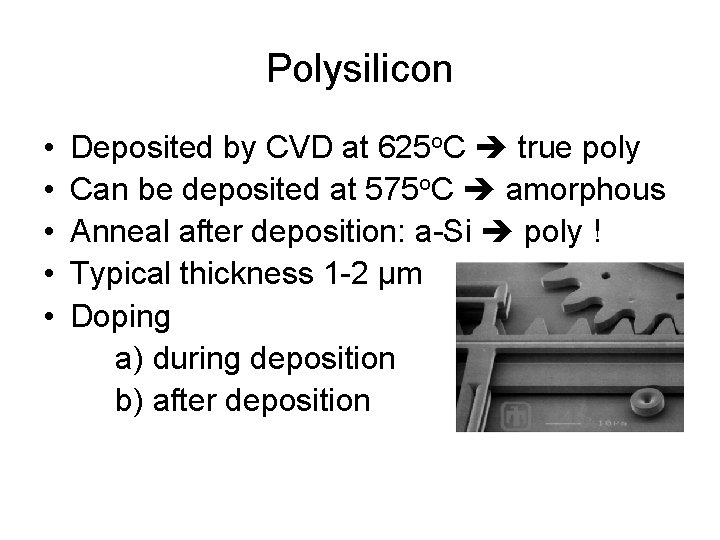
Polysilicon • • • Deposited by CVD at 625 o. C true poly Can be deposited at 575 o. C amorphous Anneal after deposition: a-Si poly ! Typical thickness 1 -2 µm Doping a) during deposition b) after deposition

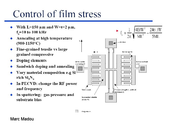
Polysilicon doping • Usually deposited undoped (practically insulator) • Doping after deposition – diffusion – implantation • • Annealing ~950 o. C, 1 h to activate dopants Annealing changes film stress (and grain size) Heavy doping ca. 500 µΩ-cm (cf. Al 3 µ Ω-cm ) Grain size ca. 200 -300 nm after anneal

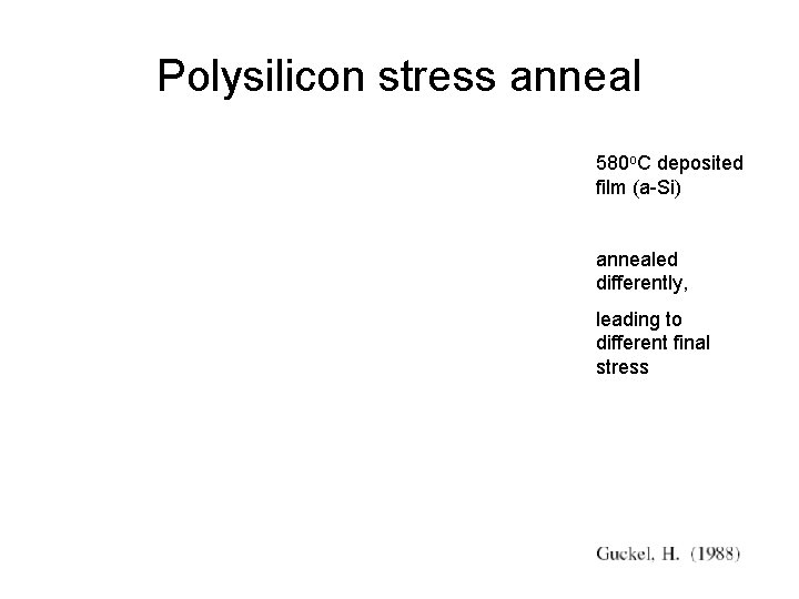
Polysilicon stress anneal 580 o. C deposited film (a-Si) annealed differently, leading to different final stress

Marc Madou

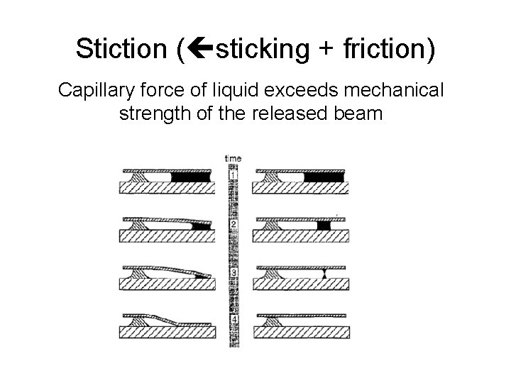
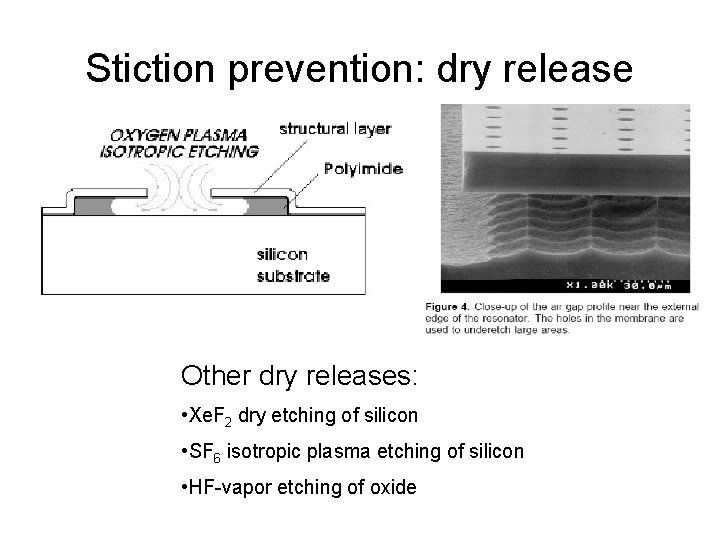
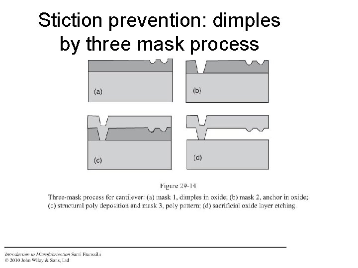
Stiction ( sticking + friction) Capillary force of liquid exceeds mechanical strength of the released beam

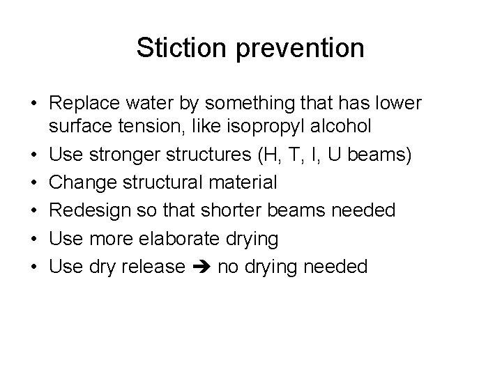
Stiction prevention • Replace water by something that has lower surface tension, like isopropyl alcohol • Use stronger structures (H, T, I, U beams) • Change structural material • Redesign so that shorter beams needed • Use more elaborate drying • Use dry release no drying needed

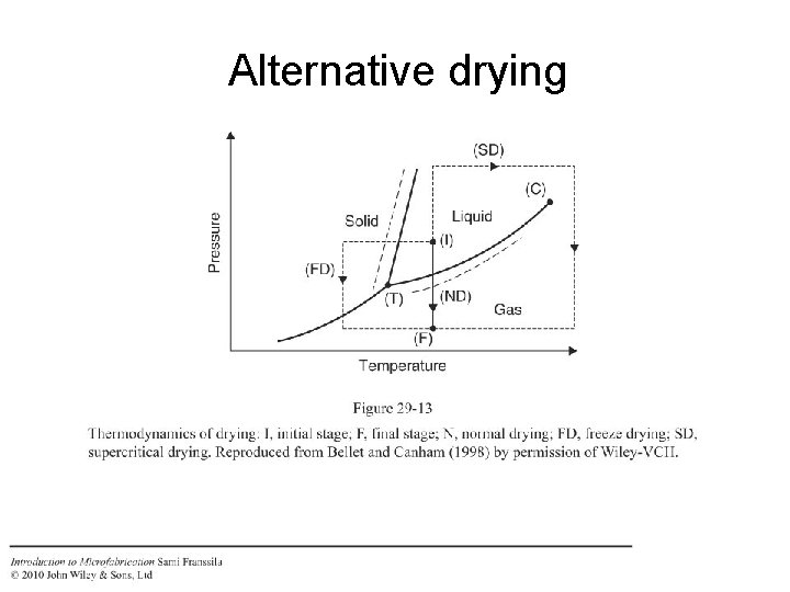
Alternative drying

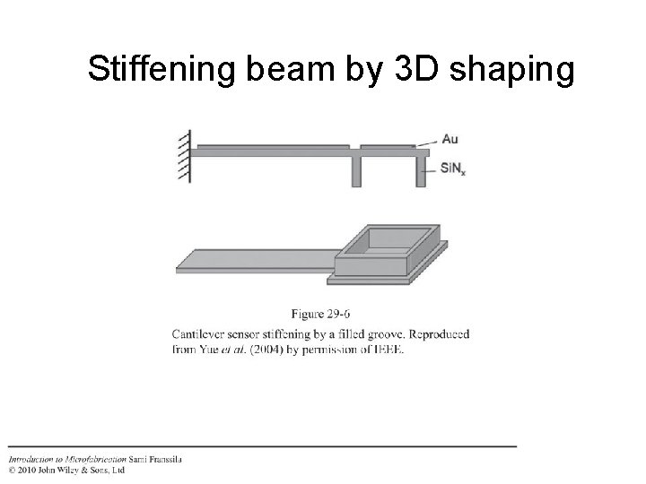
Stiffening beam by 3 D shaping

Stiction prevention: dry release Other dry releases: • Xe. F 2 dry etching of silicon • SF 6 isotropic plasma etching of silicon • HF-vapor etching of oxide

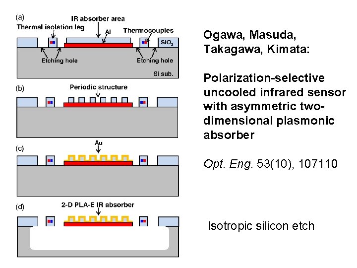
Ogawa, Masuda, Takagawa, Kimata: Polarization-selective uncooled infrared sensor with asymmetric twodimensional plasmonic absorber Opt. Eng. 53(10), 107110 Isotropic silicon etch

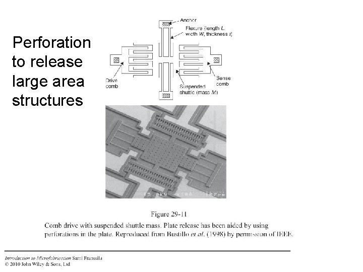
Perforation to release large area structures

Stiction prevention: dimples by three mask process

Types of MEMS Bulk MEMS: anisotropic wet or DRIE of bulk silicon SOI MEMS: DRIE or wet etching of SOI wafers Surface MEMS: thin films on top of a wafer Integrated MEMS: CMOS and MEMS on same chip

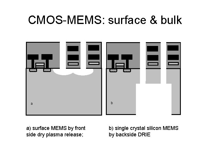
CMOS-MEMS: surface & bulk a a) surface MEMS by front side dry plasma release; b b) single crystal silicon MEMS by backside DRIE

CMOS-MEMS (2) If a fully processed CMOS wafer is used as a starting substrate for MEMS processing, what limitations are there ?

Surface MEMS