Scaling sami franssilaaalto fi Contents Wafer size scaling


 =")
: linewith/50 = gate oxide")

*6 nm +")


 does NOT scale; it has remained")


- Slides: 40
Scaling sami. franssila@aalto. fi
Contents Wafer size scaling Chip size scaling Wafer thickness scaling Projection lithography Etch scaling (from wet to dry) Selectivity scaling (CMOS gate) Gate oxide scaling Junction depth scaling Thermal budget scaling (RTA) Film thickness scaling (MLM, constant AR Fab size scaling Fab cost scaling. Linewidth scaling
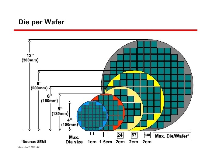
Wafer size scaling 525 µm 625 µm 775 µm ? ? 925 µm Wafer thickness scaling
Wafer size and demand Doering, R. & Y. Nishi: Limits of integrated circuit manufacturing, Proc. IEEE Vol. 89 (2001) p. 375
New prediction https: //www. extremetech. com/extreme/163372 -atom-everywhere-intelbreaks-ground-on-first-450 mm-fab
Useful chips & edge exclusion
Chip scaling and wafer scaling
Chip size vs. Yield Good Money chips USD 255 1020 98 1176 32 1696 18 1314 10 1490 6 1632 4 1668 EE 141 © Digital Integrated Circuits 2 nd Introduction 1 Digital Integrated Circuits A Design Perspective Introduction Jan M. Rabaey Anantha Chandrakasan.
Optical projection lithography Sources of radiation (UV 365 nm-436 nm, DUV 193 nm-248 nm, EUV, X-rays, electrons, ions) Optical system I (lenses, mirrors) Mask (pattern) Optical system II (lenses, mirrors) Numerical aperture NA=sin Imaging medium (resist) Wafer (with patterns) Wafer stage (alignment mechanism)
Reduction factor, often 5 X Mask 1 µm minimum linewidth 5 X optical reduction 0. 2 µm on wafer
Projection litho performance
Table 10. 1: Linewidth scaling of CMOS Wavelength Aperture k factor =436 nm NA=0. 38 k 1=0. 8 =365 nm NA=0. 48 k 1=0. 6 =248 nm NA=0. 60 k 1=0. 6 =248 nm NA=0. 65 k 1=0. 5 Linewidth Do. F 1 µm 0. 5 µm 0. 25 µm 0. 18 µm 1. 5µm 0. 8 µm 0. 35 µm 0. 30 µm Because depth of focus (Do. F) gets smaller, CMP planarization becomes more important all the time.
Projection lithography scaling Lin, MEMS 2010
Photomask cost scaling Min LW Cost 3 µm 1 µm 300 euros 500 euros 1000 euros, quality checked Mask LW Wafer LW Cost 1 µm 0. 5 µm 200 nm 100 nm 0. 2 µm 0. 1 µm 40 nm 2000 euros 5000 euros 20000 euros 50000 euros 1 X litho 5 X reduction litho
Refresher: etch profiles Wet etching isotropic profile Plasma etching anisotropic profile
Wet etched profile: 1 µm thick film 5 µm 3 µm 2 µm 1 µm
Plasma etched profile: 1 µm film 5 µm 3 µm 2 µm 1 µm
Wet etched profile: 200 nm film 5 µm 3 µm 2 µm 1 µm
Plasma etched profile: 200 nm film 5 µm 3 µm 2 µm 1 µm
Etch back Conformal deposition Anisotropic etch 200 nm/min for 1 minute. 200 nm 400 nm
Etch time, end point and overetch 300 nm 100 % conformal deposition. 200 nm Etch rate 100 nm/min. Anisotropic etch. Etch time 1 min. spacers formed Etch time 3 minutes; i. e. 2 minutes overetch (200%). Clears spacers.
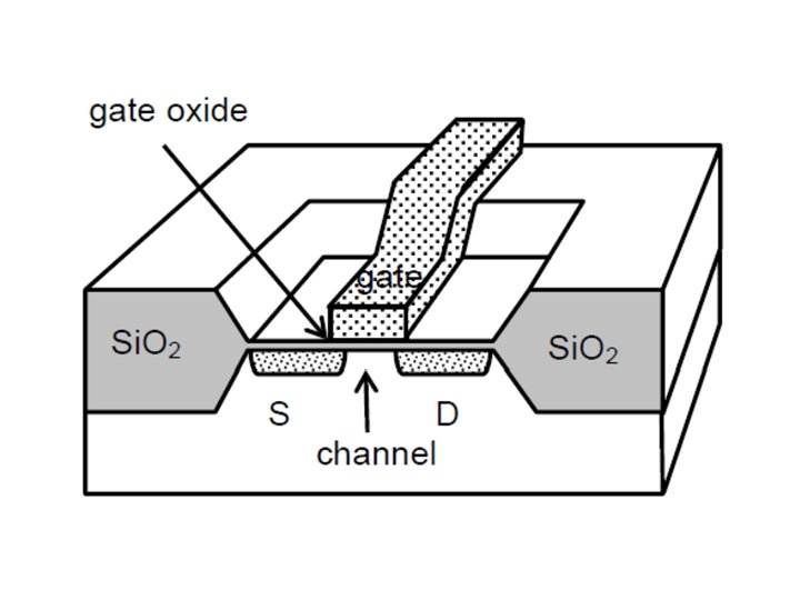
CMOS gate etch selectivity CMOS linewidth: 5 µm Polysilicon gate: 500 nm thick Gate oxide thickness (LW/50) = 100 nm Etch selectivity poly: oxide = 10: 1 Overetch = 50 % Oxide loss = nm Oxide loss = % of original thickness CMOS linewidth: 1 µm Polysilicon gate: 300 nm thick Gate oxide thickness (LW/50) = 20 nm Overetch = 50 % Oxide loss = same % loss as in above, Calculate etch selectivity poly: oxide needed to achieve this !
CMOS linewidth: 5 µm Polysilicon gate: 500 nm thick Gate oxide thickness (LW/50) = 100 nm Etch selectivity poly: oxide = 10: 1 Presume: 500 nm/min poly 50 nm/min oxide Overetch = 50 % 0. 5 min oxide etched Oxide loss = 25 nm Oxide loss = 25% of original thickness CMOS linewidth: 1 µm Polysilicon gate: 300 nm thick Gate oxide thickness (LW/50) = 20 nm Overetch = 50 % Oxide loss = same % loss as in above, Calculate etch selectivity poly: oxide needed! Presume 300 nm/min 50% oe is 30 secs 5 nm loss allowed 10 nm/min oxide rate 30: 1 selectivity needed
Gate oxide scaling Rule of thumb (valid for 1970 -2000): linewith/50 = gate oxide thickness 5 µm 100 nm 1 µm 20 nm 0. 5 µm 10 nm 0. 2 µm 4 nm 0. 1 µm 2 nm HERE WE RUN INTO PROBLEMS…
High-k dielectrics Zr. O 2 Hf. O 2 High dielectric constants of ca. 20 (vs. 4 for Si. O 2) Deposited by ALD. Si. O 2 formed in the first steps of ALD, because H 2 O used as a precursor.
Equivalent oxide thickness Example: 6 nm Zr. O 2: EOT = (4/23)*6 nm + 0 nm = 1 nm Si. O 2 + 6 nm Zr. O 2: EOT = (4/23)*6 nm + 1 nm = 2 nm
Junction depth scaling Thermal diffusion 300 nm deep 300 nm sideways vs. ion implantation 300 nm deep 100 nm sideways
CMOS S/D scaling 5 µm gate length 0. 5 µm S/D diffusion depth 4 µm Leffective 1. 5 µm gate length 0. 5 µm S/D diffusion depth 0. 5 µm Leffective
S/D scaling trick #1: implant energy down e. g. 50 ke. V B+ e. g. 10 ke. V B+ or 50 ke. V BF 2+ Sideways spreading is 1/3 of vertical depth, for both.
S/D scaling trick #2: spacers Anisotropic etching of a conformal film Ion implantation Leff = Lithographic !
Spacers and LDDs extended Energy X Energy scaled down narrow spacer enough.
Thermal budget scaling & RTA Ion implantation always requires a high temperature annealing step to get rid of implant damage. I/I damage anneal time is short compared with diffusion because only local movement of atoms needed, e. g. to move an interstitial atom into a lattice site. As S/D junction needs to be shallower, anneal thermal budget (T, t) needs to be scaled down. E. g. 1100 o. C & 30 secs 1100 o. C & 15 secs 1050 o. C & 15 secs but then 1200 o. C & 1 s 1200 o. C & 0. 1 sec
Sheet resistance scaling Rs /T I/I dose constant 1015 cm-2 Use simple box approximation in transforming dose to concentration S/D 1 µm deep 1019 cm-3 Rs = 0. 01 Ω-cm/10 -4 cm = 100 Ω S/D 0. 1 µm 1020 cm-3 0. 001 Ω-cm/10 -5 cm = 100 Ω
Aspect ratio scaling Actually, aspect ratio (height: width) does NOT scale; it has remained more or less 1: 1 for decades.
8 -level IC metallization
Fab cost scaling 1957 1967 1977 1987 1997 2007 2017 0. 2 M$ 2. 5 M$ 1000 M$ 3000 M$ ?
Fab size scaling Year Wafer size LW WPM* 1970 1980 1990 2000 2010 2020 3” 100 mm 150 mm 200 mm 300 mm 10 µm 2 µm 0. 8 µm 0. 18 µm 32 nm 11 nm 1000 5000 10000 20000 50000 70000 * Wafer starts per month
Wafer specifications for CMOS Wafer size 100 125 150 200 300 mm Thickness 525 675 725 775 µm TTV 3 3 2 1. 5 1 µm Warp 20 -30 18 -35 20 -30 10 -20 µm Flatness <3 <2 <1 0. 5 -0. 8 µm Oxygen 20 17 15 14 12 pmma OISF 100 -200 100 <10 none cm-2 Particles Particle size 10 0. 3 5 -10 0. 3 10 -100 0. 16 50 -100 0. 12 #/wafer µm Metal impurities 1012 1011 5*1010 109 atoms/cm 2