Oxidation and doping sami franssilaaalto fi Microfabrication 1

Oxidation and doping sami. franssila@aalto. fi Microfabrication 1
 Dry oxidation: Si (s) + O 2 (g)")
Thermal oxidation (at ~1000 o. C) Dry oxidation: Si (s) + O 2 (g) ==> Si. O 2 (s) Wet oxidation: Si (s) + 2 H 2 O (g) ==> Si. O 2 (s) + 2 H 2 (g) Original silicon surface

Videos • Thermal oxidation • https: //www. youtube. com/watch? v=nz. F 8 f 6 ocq. Xo TKK MICRONOVA, 2010 Microfabrication 3
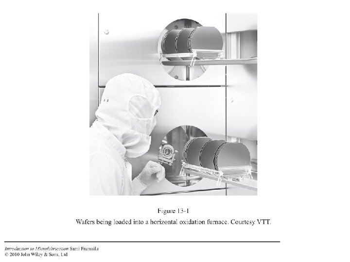

Oxidation furnace oxygen hydrogen burn box 3 -zone resistive heating nitrogen DCE/HCl

Oxidation is slow: 1000 nm is thick Parabolic rate law: thickness = constant * √time T/o. C

What happens to materials in oxygen at 1000 o. C ? -silicon -epitaxial silicon -polysilicon -amorphous silicon oxidized into Si. O 2 -silicon nitride: not affected -metals: melted (Al m. p. 653 C) -metals: oxidized (e. g. Cu. O) (==> not conductive any more) -metals: reacted with silicon (e. g. Ti. Si 2 , conductor) -polymers (e. g. resist): burned (CO 2; H 2 O)

Thermal oxide vs. CVD oxide O 2 gas in thermal, 1000 o. C silicon Si. H 4 + N 2 O gases in any wafer CVD 300 -900 o. C Compressive stress always, silicon consumed Stress can be tailored tensile or compressive, deposition also on metals
 • Nitride prevents oxygen diffusion oxidation areas defined by")
Local oxidation of silicon (LOCOS) • Nitride prevents oxygen diffusion oxidation areas defined by nitride lithography & etching nitride Si. O 2 nitride

More thermal oxide If there are both silicon and oxide areas exposed, oxidation will occur on both ! Microfabrication 10

Uses of oxide • etch mask material in MEMS silicon etching • diffusion mask in boron/phosphorous doping • electrical insulator • thermal insulator • hydrophilic surface • sacrificial material to be etched away

Oxide as sacrificial material Si. O 2 poly Si. O 2 Isotropic HF wet etching of oxide under polysilicon Membrane is released and can move (=vibrate according to thermal expansion induced by heating the gold wire) H. G. Craighead

Oxide-silicon interface
 + O 2 (g) ==> Si. O 2 (s)")
Oxidation of polysilicon Si (s) + O 2 (g) ==> Si. O 2 (s)
 or n-type (phosphorous-doped most often) The whole wafer")
Wafers always come doped p-type (boron-doped) or n-type (phosphorous-doped most often) The whole wafer is doped with same dopant concentration. Typically 1015 -1016 cm-3 dopants. Silicon atom density is 5*1022 cm-3. If we want to locally modify doping, we can add dopants (but never reduce !)
 phosporous (opposite dopant always present)")
Silicon substrate (p-type with boron majority) phosporous (opposite dopant always present)

Phosphorous diffusion top layer turned into n-type boron phosporous Bulk of the wafer remains p-type, diffused layer ~ µm only.

Very few dopant atoms needed ! Dopant atoms penetrate in silicon (some stopped inside mask oxide). For every dopant atom there are millions of silicon atoms. Dopant concentration decreases rapidly as a function of depth.
 Transition from n-type")
Junction depth, xj : change of doping type N-type (phosphorous majority) Transition from n-type to p-type = xj P-type (boron majority) boron phosporous

Junction depth xj Cdopant 1020 cm-3 xj ≈ 1. 2 µm 1018 cm-3 1016 cm-3 0. 5 1. 0 1. 5 depth/µm Xj is the depth where diffused dopant concentration equals wafer dopant concentration (of opposite type).

Time evolution of diffusion depth: x≈√Dt Lateral spreading equal to depth 1 hour 1 µm 4 hours 2 µm 9 hours 3 µm decreasing dopant concentration Microfabrication Slowly increasing depth 21

Doping technologies Gas phase diffusion Solid source diffusion Ion implantation e. g. POCl 3 gas e. g. boron-doped 20 -200 ke. V ions at 1000 o. C polysilicon film at room temperature at 1000 o. C Oxide mask Resist mask

Videos • Doping refresher: • https: //www. youtube. com/watch? v=k 12 GMjt. N 8 a. A TKK MICRONOVA, 2010 Microfabrication 23

Doping vs. resistivity Polysilicon less conductive than single crystal silicon with same dopant concentration (because grain boundaries limit charge carriers) Poly resistivity depends on details of deposition process.
 interstitial b) substitutional/vacancy c) interstitialcy.")
Diffusion mechanisms a) interstitial b) substitutional/vacancy c) interstitialcy.
, dose (1014 cm-2), energy (100 ke.")
Ion implantation: Projected range and straggle Ion (P), dose (1014 cm-2), energy (100 ke. V) Straggle Projected range 150 nm Microfabrication 26

Implant parameters Acceleration voltage 10 -200 k. V Ion energies 10 -200 ke. V Implant depths 10 -500 nm Doses 1011 to 1016 ions/cm-2. Concentrations ca. 1015 cm-3 to 1020 cm-3. 5. 1015 cm-2 ion implant dose and depth of ca. 200 nm translates to ca. 25 Ohm/sq sheet resistance Microfabrication 27

Implanted dopant profiles Light ions penetrate deeper Energetic ions penetrate deeper 50 ke. V 100 ke. V 150 ke. V
 inside silicon")
Implantation thru oxide Dopant ion max. concentration Implantation through oxide is (deep) inside silicon (not possible by diffusion)

Annealing after implantation • implantation is a room temperature process • silicon crystal is damaged by high energy ions • this damage is annealed away at ca. 1000 o. C • implantation always requires high temperature just like thermal diffusion (but easier process sequence by elimination of oxide)
 cause mainly point")
Implantation damage Light ions like boron, and low doses (<1014 cm-2) cause mainly point defects High doses (>1015 cm-2) and heavy ions (As+, Sb+, Ge+) cause extended damage and amorphization Microfabrication 31

Implant damage, anneal, diffusion, activity implant damage electrical activity dopant solubility dopant diffusivity Annealing at ca. 1000 o. C is always needed after implantation. TKK MICRONOVA, 2010 Microfabrication 32

Two modes of diffusion Fixed supply of dopant: when dopant atoms diffuse into silicon, surface concentration decreases. Infinite supply of dopant: New supply of dopant keeps surface concentration constant when dopant atoms diffuse into silicon. For example: Ion implantation is used to introduce dopant into surface layer of silicon, e. g. 1014 cm-2 dose. Phosphorous-doped CVD oxide film (500 nm thick, 5% P corresponds to 25 nm thick phosphorous layer) is a source that is practically unlimited (because only one atom in a million is dopant atom, 25 nm of phosphorous could dope 25 millimeters of <Si>. When wafer is brought to ca. 1000 o. C, dopant atoms diffuse deeper into silicon. If depth is 1 µm (10 -4 cm), conc. is 1018 cm-3. Microfabrication 33

Fixed source Infinite source Surface conc. down Surface conc. constant Substrate doping level Increasing time e. g. ion implanted region Increasing time Substrate doping level e. g. doped thin film

Doping level Wafers always come doped: 1013 -1020 cm-3 of dopant. Diffusion and implantation add dopants doped region dopant concentration always higher than original wafer. P-type 1017 cm-3 P-type 1015 cm-3 N-type 1017 cm-3 Possible Impossible by diffusion/implantation Microfabrication 35

Doping with epitaxial layers P-type 1018 cm-3 P-type 1016 cm-3 P-type 1018 cm-3 Epitaxy is the only way to get this. vs. N-type 1015 cm-3 Epitaxy is a good way to get this when thick doped layer is needed or when uniform dopant profile is needed. Microfabrication 36

Epitaxial layer vs. diffused layer P-type 1017 cm-3 P-type 1014 cm-3 vs. N-type 1014 cm-3 Diffusion doping Epitaxy Original silicon surface Microfabrication 37

Multiple diffusions p diffusion n-silicon n-diff 1019 cm-3 p diffusion 1017 cm-3 n-silicon 1015 cm-3 N-diff concentration must be higher than p-diff; otherwise dopant type does not change. 1. Take n-type silicon wafer 2. Thermal oxidation 3. Lithography 4. Oxide mask etching 5. Perform p-diffusion 6. Etch oxide away 7. Thermal oxidation 8. Lithography 9. Oxide etching 10. n-diffusion & p-diffusion becomes deeper Microfabrication 38

MOS-controlled thyristor Multiple diffusions: -deep p diffusion -heavy n+ diffusion -intermediate n diffusion -shallow p+ diffusion -heavy p+ diffusion on back Microfabrication 39

CMOS source/drain doping Doping by diffusion: Oxide mask for diffusion MOS gate needs to be aligned to S/D junctions Self-aligned gate by implantation: polysilicon gate blocks ions, and MOS channel remains undoped. Source/drain regions automatically aligned to gate. misalignment Microfabrication 40

Implantation vs. diffusion • Implantation is more accurate in dose control • Implantation produces greater variety of profiles • Implantation is possible through oxide and nitride • • • Thick oxide, nitride and poly will block implanted ions Sideways spreading in diffusion ≈ depth Sideways spreading in implantation is ≈ 1/3 depth Diffusion is high-temperature process needs oxide or nitride mask Implantation is room temperature process resist mask But: damages after implantation are annealed at high temperature both need ca. 1000 o. C • Diffusion is the best for high doping level, deep junctions and double side doping Microfabrication 41
 Shallowest last (p+) It is")
Order of diffusions? P-epi layer growth Deepest first (NWELL) Shallowest last (p+) It is possible to do lithoimplant-litho-implant, and one annealing step to cure the damage and drive the dopants deeper, e. g. medium depth n+ and p+ in the figure could be combined this way. US 6297070 B 1 Microfabrication 42
- Slides: 42