Surface MEMS sami franssilaaalto fi Applications Generic structure
- Slides: 36

Surface MEMS sami. franssila@aalto. fi

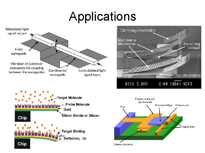
Applications

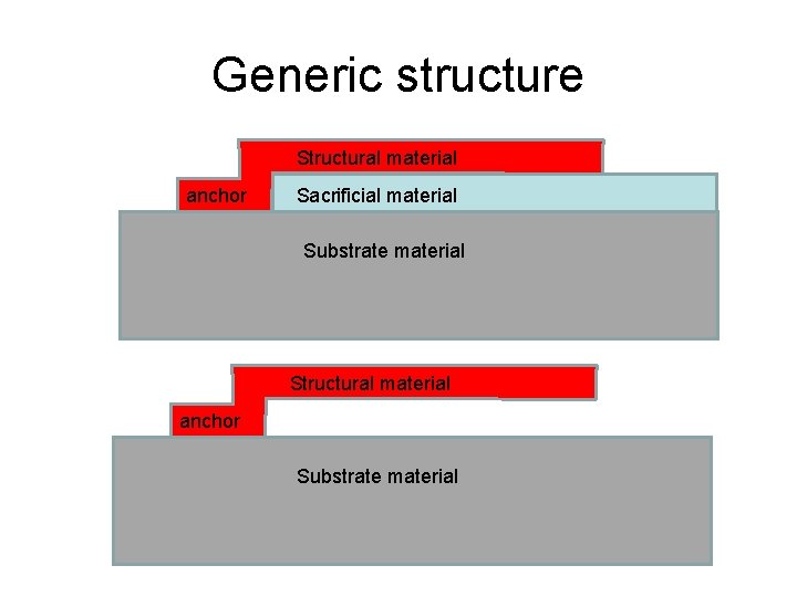
Generic structure Structural material anchor Sacrificial material Substrate material Structural material anchor Substrate material

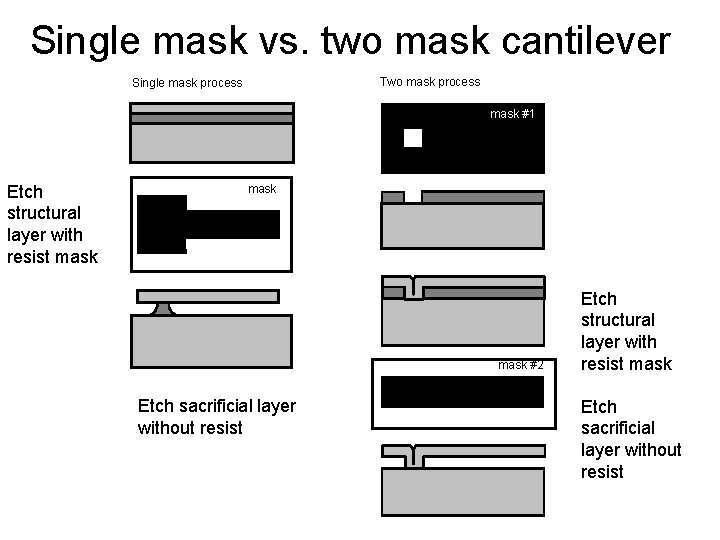
Single mask vs. two mask cantilever Two mask process Single mask process mask #1 Etch structural layer with resist mask #2 Etch sacrificial layer without resist Etch structural layer with resist mask Etch sacrificial layer without resist

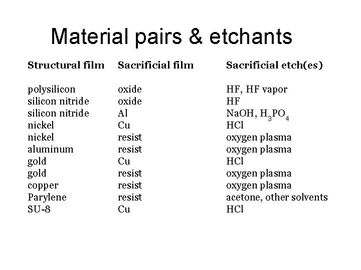
Material pairs & etchants Structural film Sacrificial etch(es) polysilicon nitride nickel aluminum gold copper Parylene SU-8 oxide Al Cu resist resist Cu HF, HF vapor HF Na. OH, H 3 PO 4 HCl oxygen plasma acetone, other solvents HCl

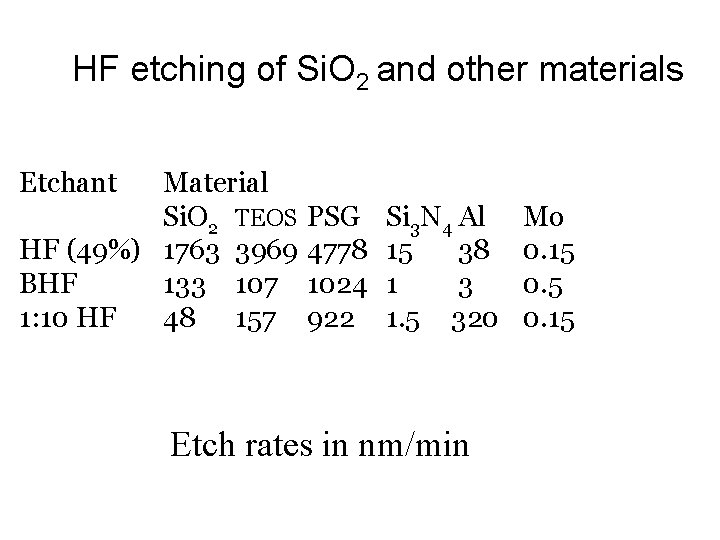
HF etching of Si. O 2 and other materials Etchant Material Si. O 2 TEOS HF (49%) 1763 3969 BHF 133 107 1: 10 HF 48 157 PSG 4778 1024 922 Si 3 N 4 Al 15 38 1 3 1. 5 320 Etch rates in nm/min Mo 0. 15

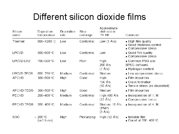
Different silicon dioxide films

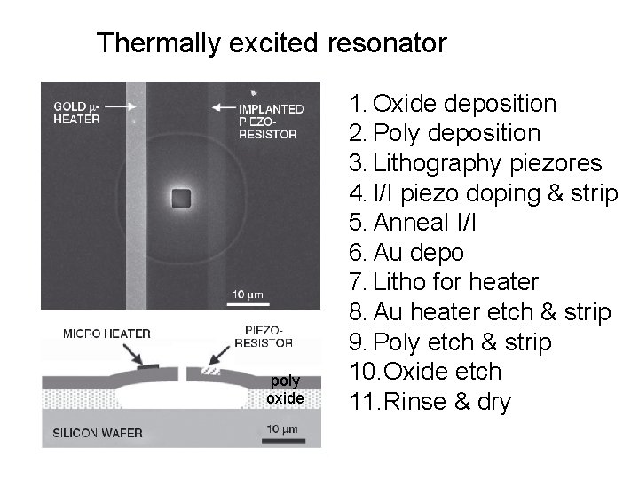
Thermally excited resonator poly oxide 1. Oxide deposition 2. Poly deposition 3. Lithography piezores 4. I/I piezo doping & strip 5. Anneal I/I 6. Au depo 7. Litho for heater 8. Au heater etch & strip 9. Poly etch & strip 10. Oxide etch 11. Rinse & dry

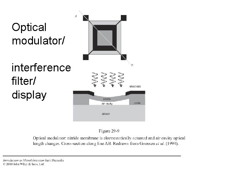
Optical modulator/ interference filter/ display

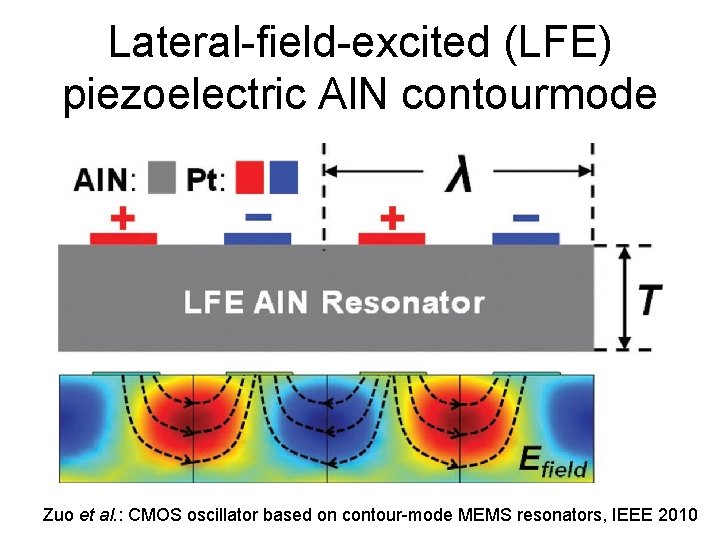
Lateral-field-excited (LFE) piezoelectric Al. N contourmode Zuo et al. : CMOS oscillator based on contour-mode MEMS resonators, IEEE 2010

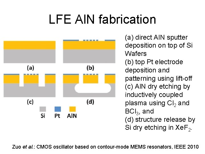
LFE Al. N fabrication (a) direct Al. N sputter deposition on top of Si Wafers (b) top Pt electrode deposition and patterning using lift-off (c) Al. N dry etching by inductively coupled plasma using Cl 2 and BCl 3, and (d) structure release by Si dry etching in Xe. F 2. Zuo et al. : CMOS oscillator based on contour-mode MEMS resonators, IEEE 2010

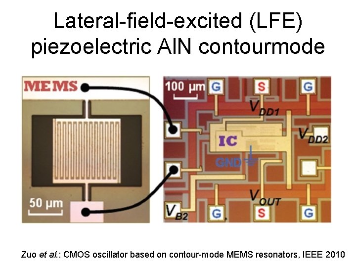
Lateral-field-excited (LFE) piezoelectric Al. N contourmode Zuo et al. : CMOS oscillator based on contour-mode MEMS resonators, IEEE 2010

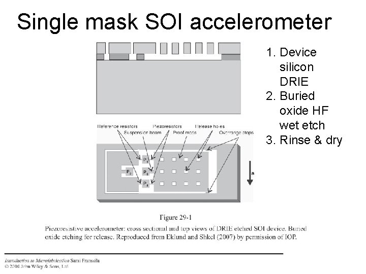
Single mask SOI accelerometer 1. Device silicon DRIE 2. Buried oxide HF wet etch 3. Rinse & dry

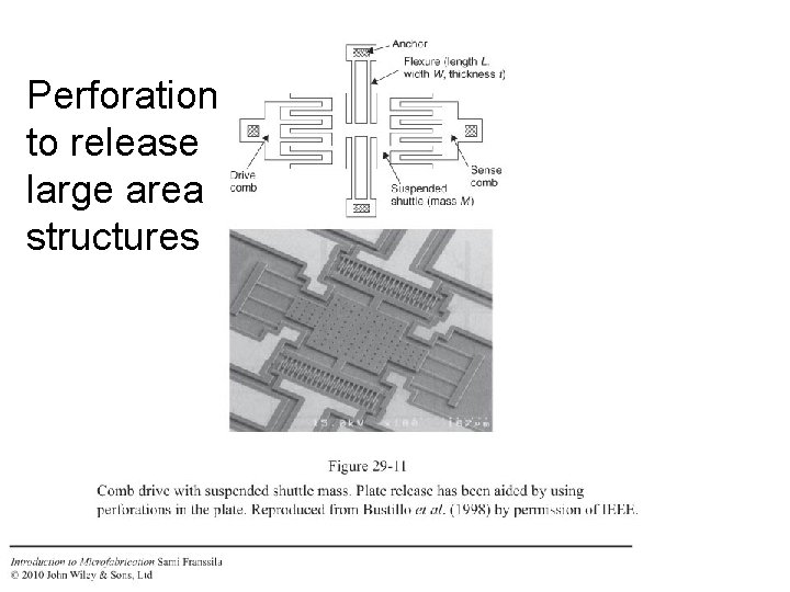
Perforation to release large area structures

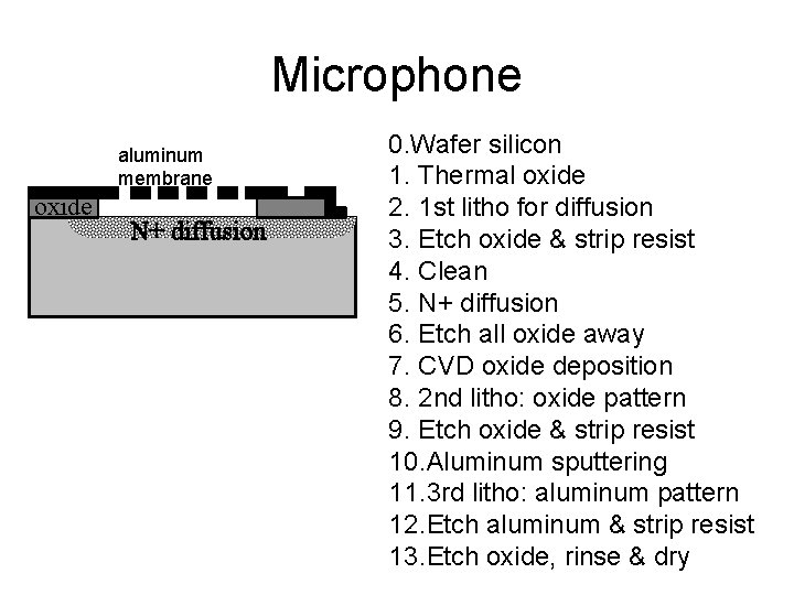
Microphone aluminum membrane oxide N+ diffusion 0. Wafer silicon 1. Thermal oxide 2. 1 st litho for diffusion 3. Etch oxide & strip resist 4. Clean 5. N+ diffusion 6. Etch all oxide away 7. CVD oxide deposition 8. 2 nd litho: oxide pattern 9. Etch oxide & strip resist 10. Aluminum sputtering 11. 3 rd litho: aluminum pattern 12. Etch aluminum & strip resist 13. Etch oxide, rinse & dry

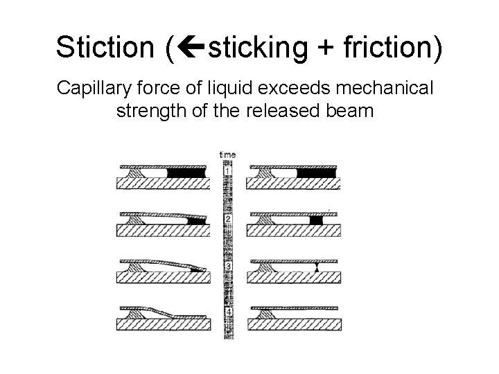
Stiction ( sticking + friction) Capillary force of liquid exceeds mechanical strength of the released beam

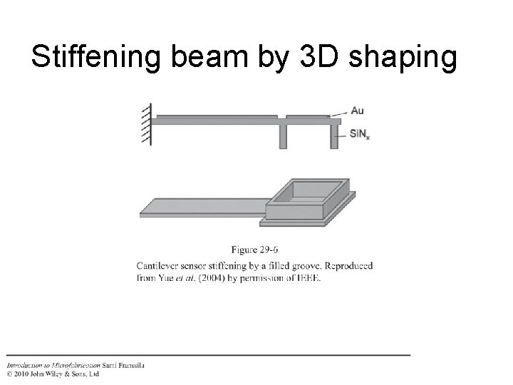
Stiffening beam by 3 D shaping

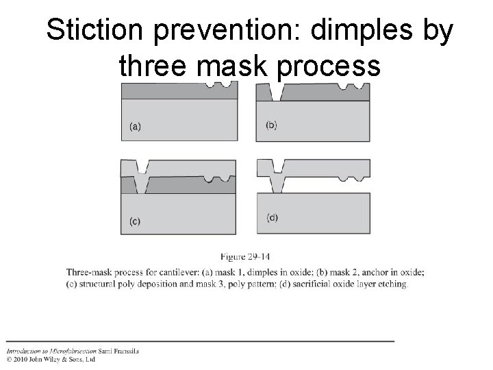
Stiction prevention: dimples by three mask process

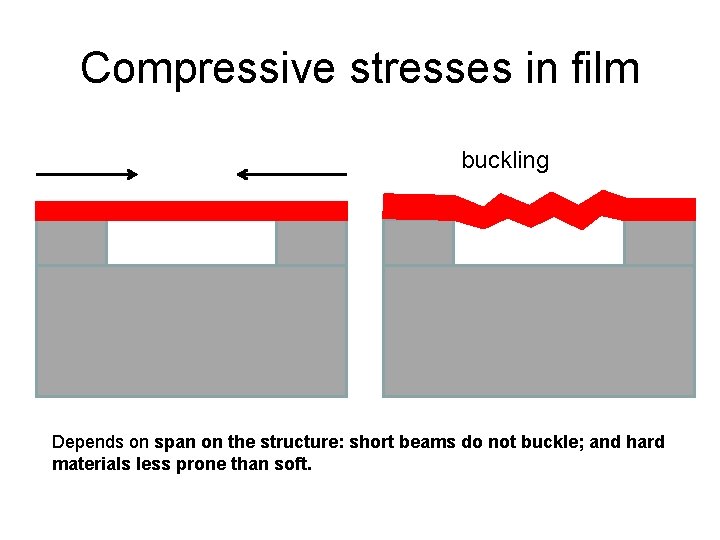
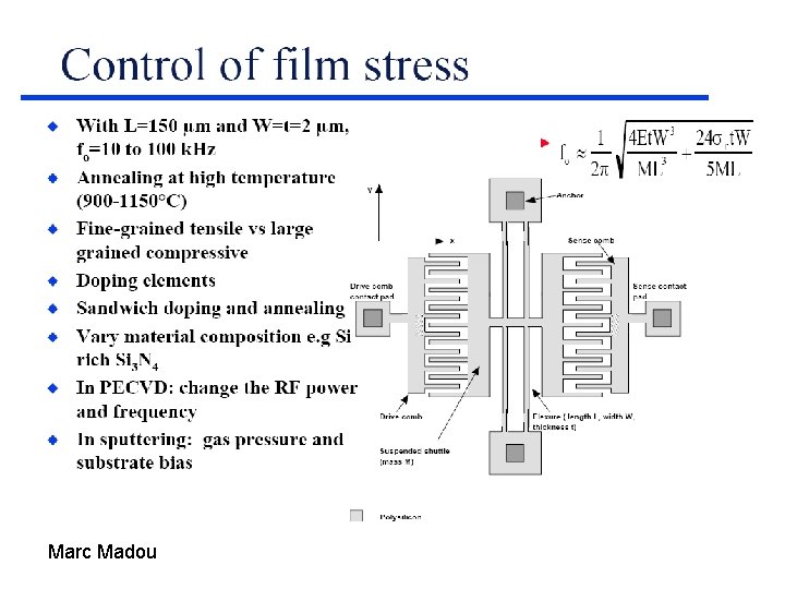
Compressive stresses in film buckling Depends on span on the structure: short beams do not buckle; and hard materials less prone than soft.

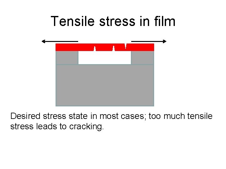
Tensile stress in film Desired stress state in most cases; too much tensile stress leads to cracking.

Marc Madou

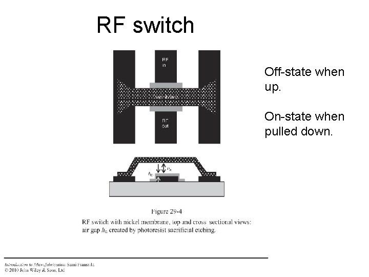
RF switch Off-state when up. On-state when pulled down.

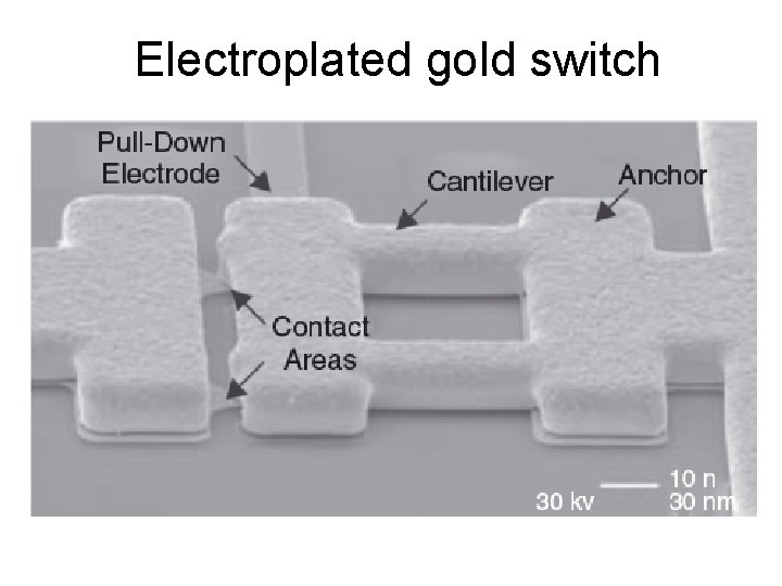
Electroplated gold switch

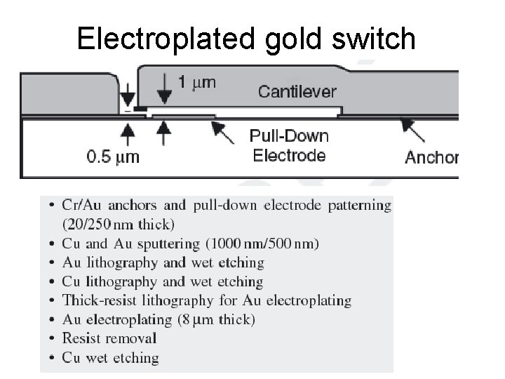
Electroplated gold switch

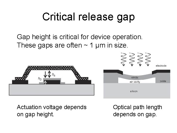
Critical release gap Gap height is critical for device operation. These gaps are often ~ 1 µm in size. Actuation voltage depends on gap height. Optical path length depends on gap.

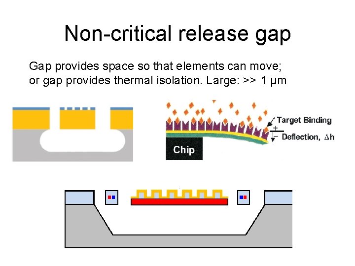
Non-critical release gap Gap provides space so that elements can move; or gap provides thermal isolation. Large: >> 1 µm

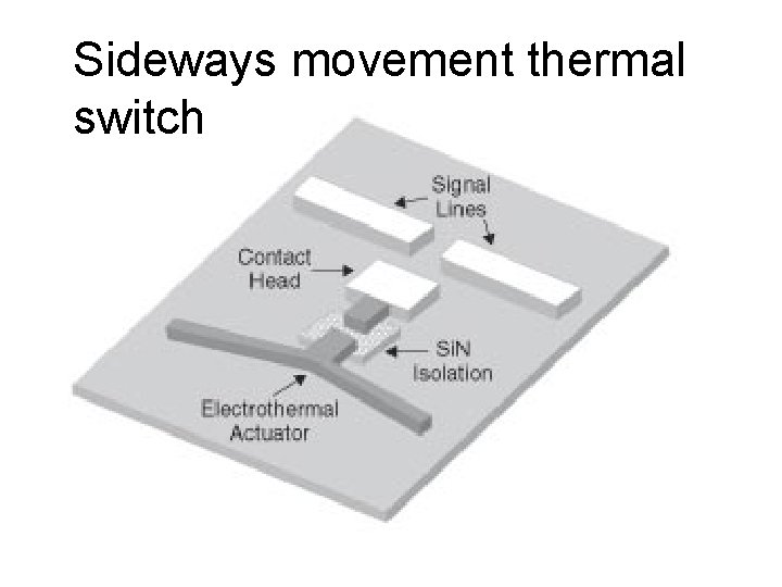
Sideways movement thermal switch

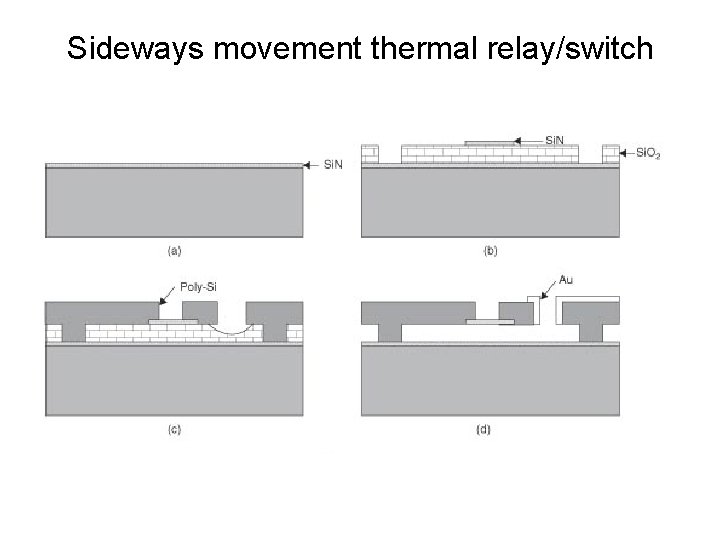
Sideways movement thermal relay/switch

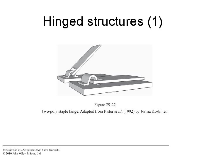
Hinged structures (1)

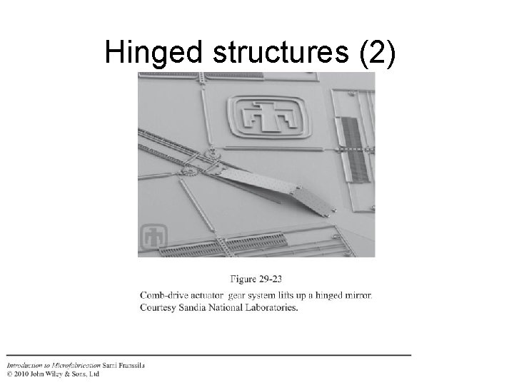
Hinged structures (2)

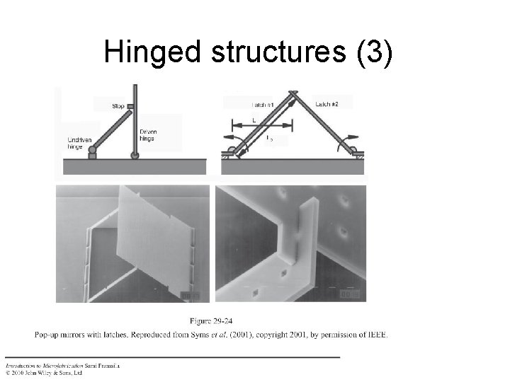
Hinged structures (3)

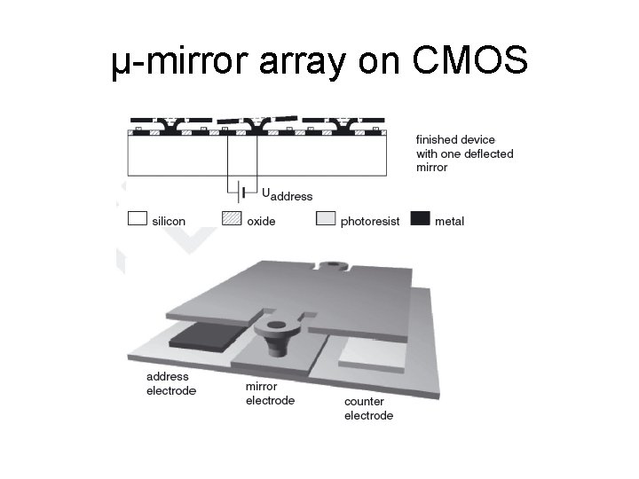
µ-mirror array on CMOS

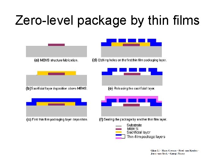
Zero-level package by thin films

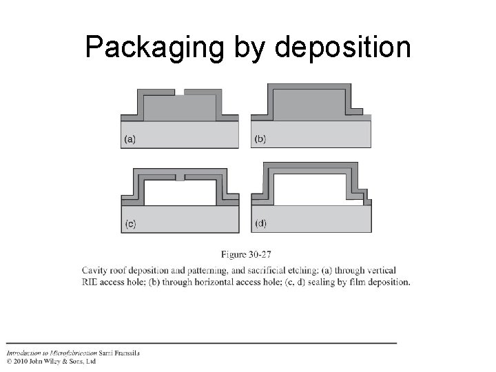
Packaging by deposition

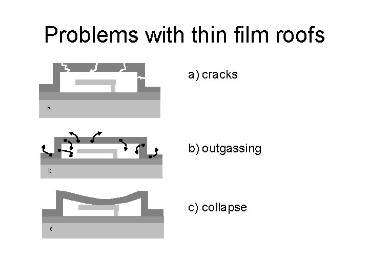
Problems with thin film roofs a) cracks a b) outgassing b c) collapse c

Bulk vs. surface • in bulk micromechanics <Si> is etched by either KOH or DRIE • structure heights 380 µm/500 µm • in surface micromechanics thin films (oxide, nitride, poly, aluminum) are used • structure heights 1 -2 µm typically (=sputter & CVD film thicknesses) or 5 -50 µm if SOI or thick poly used