MEMS 1 Bulk and SOIMEMS Chapters 29 30
 (Chapters 29 & 30) sami. franssila@aalto. fi")
MEMS 1 (Bulk and SOI-MEMS) (Chapters 29 & 30) sami. franssila@aalto. fi

Aspects of MEMS integration Highly 3 D Often double sided DRIE vs. KOH etching Bonding often involved Wafer 1 Wafer 2

Bulk micromechanics Wafer properties important, KOH etching 54. 7 o walls SOI micromechanics DRIE for patterning, isotropic oxide etching for release Surface micromechanics Deposition of 2 µm thick layers, RIE of structural layer, isotropic etching of sacrificial layer

Bulk MEMS, wet etching

Bulk MEMS, DRIE a b c Deng, W. et al: Increase of electrospray throughput using multiplexed microfabricated sources for the scalable generation of monodisperse droplets, J. Aerosol Sci. 37 (2006) pp. 696– 714

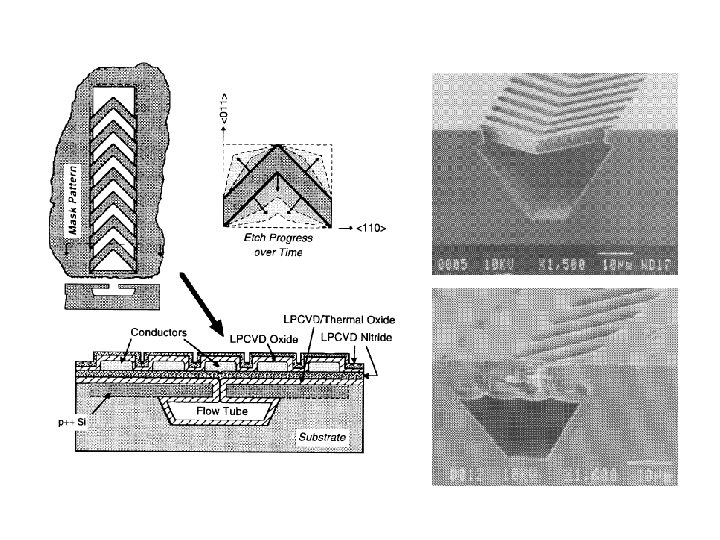
SOI MEMS

Surface MEMS "Physics and Technology of Silicon Carbide Devices", book edited by Yasuto Hijikata, http: //phys. org/news/2010 -12 -panasonicimec-thin-packaged-mems. html
 Some alignments")
Double side alignment Double sided lithography requires DSP wafers (Double Side Polished) Some alignments are critical but not all ! Often the backside structures are large, and not critically aligned to top side features.

Alignment: diffused piezoresistors Piezoresistors have to be positioned at the maximum defelection region OK NOT OK

Bulk MEMS, wet etching

Membrane formation Nitride membrane; no timing needed Timed silicon membrane; thickness depends on etch rate and wafer thickness control. Thin membrane thickness control bad. SOI wafer, membrane thickness determined by SOI device layer thickness

Micro hot plate fabrication steps sensor material Pt measurement electrodes oxide Nitride Pt heater 0. Double side polished <100> wafer 1. CVD nitride on both sides 2. Litho on backside for nitride 3. Nitride RIE & resist strip 4. On front: Pt heater sputter 5. Litho of Pt heater 6. Pt etch & strip 7. CVD oxide 8. Pt measurement electrode sputter 9. Litho of Pt measurement electrodes 10. Pt etch & resist strip 11. Litho to reveal Pt heater for wire bond 12. Oxide etch & strip 13. Frontside protection (jig) 14. Backside KOH etch 15. Sensor material depo & patterning

Single sided KOH etching jig http: //www. ammt. com/products/wet-etching/single-series/

Jigs

Thermal pressure sensor

Thermal pressure sensor heat sink heater resistor p 1 p 0 thermopile nitride

Cantilever flowsensor:

Convex corner undercutting From: Maluf

Undercut by misorientation

Membrane structures by top side micromachining

Polarization-selective uncooled infrared sensor with asymmetric twodimensional plasmonic absorber Shinpei Ogawa ; Kyohei Masuda ; Yousuke Takagawa ; Masafumi Kimata [+] Author Affiliations Opt. Eng. 53(10), 107110

Ink jet
 Process flow for ink jet: Thermal oxidation, 1 µm thick Litho")
Ink jet (2) Process flow for ink jet: Thermal oxidation, 1 µm thick Litho #1: chip area definition Oxide etching Boron diffusion, 2 µm deep Litho #2: chevron pattern: 1 µm width RIE of silicon, 4 µm deep Anisotropic silicon etching to undercut p++ chevrons Thermal oxidation LPCVD nitride deposition for chevron roof sealing Etchback (or polishing) of nitride LPCVD polysilicon deposition Poly doping, 20 Ohm/sq

 Litho #3: poly heater pattern Polysilicon etching Aluminum sputtering Litho #4:")
Ink jet (4) Litho #3: poly heater pattern Polysilicon etching Aluminum sputtering Litho #4: metal pads Aluminum etching Passivation: CVD oxide 1 µm + PECVD nitride 0. 3 µm Lithography #5: opening of bonding pads RIE of nitride and oxide Lithography #6: pattern for gold lift-off Evaporation of Cr/Au Lift of Cr/Au Lithography #7: fluidic inlet definition on the backside Anisotropic etching through the wafer from the back Resist stripping and cleaning steps omitted

Single mask SOI accelerometer 1. Device silicon layer DRIE 2. Buried oxide HF wet etch 3. Rinse & dry Benefit of SOI: Single crystal silicon, good mechanical properties Buried layer readymade

Cavity-SOI oxide Al electrode Si membrane air cavity ground electrode Most the 2 nd wafer etched away Remaining Si of 2 nd wafer Bulk Si wafer

Cavity-SOI fabrication oxide Al electrode Si membrane air cavity ground electrode 1. Silicon bulk wafer 2. Lithography of air cavity 3. DRIE of silicon & strip PR 4. Cleaning 5. Thermal oxidation 6. Bonding with a 2 nd wafer 7. Thinning by KOH etching 8. Al electrode sputtering 9. Litho & Al etch & strip 10. CVD oxide

C-SOI: No need for release etching. Additional benefit of SOI: Single crystal silicon with superior mechanical properties, e. g. low stress

Bonded microphone Membrane chip with Au/Sn solder bumbs air gap acoustic holes Backplate chip with acoustic holes Franssila: Introduction to Microfabrication

IR spectrometer

CMOS-MEMS-bulk integration
 b) c) d) DRIE and")
CMOS-MEMS-SOI a c b d Dougherty, JMEMS 2003 a) b) c) d) DRIE and semipermeable polysilicon deposition; buried oxide etching through semi-permeable poly deposition of standard polysilicon and CMP IC processing and release hole etching by DRIE

Summary Wafer selection: • <100> SSP wafers ? • <100> DSP wafers ? • SOI wafers ? Materials compatibility: • How high temperature does glass wafer tolerate ? • Can cavity-SOI really be processed like standard wafer ? • What are the limitations of piezoelectric materials ? Process-device interactions: • Can thermal diffusion be used or is I/I preferred ? • Is DRIE etch profile ciritical or non-critical • Will the wafers bend due to thin film stresses ? Equipment and process capability: • How can we clean wafers with released structures ? • How thick roof can we deposit ? • Can thick bonded wafer stacks be inserted to wafer boats ?
 Design rules: • What is the smallest allowed linewidth on front side")
Summary (2) Design rules: • What is the smallest allowed linewidth on front side ? • What is the minimum linewidth for backside thru-wafer DRIE ? • What is front-to-back alignment accuracy ? Mask considerations: • Which photomasks are critical, which are non-critical ? • Does etch undercutting need to be compensated on the mask ? Order of process steps: • Should front side processing be completed before backside processing ? • Can any steps be done after thin membrane formation ? • Can any steps be done after thru-wafer holes have been made ? Reliability: • How do stresses build up when more layers are deposited ? • What vacuum does the resonator cavity need ? • What leak rate is allowed in the resonator cavity ?
- Slides: 36