Review Fig 4 15 page 320 Fig 4

![STATE S 0 S 1 S 2 S 3 S 4 Register Transfers M[PC] STATE S 0 S 1 S 2 S 3 S 4 Register Transfers M[PC]](https://slidetodoc.com/presentation_image_h2/a38f659c7342d4211a1744b53c4b840c/image-10.jpg)
![lw rt, imm 16 (rs) # load word M[ R[rs] + sign_ext(imm 16) ] lw rt, imm 16 (rs) # load word M[ R[rs] + sign_ext(imm 16) ]](https://slidetodoc.com/presentation_image_h2/a38f659c7342d4211a1744b53c4b840c/image-15.jpg)

![lw rt, imm 16 (rs) # load word M[ R[rs] + sign_ext(imm 16) ] lw rt, imm 16 (rs) # load word M[ R[rs] + sign_ext(imm 16) ]](https://slidetodoc.com/presentation_image_h2/a38f659c7342d4211a1744b53c4b840c/image-17.jpg)

![lw rt, imm 16 (rs) # load word M[ R[rs] + sign_ext(imm 16) ] lw rt, imm 16 (rs) # load word M[ R[rs] + sign_ext(imm 16) ]](https://slidetodoc.com/presentation_image_h2/a38f659c7342d4211a1744b53c4b840c/image-19.jpg)
![lw rt, imm 16 (rs) # load word M[ R[rs] + sign_ext(imm 16) ] lw rt, imm 16 (rs) # load word M[ R[rs] + sign_ext(imm 16) ]](https://slidetodoc.com/presentation_image_h2/a38f659c7342d4211a1744b53c4b840c/image-20.jpg)
![lw rt, imm 16 (rs) # load word M[ R[rs] + sign_ext(imm 16) ] lw rt, imm 16 (rs) # load word M[ R[rs] + sign_ext(imm 16) ]](https://slidetodoc.com/presentation_image_h2/a38f659c7342d4211a1744b53c4b840c/image-21.jpg)
![lw rt, imm 16 (rs) # load word M[ R[rs] + sign_ext(imm 16) ] lw rt, imm 16 (rs) # load word M[ R[rs] + sign_ext(imm 16) ]](https://slidetodoc.com/presentation_image_h2/a38f659c7342d4211a1744b53c4b840c/image-22.jpg)
![lw rt, imm 16 (rs) # load word M[ R[rs] + sign_ext(imm 16) ] lw rt, imm 16 (rs) # load word M[ R[rs] + sign_ext(imm 16) ]](https://slidetodoc.com/presentation_image_h2/a38f659c7342d4211a1744b53c4b840c/image-23.jpg)
![sw rt, imm 16 ( rs) # store word R[rt] M[ R[rs] + sign_ext(imm sw rt, imm 16 ( rs) # store word R[rt] M[ R[rs] + sign_ext(imm](https://slidetodoc.com/presentation_image_h2/a38f659c7342d4211a1744b53c4b840c/image-24.jpg)
![sw rt, imm 16 ( rs) # store word R[rt] M[ R[rs] + sign_ext(imm sw rt, imm 16 ( rs) # store word R[rt] M[ R[rs] + sign_ext(imm](https://slidetodoc.com/presentation_image_h2/a38f659c7342d4211a1744b53c4b840c/image-25.jpg)

![R – Arithmetic – Logic Instruction op rd, rs, rt R[rs] op R[rt] R R – Arithmetic – Logic Instruction op rd, rs, rt R[rs] op R[rt] R](https://slidetodoc.com/presentation_image_h2/a38f659c7342d4211a1744b53c4b840c/image-27.jpg)
![R – Arithmetic – Logic Instruction op rd, rs, rt R[rs] op R[rt] R R – Arithmetic – Logic Instruction op rd, rs, rt R[rs] op R[rt] R](https://slidetodoc.com/presentation_image_h2/a38f659c7342d4211a1744b53c4b840c/image-28.jpg)
![R – Arithmetic – Logic Instruction op rd, rs, rt R[rs] op R[rt] R R – Arithmetic – Logic Instruction op rd, rs, rt R[rs] op R[rt] R](https://slidetodoc.com/presentation_image_h2/a38f659c7342d4211a1744b53c4b840c/image-29.jpg)
![R – Arithmetic – Logic Instruction op rd, rs, rt R[rs] op R[rt] R R – Arithmetic – Logic Instruction op rd, rs, rt R[rs] op R[rt] R](https://slidetodoc.com/presentation_image_h2/a38f659c7342d4211a1744b53c4b840c/image-30.jpg)
![R – Arithmetic – Logic Instruction op rd, rs, rt R[rs] op R[rt] R R – Arithmetic – Logic Instruction op rd, rs, rt R[rs] op R[rt] R](https://slidetodoc.com/presentation_image_h2/a38f659c7342d4211a1744b53c4b840c/image-31.jpg)



![State Register Transfers S 0 M[PC] IR, PC + 4 PC, S 1 S State Register Transfers S 0 M[PC] IR, PC + 4 PC, S 1 S](https://slidetodoc.com/presentation_image_h2/a38f659c7342d4211a1744b53c4b840c/image-43.jpg)
![State Register Transfers S 0 M[PC] IR, PC + 4 PC, S 1 R[IR[25 State Register Transfers S 0 M[PC] IR, PC + 4 PC, S 1 R[IR[25](https://slidetodoc.com/presentation_image_h2/a38f659c7342d4211a1744b53c4b840c/image-44.jpg)

![State Register Transfers S 0 M[PC] IR, PC + 4 PC, S 1 R[IR[25 State Register Transfers S 0 M[PC] IR, PC + 4 PC, S 1 R[IR[25](https://slidetodoc.com/presentation_image_h2/a38f659c7342d4211a1744b53c4b840c/image-46.jpg)
![State Register Transfers S 0 M[PC] IR, PC + 4 PC, S 1 R[IR[25 State Register Transfers S 0 M[PC] IR, PC + 4 PC, S 1 R[IR[25](https://slidetodoc.com/presentation_image_h2/a38f659c7342d4211a1744b53c4b840c/image-47.jpg)
![State Register Transfers S 0 M[PC] IR, PC + 4 PC, S 1 R[IR[25 State Register Transfers S 0 M[PC] IR, PC + 4 PC, S 1 R[IR[25](https://slidetodoc.com/presentation_image_h2/a38f659c7342d4211a1744b53c4b840c/image-48.jpg)
![State Register Transfers S 0 M[PC] IR, PC + 4 PC, S 1 R[IR[25 State Register Transfers S 0 M[PC] IR, PC + 4 PC, S 1 R[IR[25](https://slidetodoc.com/presentation_image_h2/a38f659c7342d4211a1744b53c4b840c/image-49.jpg)
![R – Arithmetic – Logic Instruction op rd, rs, rt R[rs] op R[rt] R R – Arithmetic – Logic Instruction op rd, rs, rt R[rs] op R[rt] R](https://slidetodoc.com/presentation_image_h2/a38f659c7342d4211a1744b53c4b840c/image-50.jpg)
![State Register Transfers S 0 M[PC] IR, PC + 4 PC, S 1 R[IR[25 State Register Transfers S 0 M[PC] IR, PC + 4 PC, S 1 R[IR[25](https://slidetodoc.com/presentation_image_h2/a38f659c7342d4211a1744b53c4b840c/image-51.jpg)
![State Register Transfers S 0 M[PC] IR, PC + 4 PC, S 1 R[IR[25 State Register Transfers S 0 M[PC] IR, PC + 4 PC, S 1 R[IR[25](https://slidetodoc.com/presentation_image_h2/a38f659c7342d4211a1744b53c4b840c/image-52.jpg)

![State Register Transfers S 0 M[PC] IR, PC + 4 PC, S 1 R[IR[25 State Register Transfers S 0 M[PC] IR, PC + 4 PC, S 1 R[IR[25](https://slidetodoc.com/presentation_image_h2/a38f659c7342d4211a1744b53c4b840c/image-54.jpg)
![State Register Transfers S 0 M[PC] IR, PC + 4 PC, S 1 R[IR[25 State Register Transfers S 0 M[PC] IR, PC + 4 PC, S 1 R[IR[25](https://slidetodoc.com/presentation_image_h2/a38f659c7342d4211a1744b53c4b840c/image-56.jpg)
![What would “Halt” look like? S 0 S 10 M[PC] IR, PC + 4 What would “Halt” look like? S 0 S 10 M[PC] IR, PC + 4](https://slidetodoc.com/presentation_image_h2/a38f659c7342d4211a1744b53c4b840c/image-57.jpg)
![What would “Halt” look like? S 0 S 1 M[PC] IR, PC + 4 What would “Halt” look like? S 0 S 1 M[PC] IR, PC + 4](https://slidetodoc.com/presentation_image_h2/a38f659c7342d4211a1744b53c4b840c/image-58.jpg)
![What if a Memory Read took 3 clock cycles? Instead of S 0 M[PC] What if a Memory Read took 3 clock cycles? Instead of S 0 M[PC]](https://slidetodoc.com/presentation_image_h2/a38f659c7342d4211a1744b53c4b840c/image-60.jpg)
- Slides: 60


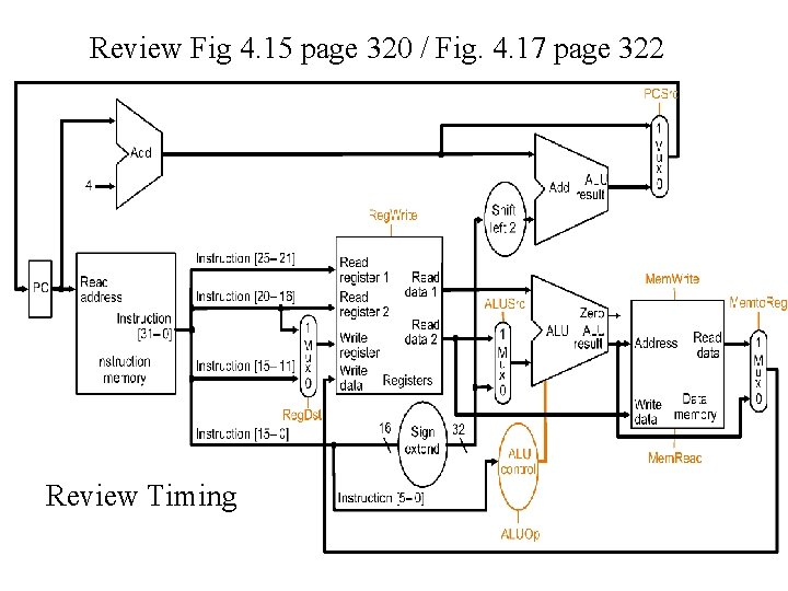
Review Fig 4. 15 page 320 / Fig. 4. 17 page 322 Review Timing

Multicycle Implementation • Realistic Approach • Enables time sharing functional units during an instruction ( Memory and ALU) • Enables instructions to be implemented with different number of clock cycles

Multicycle Implementation Assumptions: • Each STEP in the execution will take 1 clock cycle

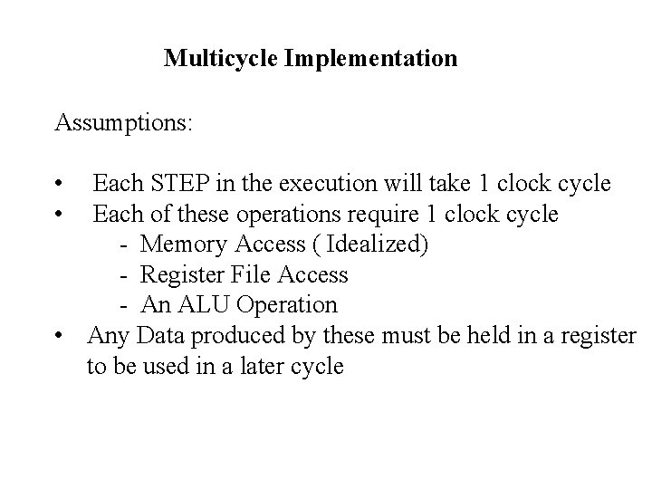
Multicycle Implementation Assumptions: • • Each STEP in the execution will take 1 clock cycle Each of these operations require 1 clock cycle - Memory Access ( Idealized) - Register File Access - An ALU Operation

Multicycle Implementation Assumptions: • • Each STEP in the execution will take 1 clock cycle Each of these operations require 1 clock cycle - Memory Access ( Idealized) - Register File Access - An ALU Operation • Any Data produced by these must be held in a register to be used in a later cycle

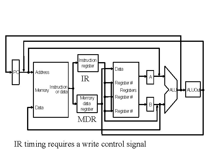
Instruction register PC Address Memory Data IR Instruction or data Memory data register Data A Register # ALU Registers Register # B Register # MDR IR timing requires a write control signal ALUOut

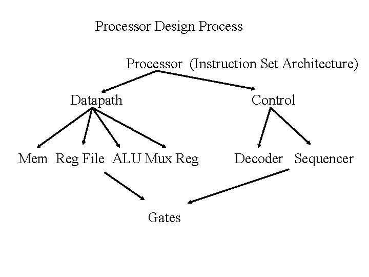
Processor Design Processor (Instruction Set Architecture) Datapath Control Mem Reg File ALU Mux Reg Gates Decoder Sequencer

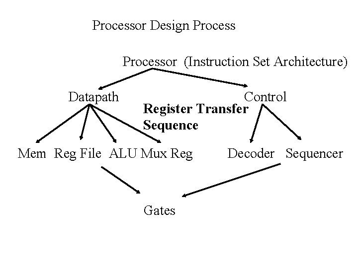
Processor Design Processor (Instruction Set Architecture) Datapath Control Register Transfer Sequence Mem Reg File ALU Mux Reg Gates Decoder Sequencer
![STATE S 0 S 1 S 2 S 3 S 4 Register Transfers MPC STATE S 0 S 1 S 2 S 3 S 4 Register Transfers M[PC]](https://slidetodoc.com/presentation_image_h2/a38f659c7342d4211a1744b53c4b840c/image-10.jpg)
STATE S 0 S 1 S 2 S 3 S 4 Register Transfers M[PC] IR, PC+4 PC, R[IR[25 -21]] A, A + sign_ext(IR[15 -0]) ALUOut, M[ ALUOut] MDR, MDR R[ IR[20 -16]], NEXT STATE S 1 S 2 S 3 S 4 S 0 S S S

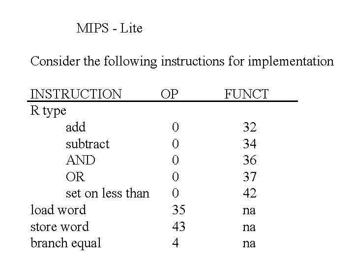
MIPS - Lite Consider the following instructions for implementation INSTRUCTION OP R type add 0 subtract 0 AND 0 OR 0 set on less than 0 load word 35 store word 43 branch equal 4 FUNCT 32 34 36 37 42 na na na

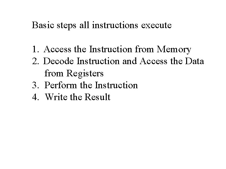
Basic steps all instructions execute 1. Access the Instruction from Memory 2. Decode Instruction and Access the Data from Registers 3. Perform the Instruction 4. Write the Result

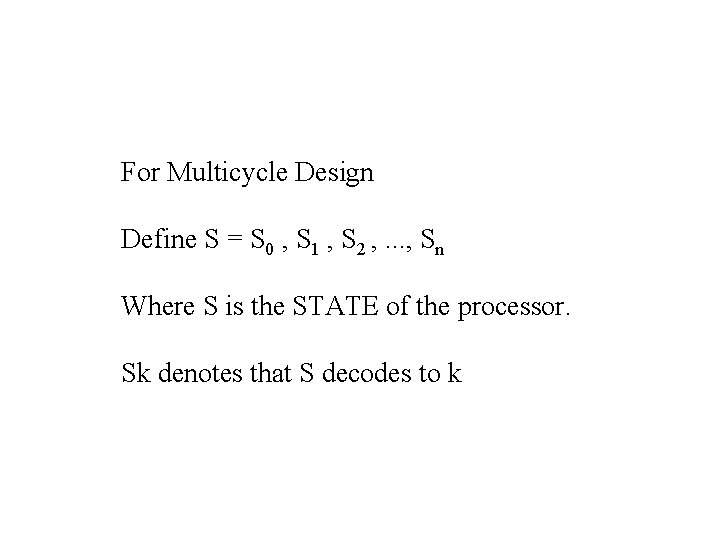
For Multicycle Design Define S = S 0 , S 1 , S 2 , . . . , Sn Where S is the STATE of the processor. Sk denotes that S decodes to k

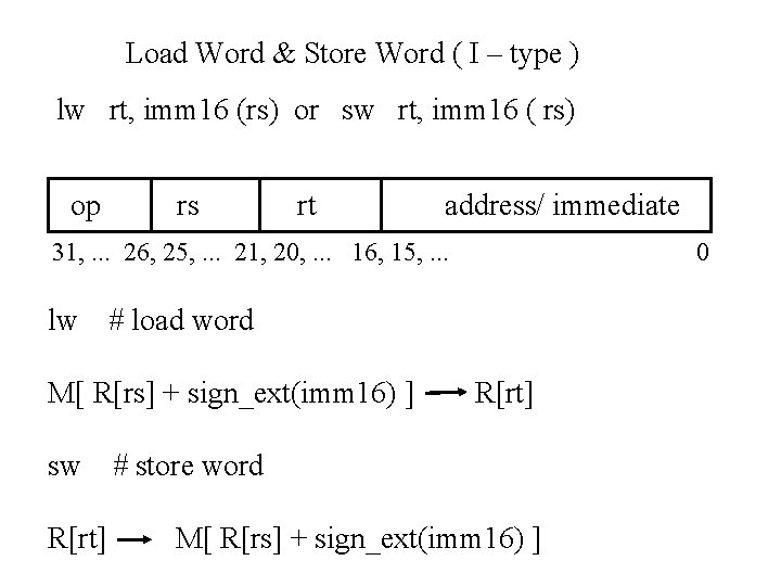
Load Word & Store Word ( I – type ) lw rt, imm 16 (rs) or sw rt, imm 16 ( rs) op rs rt address/ immediate 31, . . . 26, 25, . . . 21, 20, . . . 16, 15, . . . lw # load word M[ R[rs] + sign_ext(imm 16) ] sw R[rt] 0 R[rt] # store word M[ R[rs] + sign_ext(imm 16) ]
![lw rt imm 16 rs load word M Rrs signextimm 16 lw rt, imm 16 (rs) # load word M[ R[rs] + sign_ext(imm 16) ]](https://slidetodoc.com/presentation_image_h2/a38f659c7342d4211a1744b53c4b840c/image-15.jpg)
lw rt, imm 16 (rs) # load word M[ R[rs] + sign_ext(imm 16) ] R[rt] For Op = ‘LW’ S 0 M[PC] IR, PC+4 PC, Next State S 1 S

Instruction register PC Address Memory Data IR Instruction or data Memory data register Data A Register # ALU Registers Register # B Register # MDR IR timing requires a write control signal ALUOut
![lw rt imm 16 rs load word M Rrs signextimm 16 lw rt, imm 16 (rs) # load word M[ R[rs] + sign_ext(imm 16) ]](https://slidetodoc.com/presentation_image_h2/a38f659c7342d4211a1744b53c4b840c/image-17.jpg)
lw rt, imm 16 (rs) # load word M[ R[rs] + sign_ext(imm 16) ] R[rt] For Op = ‘LW’ S 0 M[PC] IR, PC+4 S 1 R[IR[25 -21]] A, PC, S 1 S 2 S S

Instruction register PC Address Memory Data IR Instruction or data Memory data register Data A Register # ALU Registers Register # B Register # MDR IR timing requires a write control signal ALUOut
![lw rt imm 16 rs load word M Rrs signextimm 16 lw rt, imm 16 (rs) # load word M[ R[rs] + sign_ext(imm 16) ]](https://slidetodoc.com/presentation_image_h2/a38f659c7342d4211a1744b53c4b840c/image-19.jpg)
lw rt, imm 16 (rs) # load word M[ R[rs] + sign_ext(imm 16) ] R[rt] For Op = ‘LW’ S 0 M[PC] IR, PC+4 PC, S 1 R[IR[25 -21]] A, S 2 A + sign_ext(IR[15 -0]) ALUOut, S 1 S S 2 S S 3 S
![lw rt imm 16 rs load word M Rrs signextimm 16 lw rt, imm 16 (rs) # load word M[ R[rs] + sign_ext(imm 16) ]](https://slidetodoc.com/presentation_image_h2/a38f659c7342d4211a1744b53c4b840c/image-20.jpg)
lw rt, imm 16 (rs) # load word M[ R[rs] + sign_ext(imm 16) ] R[rt] For Op = ‘LW’ S 0 M[PC] IR, PC+4 PC, S 1 R[IR[25 -21]] A, S 2 A + sign_ext(IR[15 -0]) ALUOut, S 3 M[ ALUOut] MDR, S 1 S S 2 S S 3 S S 4 S
![lw rt imm 16 rs load word M Rrs signextimm 16 lw rt, imm 16 (rs) # load word M[ R[rs] + sign_ext(imm 16) ]](https://slidetodoc.com/presentation_image_h2/a38f659c7342d4211a1744b53c4b840c/image-21.jpg)
lw rt, imm 16 (rs) # load word M[ R[rs] + sign_ext(imm 16) ] R[rt] For Op = ‘LW’ S 0 M[PC] IR, PC+4 PC, S 1 R[IR[25 -21]] A, S 2 A + sign_ext(IR[15 -0]) ALUOut, S 3 M[ ALUOut] MDR, S 4 MDR R[ IR[20 -16]], S 1 S 2 S 3 S 4 S 0 S S S
![lw rt imm 16 rs load word M Rrs signextimm 16 lw rt, imm 16 (rs) # load word M[ R[rs] + sign_ext(imm 16) ]](https://slidetodoc.com/presentation_image_h2/a38f659c7342d4211a1744b53c4b840c/image-22.jpg)
lw rt, imm 16 (rs) # load word M[ R[rs] + sign_ext(imm 16) ] R[rt] For Op = ‘LW’ S 0 M[PC] IR, PC+4 PC, S 1 R[IR[25 -21]] A, S 2 A + sign_ext(IR[15 -0]) ALUOut, S 3 M[ ALUOut] MDR, S 4 MDR R[ IR[20 -16]], sw rt, imm 16 ( rs) R[rt] # store word M[ R[rs] + sign_ext(imm 16) ] What’s different? S 1 S 2 S 3 S 4 S 0 S S S
![lw rt imm 16 rs load word M Rrs signextimm 16 lw rt, imm 16 (rs) # load word M[ R[rs] + sign_ext(imm 16) ]](https://slidetodoc.com/presentation_image_h2/a38f659c7342d4211a1744b53c4b840c/image-23.jpg)
lw rt, imm 16 (rs) # load word M[ R[rs] + sign_ext(imm 16) ] R[rt] For Op = ‘LW’ S 0 M[PC] IR, PC+4 PC, S 1 R[IR[25 -21]] A, R[IR[20 -16]] B S 2 A + sign_ext(IR[15 -0]) ALUOut, S 3 M[ ALUOut] MDR, S 4 MDR R[ IR[20 -16]], sw rt, imm 16 ( rs) R[rt] # store word M[ R[rs] + sign_ext(imm 16) ] What’s different? S 1 S S 2 S 3 S S 4 S S 0 S
![sw rt imm 16 rs store word Rrt M Rrs signextimm sw rt, imm 16 ( rs) # store word R[rt] M[ R[rs] + sign_ext(imm](https://slidetodoc.com/presentation_image_h2/a38f659c7342d4211a1744b53c4b840c/image-24.jpg)
sw rt, imm 16 ( rs) # store word R[rt] M[ R[rs] + sign_ext(imm 16) ] For Op = ‘SW’ S 0 M[PC] IR, PC+4 PC, S 1 R[IR[25 -21]] A, R[IR[20 -16]] B S 2 A + sign_ext(IR[15 -0]) ALUOut, S 1 S S 2 S ? S
![sw rt imm 16 rs store word Rrt M Rrs signextimm sw rt, imm 16 ( rs) # store word R[rt] M[ R[rs] + sign_ext(imm](https://slidetodoc.com/presentation_image_h2/a38f659c7342d4211a1744b53c4b840c/image-25.jpg)
sw rt, imm 16 ( rs) # store word R[rt] M[ R[rs] + sign_ext(imm 16) ] For Op = ‘SW’ S 0 M[PC] IR, PC+4 PC, S 1 R[IR[25 -21]] A, R[IR[20 -16]] B S 2 A + sign_ext(IR[15 -0]) ALUOut, S 5 B M[ ALUOut], S 1 S 2 S 5 S S 0

Instruction register PC Address Memory Data IR Instruction or data Memory data register Data A Register # ALU Registers Register # B Register # MDR IR timing requires a write control signal ALUOut
![R Arithmetic Logic Instruction op rd rs rt Rrs op Rrt R R – Arithmetic – Logic Instruction op rd, rs, rt R[rs] op R[rt] R](https://slidetodoc.com/presentation_image_h2/a38f659c7342d4211a1744b53c4b840c/image-27.jpg)
R – Arithmetic – Logic Instruction op rd, rs, rt R[rs] op R[rt] R [rd] op rs rt rd 6 5 5 5 shamt funct 5 6
![R Arithmetic Logic Instruction op rd rs rt Rrs op Rrt R R – Arithmetic – Logic Instruction op rd, rs, rt R[rs] op R[rt] R](https://slidetodoc.com/presentation_image_h2/a38f659c7342d4211a1744b53c4b840c/image-28.jpg)
R – Arithmetic – Logic Instruction op rd, rs, rt R[rs] op R[rt] R [rd] Op = R-type S 0 M[PC] IR, PC + 4 PC, S 1 S
![R Arithmetic Logic Instruction op rd rs rt Rrs op Rrt R R – Arithmetic – Logic Instruction op rd, rs, rt R[rs] op R[rt] R](https://slidetodoc.com/presentation_image_h2/a38f659c7342d4211a1744b53c4b840c/image-29.jpg)
R – Arithmetic – Logic Instruction op rd, rs, rt R[rs] op R[rt] R [rd] Op = R-type S 0 S 1 M[PC] IR, PC + 4 PC, R[IR[25 -21]] A, R[IR[20 -16]] B, S 1 S 6 S S
![R Arithmetic Logic Instruction op rd rs rt Rrs op Rrt R R – Arithmetic – Logic Instruction op rd, rs, rt R[rs] op R[rt] R](https://slidetodoc.com/presentation_image_h2/a38f659c7342d4211a1744b53c4b840c/image-30.jpg)
R – Arithmetic – Logic Instruction op rd, rs, rt R[rs] op R[rt] R [rd] Op = R-type S 0 S 1 S 6 M[PC] IR, PC + 4 PC, R[IR[25 -21]] A, R[IR[20 -16]] A op B ALUOut, B, S 1 S 6 S 7 S S S
![R Arithmetic Logic Instruction op rd rs rt Rrs op Rrt R R – Arithmetic – Logic Instruction op rd, rs, rt R[rs] op R[rt] R](https://slidetodoc.com/presentation_image_h2/a38f659c7342d4211a1744b53c4b840c/image-31.jpg)
R – Arithmetic – Logic Instruction op rd, rs, rt R[rs] op R[rt] R [rd] Op = R-type S 0 S 1 S 6 S 7 M[PC] IR, PC + 4 PC, R[IR[25 -21]] A, R[IR[20 -16]] A op B ALUOut, ALUOut R[IR[15 -11]], B, S 1 S 6 S 7 S 0 S S

Instruction register PC Address Memory Data IR Instruction or data Memory data register Data A Register # ALU Registers Register # B Register # MDR IR timing requires a write control signal ALUOut

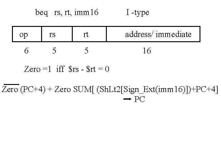
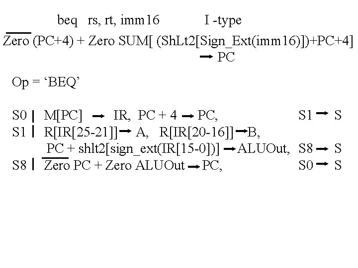
beq rs, rt, imm 16 op rs rt 6 5 5 I -type address/ immediate 16 Zero =1 iff $rs - $rt = 0 Zero (PC+4) + Zero SUM[ (Sh. Lt 2[Sign_Ext(imm 16)])+PC+4] PC

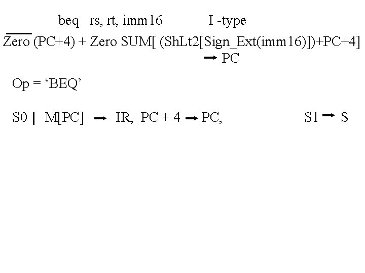
beq rs, rt, imm 16 I -type Zero (PC+4) + Zero SUM[ (Sh. Lt 2[Sign_Ext(imm 16)])+PC+4] PC Op = ‘BEQ’ S 0 M[PC] IR, PC + 4 PC, S 1 S

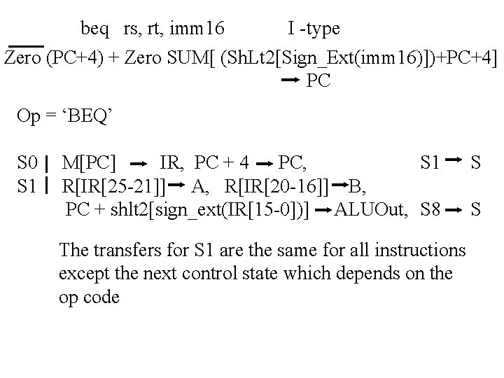
beq rs, rt, imm 16 I -type Zero (PC+4) + Zero SUM[ (Sh. Lt 2[Sign_Ext(imm 16)])+PC+4] PC Op = ‘BEQ’ S 0 S 1 M[PC] IR, PC + 4 PC, S 1 R[IR[25 -21]] A, R[IR[20 -16]] B, PC + shlt 2[sign_ext(IR[15 -0])] ALUOut, S 8 The transfers for S 1 are the same for all instructions except the next control state which depends on the op code S S

beq rs, rt, imm 16 I -type Zero (PC+4) + Zero SUM[ (Sh. Lt 2[Sign_Ext(imm 16)])+PC+4] PC Op = ‘BEQ’ S 0 S 1 S 8 M[PC] IR, PC + 4 PC, S 1 R[IR[25 -21]] A, R[IR[20 -16]] B, PC + shlt 2[sign_ext(IR[15 -0])] ALUOut, S 8 Zero PC + Zero ALUOut PC, S 0 S S S

Instruction register PC Address Memory Data IR Instruction or data Memory data register Data A Register # ALU Registers Register # B Register # MDR IR timing requires a write control signal ALUOut

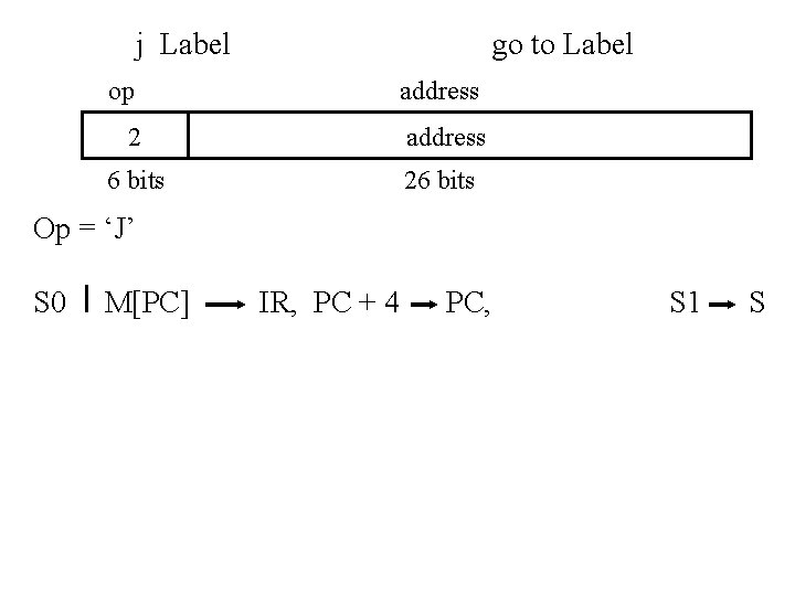
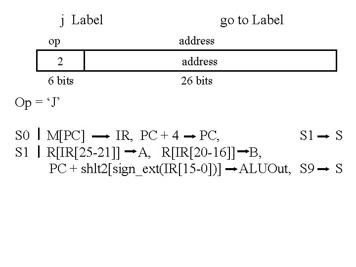
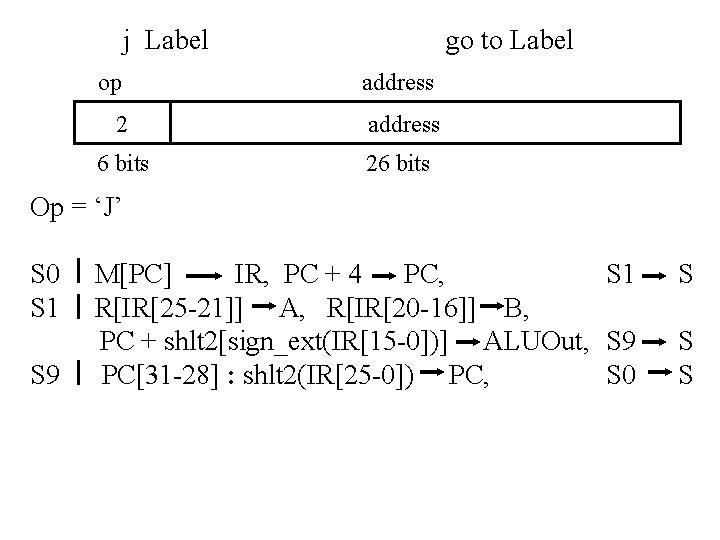
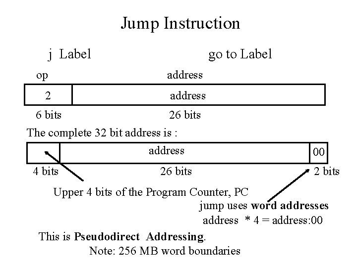
Jump Instruction j Label go to Label op address 2 address 6 bits 26 bits The complete 32 bit address is : address 4 bits 26 bits 00 2 bits Upper 4 bits of the Program Counter, PC jump uses word addresses address * 4 = address: 00 This is Pseudodirect Addressing. Note: 256 MB word boundaries

j Label go to Label op address 2 address 6 bits 26 bits Op = ‘J’ S 0 M[PC] IR, PC + 4 PC, S 1 S

j Label go to Label op address 2 address 6 bits 26 bits Op = ‘J’ S 0 S 1 M[PC] IR, PC + 4 PC, S 1 R[IR[25 -21]] A, R[IR[20 -16]] B, PC + shlt 2[sign_ext(IR[15 -0])] ALUOut, S 9 S S

j Label go to Label op address 2 address 6 bits 26 bits Op = ‘J’ S 0 S 1 S 9 M[PC] IR, PC + 4 PC, S 1 R[IR[25 -21]] A, R[IR[20 -16]] B, PC + shlt 2[sign_ext(IR[15 -0])] ALUOut, S 9 PC[31 -28] : shlt 2(IR[25 -0]) PC, S 0 S S S

Instruction register PC Address Memory Data IR Instruction or data Memory data register Data A Register # ALU Registers Register # B Register # MDR IR timing requires a write control signal ALUOut
![State Register Transfers S 0 MPC IR PC 4 PC S 1 S State Register Transfers S 0 M[PC] IR, PC + 4 PC, S 1 S](https://slidetodoc.com/presentation_image_h2/a38f659c7342d4211a1744b53c4b840c/image-43.jpg)
State Register Transfers S 0 M[PC] IR, PC + 4 PC, S 1 S
![State Register Transfers S 0 MPC IR PC 4 PC S 1 RIR25 State Register Transfers S 0 M[PC] IR, PC + 4 PC, S 1 R[IR[25](https://slidetodoc.com/presentation_image_h2/a38f659c7342d4211a1744b53c4b840c/image-44.jpg)
State Register Transfers S 0 M[PC] IR, PC + 4 PC, S 1 R[IR[25 -21]] A, R[IR[20 -16]] B, PC + shlt 2[sign_ext(IR[15 -0])] ALUOut, (‘LW’+’SW’)S 2 + ‘R’S 6 + ‘BEQ’S 8 + ‘J’S 9 S S

Load Word & Store Word ( I – type ) lw rt, imm 16 (rs) or sw rt, imm 16 ( rs) op rs rt address/ immediate 31, . . . 26, 25, . . . 21, 20, . . . 16, 15, . . . lw # load word M[ R[rs] + sign_ext(imm 16) ] sw R[rt] 0 R[rt] # store word M[ R[rs] + sign_ext(imm 16) ]
![State Register Transfers S 0 MPC IR PC 4 PC S 1 RIR25 State Register Transfers S 0 M[PC] IR, PC + 4 PC, S 1 R[IR[25](https://slidetodoc.com/presentation_image_h2/a38f659c7342d4211a1744b53c4b840c/image-46.jpg)
State Register Transfers S 0 M[PC] IR, PC + 4 PC, S 1 R[IR[25 -21]] A, R[IR[20 -16]] B, PC + shlt 2[sign_ext(IR[15 -0])] ALUOut, (‘LW’+’SW’)S 2 + ‘R’S 6 + ‘BEQ’S 8 + ‘J’S 9 S 2 A + sign_ext(IR[15 -0]) ALUOut, ‘LW’S 3 + ‘SW’S 5 S S S
![State Register Transfers S 0 MPC IR PC 4 PC S 1 RIR25 State Register Transfers S 0 M[PC] IR, PC + 4 PC, S 1 R[IR[25](https://slidetodoc.com/presentation_image_h2/a38f659c7342d4211a1744b53c4b840c/image-47.jpg)
State Register Transfers S 0 M[PC] IR, PC + 4 PC, S 1 R[IR[25 -21]] A, R[IR[20 -16]] B, PC + shlt 2[sign_ext(IR[15 -0])] ALUOut, (‘LW’+’SW’)S 2 + ‘R’S 6 + ‘BEQ’S 8 + ‘J’S 9 S 2 A + sign_ext(IR[15 -0]) ALUOut, ‘LW’S 3 + ‘SW’S 5 S 3 M[ ALUOut] MDR, S 4 S S
![State Register Transfers S 0 MPC IR PC 4 PC S 1 RIR25 State Register Transfers S 0 M[PC] IR, PC + 4 PC, S 1 R[IR[25](https://slidetodoc.com/presentation_image_h2/a38f659c7342d4211a1744b53c4b840c/image-48.jpg)
State Register Transfers S 0 M[PC] IR, PC + 4 PC, S 1 R[IR[25 -21]] A, R[IR[20 -16]] B, PC + shlt 2[sign_ext(IR[15 -0])] ALUOut, (‘LW’+’SW’)S 2 + ‘R’S 6 + ‘BEQ’S 8 + ‘J’S 9 S 2 A + sign_ext(IR[15 -0]) ALUOut, ‘LW’S 3 + ‘SW’S 5 S 3 M[ ALUOut] MDR, S 4 MDR R[ IR[20 -16]], S 0 S S S
![State Register Transfers S 0 MPC IR PC 4 PC S 1 RIR25 State Register Transfers S 0 M[PC] IR, PC + 4 PC, S 1 R[IR[25](https://slidetodoc.com/presentation_image_h2/a38f659c7342d4211a1744b53c4b840c/image-49.jpg)
State Register Transfers S 0 M[PC] IR, PC + 4 PC, S 1 R[IR[25 -21]] A, R[IR[20 -16]] B, PC + shlt 2[sign_ext(IR[15 -0])] ALUOut, (‘LW’+’SW’)S 2 + ‘R’S 6 + ‘BEQ’S 8 + ‘J’S 9 S 2 A + sign_ext(IR[15 -0]) ALUOut, ‘LW’S 3 + ‘SW’S 5 S 3 M[ ALUOut] MDR, S 4 MDR R[ IR[20 -16]], S 0 S 5 B M[ ALUOut], S S S 0
![R Arithmetic Logic Instruction op rd rs rt Rrs op Rrt R R – Arithmetic – Logic Instruction op rd, rs, rt R[rs] op R[rt] R](https://slidetodoc.com/presentation_image_h2/a38f659c7342d4211a1744b53c4b840c/image-50.jpg)
R – Arithmetic – Logic Instruction op rd, rs, rt R[rs] op R[rt] R [rd] op rs rt rd 6 5 5 5 shamt funct 5 6
![State Register Transfers S 0 MPC IR PC 4 PC S 1 RIR25 State Register Transfers S 0 M[PC] IR, PC + 4 PC, S 1 R[IR[25](https://slidetodoc.com/presentation_image_h2/a38f659c7342d4211a1744b53c4b840c/image-51.jpg)
State Register Transfers S 0 M[PC] IR, PC + 4 PC, S 1 R[IR[25 -21]] A, R[IR[20 -16]] B, PC + shlt 2[sign_ext(IR[15 -0])] ALUOut, (‘LW’+’SW’)S 2 + ‘R’S 6 + ‘BEQ’S 8 + ‘J’S 9 S 2 A + sign_ext(IR[15 -0]) ALUOut, ‘LW’S 3 + ‘SW’S 5 S 3 M[ ALUOut] MDR, S 4 MDR R[ IR[20 -16]], S 0 S 5 B M[ ALUOut], S 6 A op B ALUOut, S 7 S S S 0 S
![State Register Transfers S 0 MPC IR PC 4 PC S 1 RIR25 State Register Transfers S 0 M[PC] IR, PC + 4 PC, S 1 R[IR[25](https://slidetodoc.com/presentation_image_h2/a38f659c7342d4211a1744b53c4b840c/image-52.jpg)
State Register Transfers S 0 M[PC] IR, PC + 4 PC, S 1 R[IR[25 -21]] A, R[IR[20 -16]] B, PC + shlt 2[sign_ext(IR[15 -0])] ALUOut, (‘LW’+’SW’)S 2 + ‘R’S 6 + ‘BEQ’S 8 + ‘J’S 9 S 2 A + sign_ext(IR[15 -0]) ALUOut, ‘LW’S 3 + ‘SW’S 5 S 3 M[ ALUOut] MDR, S 4 MDR R[ IR[20 -16]], S 0 S 5 B M[ ALUOut], S 6 A op B ALUOut, S 7 ALUOut R[IR[15 -11]], S 0 S S

beq rs, rt, imm 16 op rs rt 6 5 5 I -type address/ immediate 16 Zero =1 iff $rs - $rt = 0 Zero (PC+4) + Zero SUM[ (Sh. Lt 2[Sign_Ext(imm 16)])+PC+4] PC
![State Register Transfers S 0 MPC IR PC 4 PC S 1 RIR25 State Register Transfers S 0 M[PC] IR, PC + 4 PC, S 1 R[IR[25](https://slidetodoc.com/presentation_image_h2/a38f659c7342d4211a1744b53c4b840c/image-54.jpg)
State Register Transfers S 0 M[PC] IR, PC + 4 PC, S 1 R[IR[25 -21]] A, R[IR[20 -16]] B, PC + shlt 2[sign_ext(IR[15 -0])] ALUOut, (‘LW’+’SW’)S 2 + ‘R’S 6 + ‘BEQ’S 8 + ‘J’S 9 S 2 A + sign_ext(IR[15 -0]) ALUOut, ‘LW’S 3 + ‘SW’S 5 S 3 M[ ALUOut] MDR, S 4 MDR R[ IR[20 -16]], S 0 S 5 B M[ ALUOut], S 6 A op B ALUOut, S 7 ALUOut R[IR[15 -11]], S 0 S 8 Zero PC + Zero ALUOut PC, S 0 S S S

Jump Instruction j Label go to Label op address 2 address 6 bits 26 bits The complete 32 bit address is : address 4 bits 26 bits 00 2 bits Upper 4 bits of the Program Counter, PC jump uses word addresses address * 4 = address: 00 This is Pseudodirect Addressing. Note: 256 MB word boundaries
![State Register Transfers S 0 MPC IR PC 4 PC S 1 RIR25 State Register Transfers S 0 M[PC] IR, PC + 4 PC, S 1 R[IR[25](https://slidetodoc.com/presentation_image_h2/a38f659c7342d4211a1744b53c4b840c/image-56.jpg)
State Register Transfers S 0 M[PC] IR, PC + 4 PC, S 1 R[IR[25 -21]] A, R[IR[20 -16]] B, PC + shlt 2[sign_ext(IR[15 -0])] ALUOut, (‘LW’+’SW’)S 2 + ‘R’S 6 + ‘BEQ’S 8 + ‘J’S 9 S 2 A + sign_ext(IR[15 -0]) ALUOut, ‘LW’S 3 + ‘SW’S 5 S 3 M[ ALUOut] MDR, S 4 MDR R[ IR[20 -16]], S 0 S 5 B M[ ALUOut], S 6 A op B ALUOut, S 7 ALUOut R[IR[15 -11]], S 0 S 8 Zero PC + Zero ALUOut PC, S 0 S 9 PC[31 -28] : shlt 2(IR[25 -0]) PC, S 0 S S
![What would Halt look like S 0 S 10 MPC IR PC 4 What would “Halt” look like? S 0 S 10 M[PC] IR, PC + 4](https://slidetodoc.com/presentation_image_h2/a38f659c7342d4211a1744b53c4b840c/image-57.jpg)
What would “Halt” look like? S 0 S 10 M[PC] IR, PC + 4 PC, S 1 R[IR[25 -21]] A, R[IR[20 -16]] B, PC + shlt 2[sign_ext(IR[15 -0])] ALUOut, (‘LW’+’SW’)S 2 + ‘R’S 6 + ‘BEQ’S 8 + ‘J’S 9 + ‘Halt’ S 10 S S
![What would Halt look like S 0 S 1 MPC IR PC 4 What would “Halt” look like? S 0 S 1 M[PC] IR, PC + 4](https://slidetodoc.com/presentation_image_h2/a38f659c7342d4211a1744b53c4b840c/image-58.jpg)
What would “Halt” look like? S 0 S 1 M[PC] IR, PC + 4 PC, S 1 R[IR[25 -21]] A, R[IR[20 -16]] B, PC + shlt 2[sign_ext(IR[15 -0])] ALUOut, (‘LW’+’SW’)S 2 + ‘R’S 6 + ‘BEQ’S 8 + ‘J’S 9 + ‘Halt’ S 10 S S S

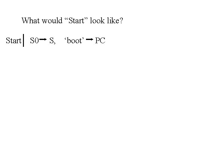
What would “Start” look like? Start S 0 S, ‘boot’ PC
![What if a Memory Read took 3 clock cycles Instead of S 0 MPC What if a Memory Read took 3 clock cycles? Instead of S 0 M[PC]](https://slidetodoc.com/presentation_image_h2/a38f659c7342d4211a1744b53c4b840c/image-60.jpg)
What if a Memory Read took 3 clock cycles? Instead of S 0 M[PC] It would be S 0 M[PC] S 1 S 2 IR, PC + 4 PC, S 1 S PC S 1 S 2 S 3 S S S IR PC + 4