Lecture Presentation Chapter 12 Solids and Modern Materials
- Slides: 46

Lecture Presentation Chapter 12 Solids and Modern Materials © 2012 Pearson Education, Inc. John D. Bookstaver St. Charles Community College Cottleville, MO

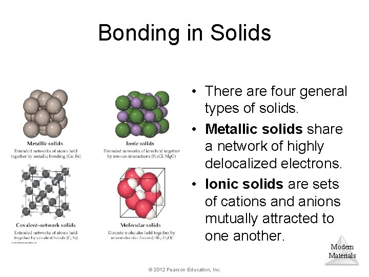
Bonding in Solids • There are four general types of solids. • Metallic solids share a network of highly delocalized electrons. • Ionic solids are sets of cations and anions mutually attracted to one another. Modern Materials © 2012 Pearson Education, Inc.

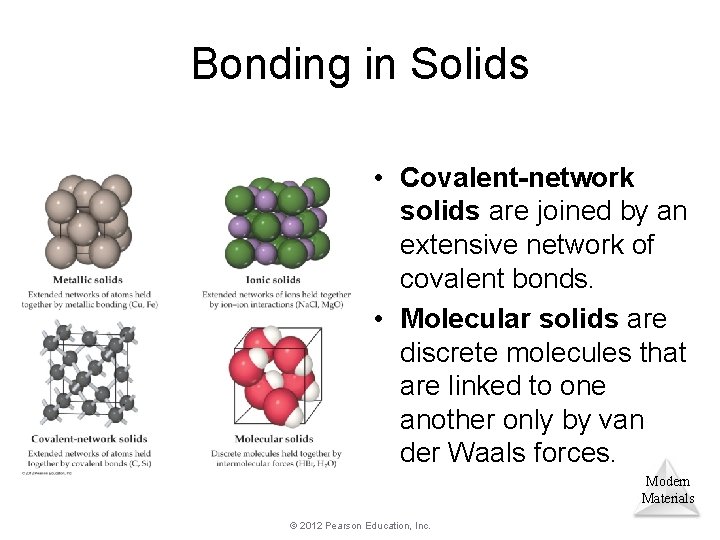
Bonding in Solids • Covalent-network solids are joined by an extensive network of covalent bonds. • Molecular solids are discrete molecules that are linked to one another only by van der Waals forces. Modern Materials © 2012 Pearson Education, Inc.

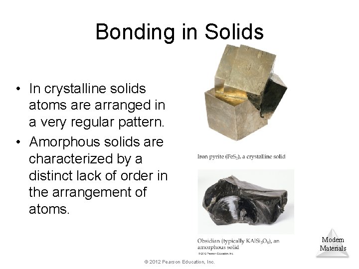
Bonding in Solids • In crystalline solids atoms are arranged in a very regular pattern. • Amorphous solids are characterized by a distinct lack of order in the arrangement of atoms. Modern Materials © 2012 Pearson Education, Inc.

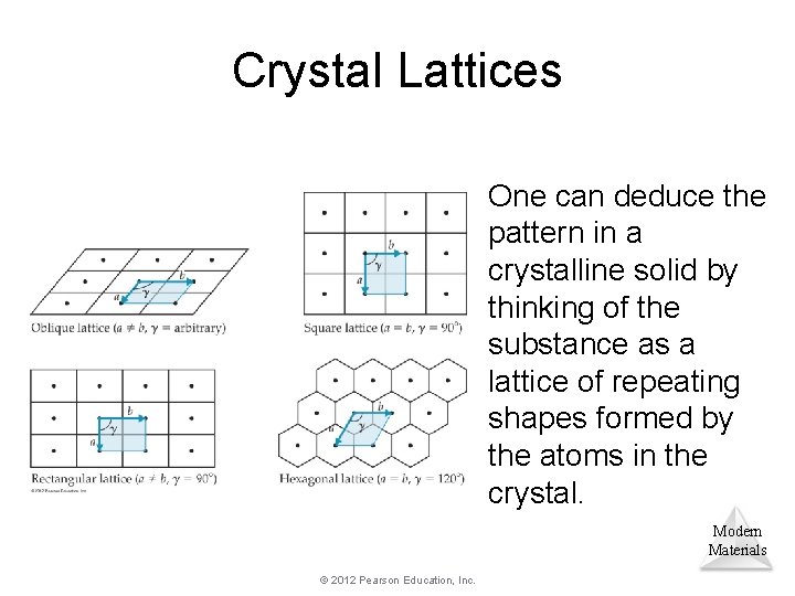
Crystal Lattices One can deduce the pattern in a crystalline solid by thinking of the substance as a lattice of repeating shapes formed by the atoms in the crystal. Modern Materials © 2012 Pearson Education, Inc.

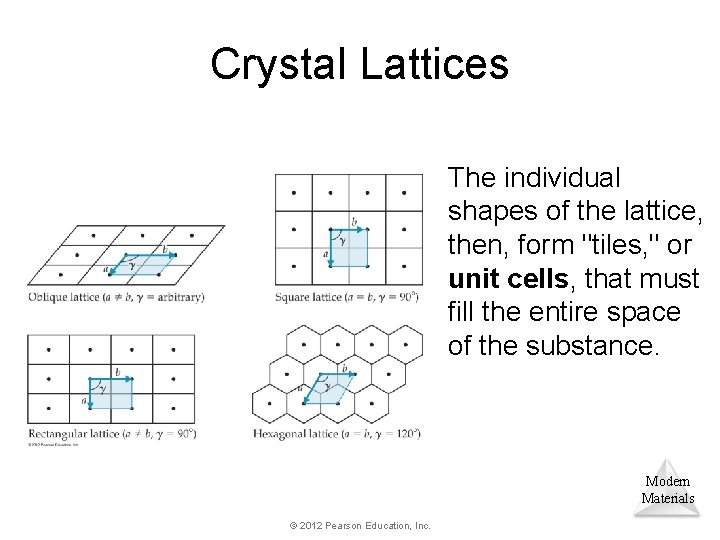
Crystal Lattices The individual shapes of the lattice, then, form "tiles, " or unit cells, that must fill the entire space of the substance. Modern Materials © 2012 Pearson Education, Inc.

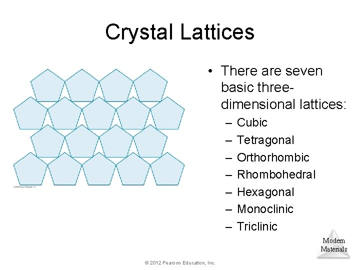
Crystal Lattices • There are seven basic threedimensional lattices: – – – – Cubic Tetragonal Orthorhombic Rhombohedral Hexagonal Monoclinic Triclinic Modern Materials © 2012 Pearson Education, Inc.

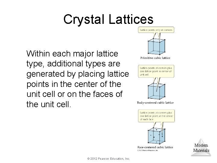
Crystal Lattices Within each major lattice type, additional types are generated by placing lattice points in the center of the unit cell or on the faces of the unit cell. Modern Materials © 2012 Pearson Education, Inc.

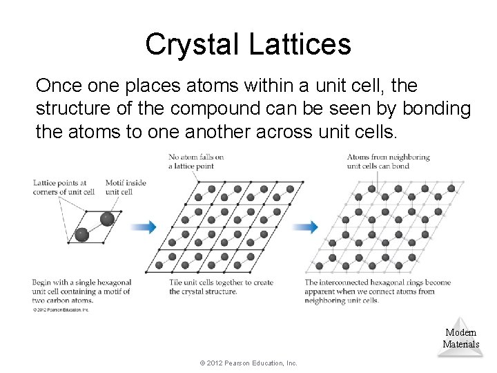
Crystal Lattices Once one places atoms within a unit cell, the structure of the compound can be seen by bonding the atoms to one another across unit cells. Modern Materials © 2012 Pearson Education, Inc.

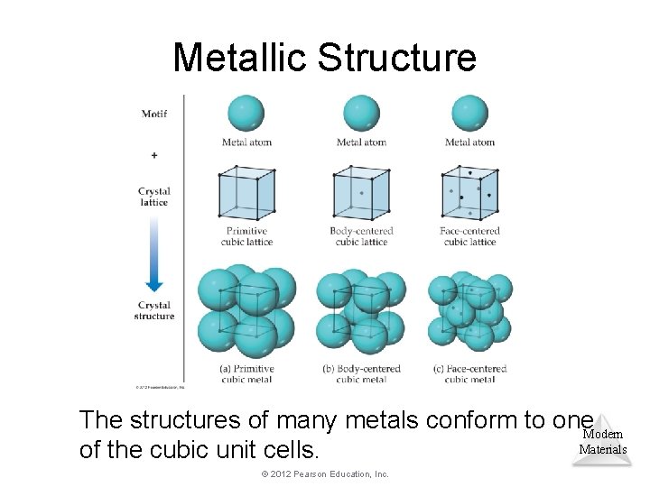
Metallic Structure The structures of many metals conform to one. Modern Materials of the cubic unit cells. © 2012 Pearson Education, Inc.

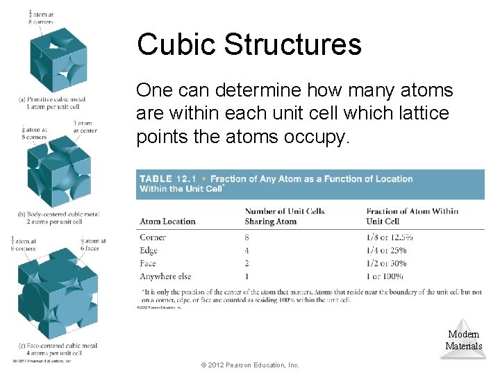
Cubic Structures One can determine how many atoms are within each unit cell which lattice points the atoms occupy. Modern Materials © 2012 Pearson Education, Inc.

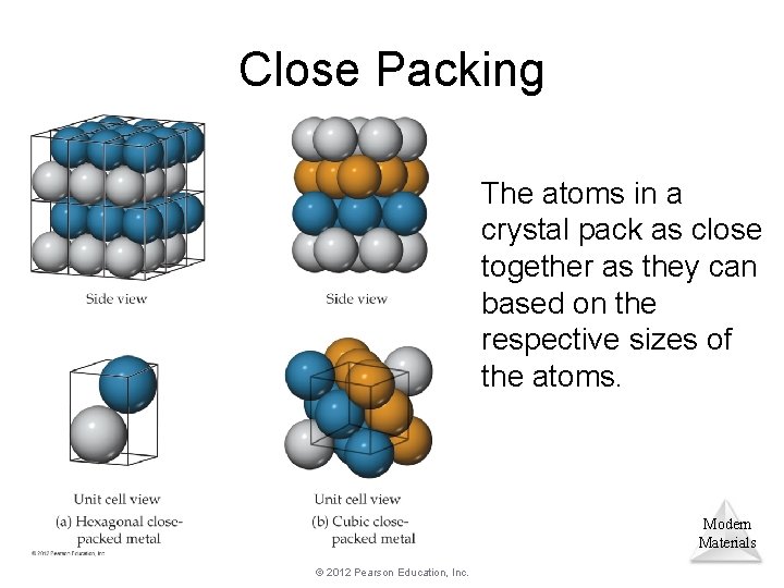
Close Packing The atoms in a crystal pack as close together as they can based on the respective sizes of the atoms. Modern Materials © 2012 Pearson Education, Inc.

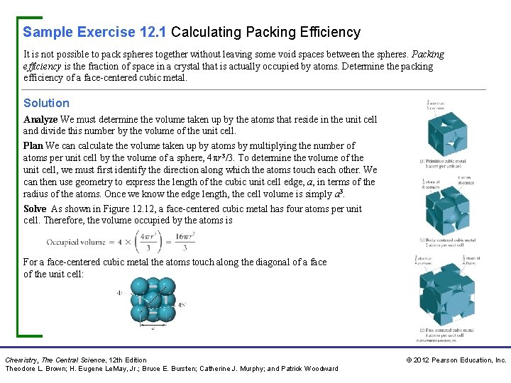
Sample Exercise 12. 1 Calculating Packing Efficiency It is not possible to pack spheres together without leaving some void spaces between the spheres. Packing efficiency is the fraction of space in a crystal that is actually occupied by atoms. Determine the packing efficiency of a face-centered cubic metal. Solution Analyze We must determine the volume taken up by the atoms that reside in the unit cell and divide this number by the volume of the unit cell. Plan We can calculate the volume taken up by atoms by multiplying the number of atoms per unit cell by the volume of a sphere, 4 r 3/3. To determine the volume of the unit cell, we must first identify the direction along which the atoms touch each other. We can then use geometry to express the length of the cubic unit cell edge, a, in terms of the radius of the atoms. Once we know the edge length, the cell volume is simply a 3. Solve As shown in Figure 12. 12, a face-centered cubic metal has four atoms per unit cell. Therefore, the volume occupied by the atoms is For a face-centered cubic metal the atoms touch along the diagonal of a face of the unit cell: Chemistry, The Central Science, 12 th Edition Theodore L. Brown; H. Eugene Le. May, Jr. ; Bruce E. Bursten; Catherine J. Murphy; and Patrick Woodward © 2012 Pearson Education, Inc.

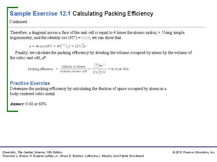
Sample Exercise 12. 1 Calculating Packing Efficiency Continued Therefore, a diagonal across a face of the unit cell is equal to 4 times the atomic radius, r. Using simple trigonometry, and the identity cos (45 ) = , we can show that Finally, we calculate the packing efficiency by dividing the volume occupied by atoms by the volume of the cubic unit cell, a 3: Practice Exercise Determine the packing efficiency by calculating the fraction of space occupied by atoms in a body-centered cubic metal. Answer: 0. 68 or 68% Chemistry, The Central Science, 12 th Edition Theodore L. Brown; H. Eugene Le. May, Jr. ; Bruce E. Bursten; Catherine J. Murphy; and Patrick Woodward © 2012 Pearson Education, Inc.

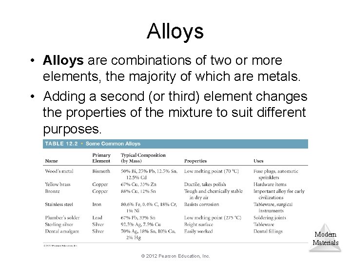
Alloys • Alloys are combinations of two or more elements, the majority of which are metals. • Adding a second (or third) element changes the properties of the mixture to suit different purposes. Modern Materials © 2012 Pearson Education, Inc.

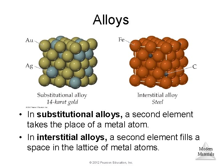
Alloys • In substitutional alloys, a second element takes the place of a metal atom. • In interstitial alloys, a second element fills a space in the lattice of metal atoms. Modern Materials © 2012 Pearson Education, Inc.

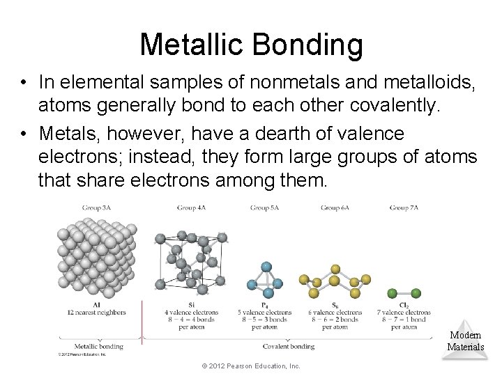
Metallic Bonding • In elemental samples of nonmetals and metalloids, atoms generally bond to each other covalently. • Metals, however, have a dearth of valence electrons; instead, they form large groups of atoms that share electrons among them. Modern Materials © 2012 Pearson Education, Inc.

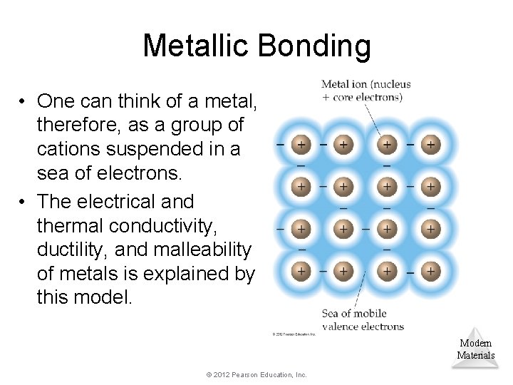
Metallic Bonding • One can think of a metal, therefore, as a group of cations suspended in a sea of electrons. • The electrical and thermal conductivity, ductility, and malleability of metals is explained by this model. Modern Materials © 2012 Pearson Education, Inc.

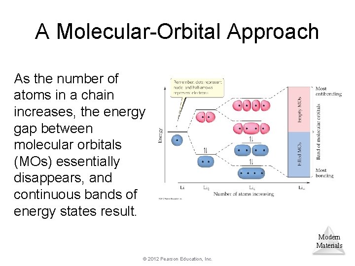
A Molecular-Orbital Approach As the number of atoms in a chain increases, the energy gap between molecular orbitals (MOs) essentially disappears, and continuous bands of energy states result. Modern Materials © 2012 Pearson Education, Inc.

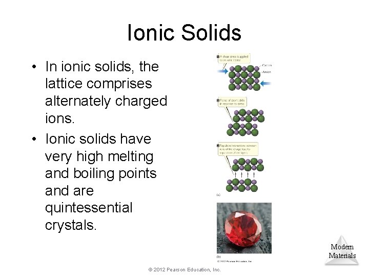
Ionic Solids • In ionic solids, the lattice comprises alternately charged ions. • Ionic solids have very high melting and boiling points and are quintessential crystals. Modern Materials © 2012 Pearson Education, Inc.

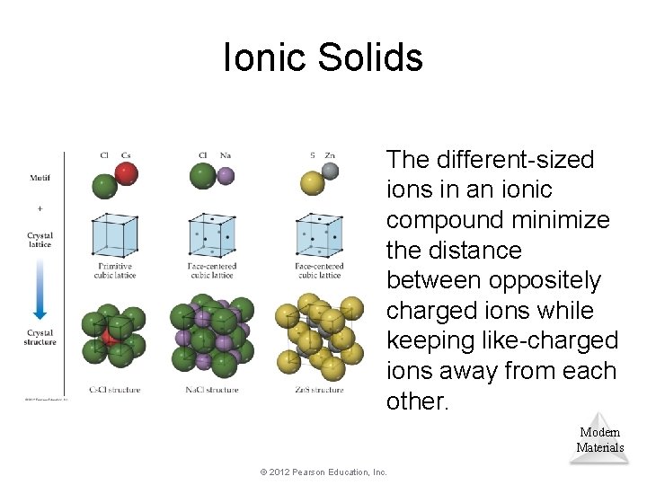
Ionic Solids The different-sized ions in an ionic compound minimize the distance between oppositely charged ions while keeping like-charged ions away from each other. Modern Materials © 2012 Pearson Education, Inc.

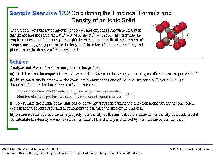
Sample Exercise 12. 2 Calculating the Empirical Formula and Density of an Ionic Solid The unit cell of a binary compound of copper and oxygen is shown here. Given this image and the ionic radii r. Cu+ = 0. 74 Å and r. O 2 = 1. 26 Å, (a) determine the empirical formula of this compound, (b) determine the coordination numbers of copper and oxygen, (c) estimate the length of the edge of the cubic unit cell, and (d) estimate the density of the compound. Solution Analyze and Plan There are four parts to this problem. (a) To determine the empirical formula we need to determine how many of each type of ion there are per unit cell. (b) If we can visually determine the coordination number of one of the ions, we can use Equation 12. 1 to determine the coordination number of the other ion. (c) To estimate the length of the unit cell edge we must first determine the direction along which the ions touch. We can then use ionic radii and trigonometry to estimate the size of the unit cell. (d) Because density is an intensive property, the density of the unit cell is the same as the density of a bulk crystal. To calculate the density we must divide the mass of the atoms per unit cell by the volume of the unit cell. Chemistry, The Central Science, 12 th Edition Theodore L. Brown; H. Eugene Le. May, Jr. ; Bruce E. Bursten; Catherine J. Murphy; and Patrick Woodward © 2012 Pearson Education, Inc.

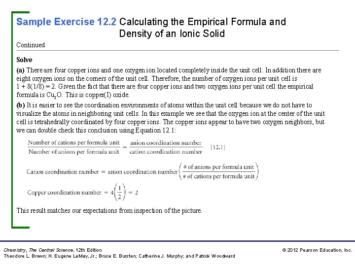
Sample Exercise 12. 2 Calculating the Empirical Formula and Density of an Ionic Solid Continued Solve (a) There are four copper ions and one oxygen ion located completely inside the unit cell. In addition there are eight oxygen ions on the corners of the unit cell. Therefore, the number of oxygen ions per unit cell is 1 + 8(1/8) = 2. Given the fact that there are four copper ions and two oxygen ions per unit cell the empirical formula is Cu 2 O. This is copper(I) oxide. (b) It is easier to see the coordination environments of atoms within the unit cell because we do not have to visualize the atoms in neighboring unit cells. In this example we see that the oxygen ion at the center of the unit cell is tetrahedrally coordinated by four copper ions. The copper ions appear to have two oxygen neighbors, but we can double check this conclusion using Equation 12. 1: This result matches our expectations from inspection of the picture. Chemistry, The Central Science, 12 th Edition Theodore L. Brown; H. Eugene Le. May, Jr. ; Bruce E. Bursten; Catherine J. Murphy; and Patrick Woodward © 2012 Pearson Education, Inc.

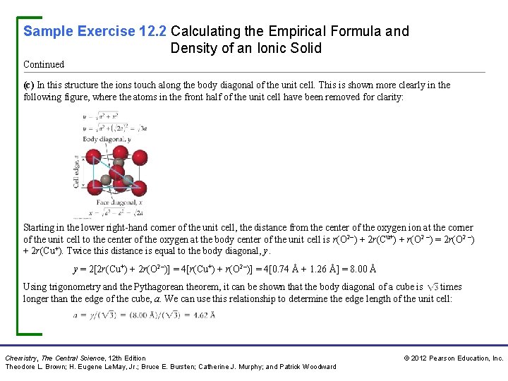
Sample Exercise 12. 2 Calculating the Empirical Formula and Density of an Ionic Solid Continued (c) In this structure the ions touch along the body diagonal of the unit cell. This is shown more clearly in the following figure, where the atoms in the front half of the unit cell have been removed for clarity: Starting in the lower right-hand corner of the unit cell, the distance from the center of the oxygen ion at the corner of the unit cell to the center of the oxygen at the body center of the unit cell is r(O 2 ) + 2 r(Cu+) + r(O 2 ) = 2 r(O 2 ) + 2 r(Cu+). Twice this distance is equal to the body diagonal, y. y = 2[2 r(Cu+) + 2 r(O 2 )] = 4[r(Cu+) + r(O 2 )] = 4[0. 74 Å + 1. 26 Å] = 8. 00 Å Using trigonometry and the Pythagorean theorem, it can be shown that the body diagonal of a cube is times longer than the edge of the cube, a. We can use this relationship to determine the edge length of the unit cell: Chemistry, The Central Science, 12 th Edition Theodore L. Brown; H. Eugene Le. May, Jr. ; Bruce E. Bursten; Catherine J. Murphy; and Patrick Woodward © 2012 Pearson Education, Inc.

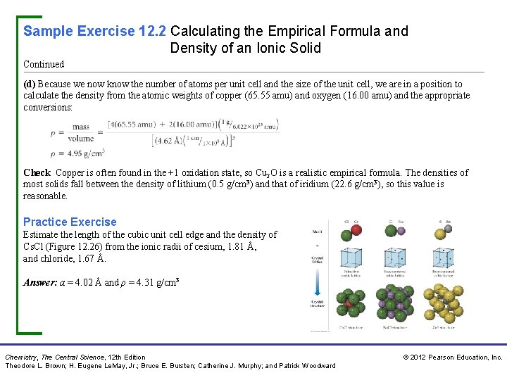
Sample Exercise 12. 2 Calculating the Empirical Formula and Density of an Ionic Solid Continued (d) Because we now know the number of atoms per unit cell and the size of the unit cell, we are in a position to calculate the density from the atomic weights of copper (65. 55 amu) and oxygen (16. 00 amu) and the appropriate conversions: Check Copper is often found in the +1 oxidation state, so Cu 2 O is a realistic empirical formula. The densities of most solids fall between the density of lithium (0. 5 g/cm 3) and that of iridium (22. 6 g/cm 3), so this value is reasonable. Practice Exercise Estimate the length of the cubic unit cell edge and the density of Cs. Cl (Figure 12. 26) from the ionic radii of cesium, 1. 81 Å, and chloride, 1. 67 Å. Answer: a = 4. 02 Å and ρ = 4. 31 g/cm 3 Chemistry, The Central Science, 12 th Edition Theodore L. Brown; H. Eugene Le. May, Jr. ; Bruce E. Bursten; Catherine J. Murphy; and Patrick Woodward © 2012 Pearson Education, Inc.

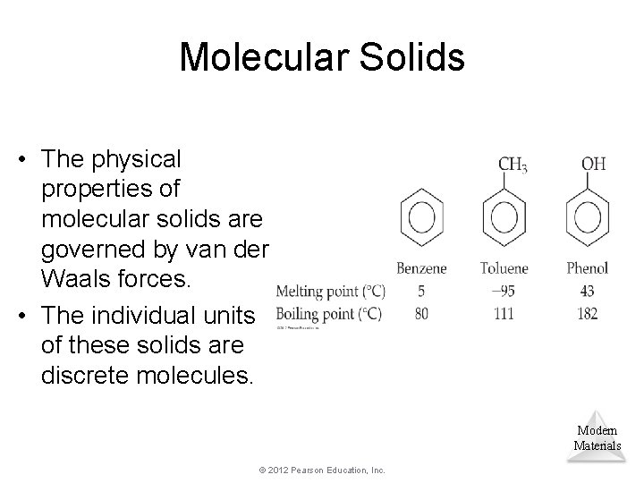
Molecular Solids • The physical properties of molecular solids are governed by van der Waals forces. • The individual units of these solids are discrete molecules. Modern Materials © 2012 Pearson Education, Inc.

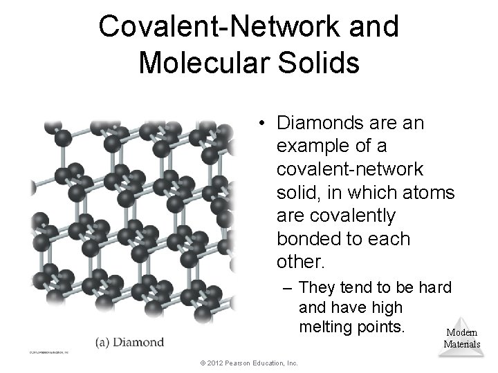
Covalent-Network and Molecular Solids • Diamonds are an example of a covalent-network solid, in which atoms are covalently bonded to each other. – They tend to be hard and have high melting points. Modern Materials © 2012 Pearson Education, Inc.

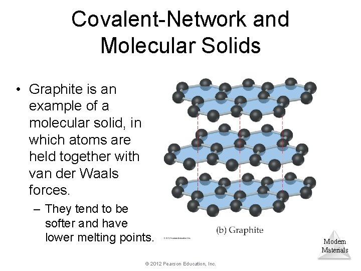
Covalent-Network and Molecular Solids • Graphite is an example of a molecular solid, in which atoms are held together with van der Waals forces. – They tend to be softer and have lower melting points. © 2012 Pearson Education, Inc. Modern Materials

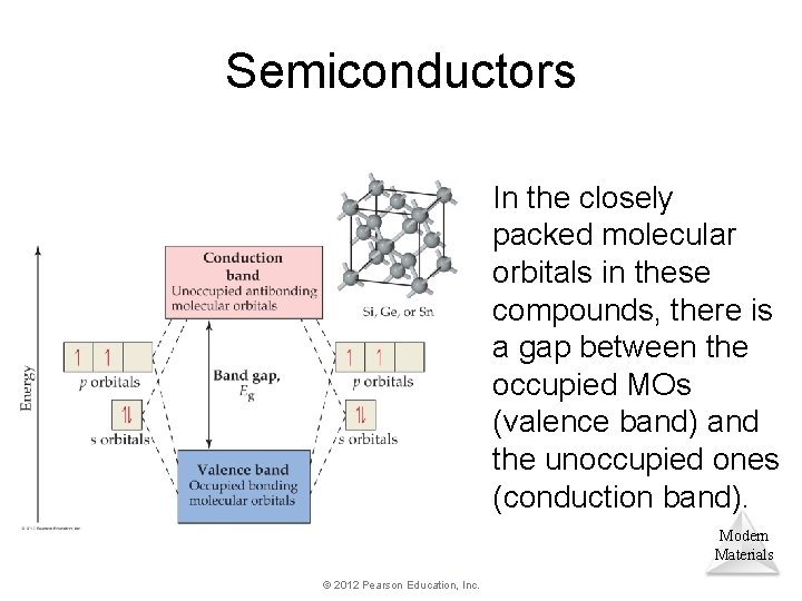
Semiconductors In the closely packed molecular orbitals in these compounds, there is a gap between the occupied MOs (valence band) and the unoccupied ones (conduction band). Modern Materials © 2012 Pearson Education, Inc.

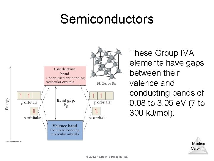
Semiconductors These Group IVA elements have gaps between their valence and conducting bands of 0. 08 to 3. 05 e. V (7 to 300 k. J/mol). Modern Materials © 2012 Pearson Education, Inc.

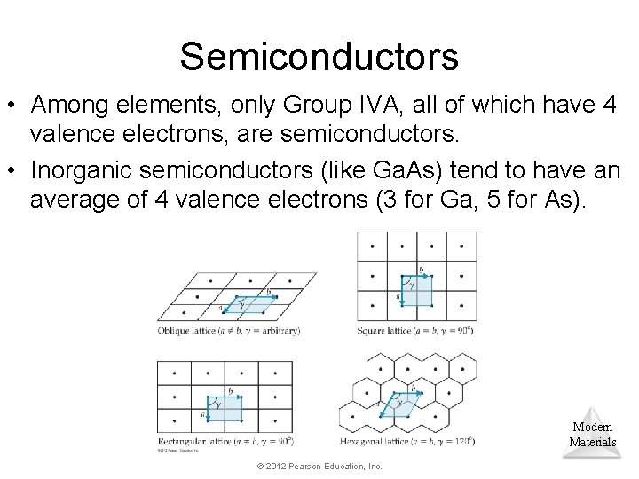
Semiconductors • Among elements, only Group IVA, all of which have 4 valence electrons, are semiconductors. • Inorganic semiconductors (like Ga. As) tend to have an average of 4 valence electrons (3 for Ga, 5 for As). Modern Materials © 2012 Pearson Education, Inc.

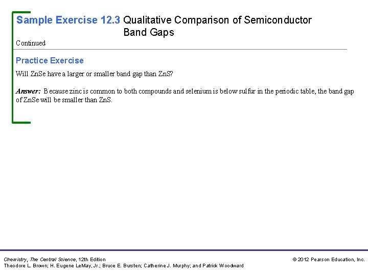
Sample Exercise 12. 3 Qualitative Comparison of Semiconductor Band Gaps Will Ga. P have a larger or smaller band gap than Zn. S? Will it have a larger or smaller band gap than Ga. N? Solution Analyze The size of the band gap depends on the vertical and horizontal positions of the elements in the periodic table. The band gap will increase when either of the following conditions is met: (1) The elements are located higher up in the periodic table, where enhanced orbital overlap leads to a larger splitting between bonding and antibonding orbitals, or (2) the horizontal separation between the elements increases, which leads to an increase in the electronegativity difference and bond polarity. Plan We must look at the periodic table and compare the relative positions of the elements in each case. Solve Gallium is in the fourth period and group 3 A. Phosphorus is in the third period and group 5 A. Zinc and sulfur are in the same periods as gallium and phosphorus, respectively. However, zinc, in group 2 B, is one element to the left of gallium; sulfur in group 6 A is one element to the right of phosphorus. Thus, we would expect the electronegativity difference to be larger for Zn. S, which should result in Zn. S having a larger band gap than Ga. P. For both Ga. P and Ga. N the more electropositive element is gallium. So we need only compare the positions of the more electronegative elements, P and N. Nitrogen is located above phosphorus in group 5 A. Therefore, based on increased orbital overlap, we would expect Ga. N to have a larger band gap than Ga. P. Check External references show that the band gap of Ga. P is 2. 26 e. V, Zn. S is 3. 6 e. V, and Ga. N is 3. 4 e. V. Chemistry, The Central Science, 12 th Edition Theodore L. Brown; H. Eugene Le. May, Jr. ; Bruce E. Bursten; Catherine J. Murphy; and Patrick Woodward © 2012 Pearson Education, Inc.

Sample Exercise 12. 3 Qualitative Comparison of Semiconductor Band Gaps Continued Practice Exercise Will Zn. Se have a larger or smaller band gap than Zn. S? Answer: Because zinc is common to both compounds and selenium is below sulfur in the periodic table, the band gap of Zn. Se will be smaller than Zn. S. Chemistry, The Central Science, 12 th Edition Theodore L. Brown; H. Eugene Le. May, Jr. ; Bruce E. Bursten; Catherine J. Murphy; and Patrick Woodward © 2012 Pearson Education, Inc.

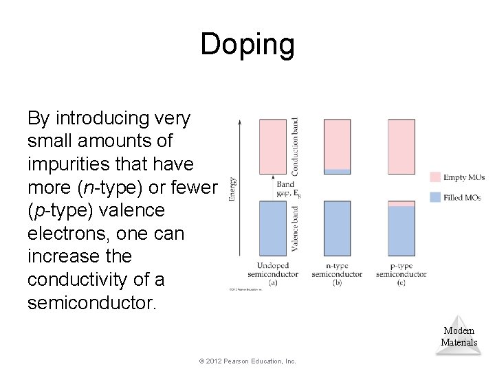
Doping By introducing very small amounts of impurities that have more (n-type) or fewer (p-type) valence electrons, one can increase the conductivity of a semiconductor. Modern Materials © 2012 Pearson Education, Inc.

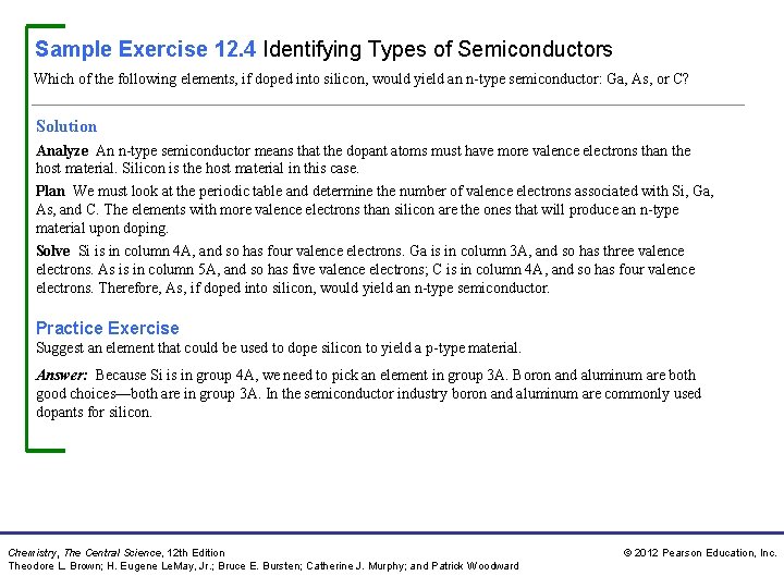
Sample Exercise 12. 4 Identifying Types of Semiconductors Which of the following elements, if doped into silicon, would yield an n-type semiconductor: Ga, As, or C? Solution Analyze An n-type semiconductor means that the dopant atoms must have more valence electrons than the host material. Silicon is the host material in this case. Plan We must look at the periodic table and determine the number of valence electrons associated with Si, Ga, As, and C. The elements with more valence electrons than silicon are the ones that will produce an n-type material upon doping. Solve Si is in column 4 A, and so has four valence electrons. Ga is in column 3 A, and so has three valence electrons. As is in column 5 A, and so has five valence electrons; C is in column 4 A, and so has four valence electrons. Therefore, As, if doped into silicon, would yield an n-type semiconductor. Practice Exercise Suggest an element that could be used to dope silicon to yield a p-type material. Answer: Because Si is in group 4 A, we need to pick an element in group 3 A. Boron and aluminum are both good choices—both are in group 3 A. In the semiconductor industry boron and aluminum are commonly used dopants for silicon. Chemistry, The Central Science, 12 th Edition Theodore L. Brown; H. Eugene Le. May, Jr. ; Bruce E. Bursten; Catherine J. Murphy; and Patrick Woodward © 2012 Pearson Education, Inc.

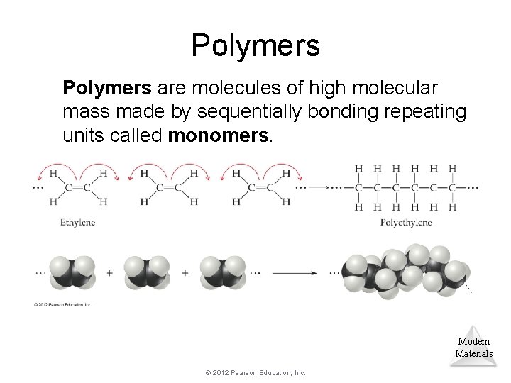
Polymers are molecules of high molecular mass made by sequentially bonding repeating units called monomers. Modern Materials © 2012 Pearson Education, Inc.

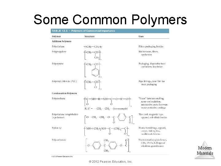
Some Common Polymers Modern Materials © 2012 Pearson Education, Inc.

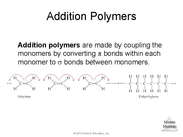
Addition Polymers Addition polymers are made by coupling the monomers by converting bonds within each monomer to bonds between monomers. Modern Materials © 2012 Pearson Education, Inc.

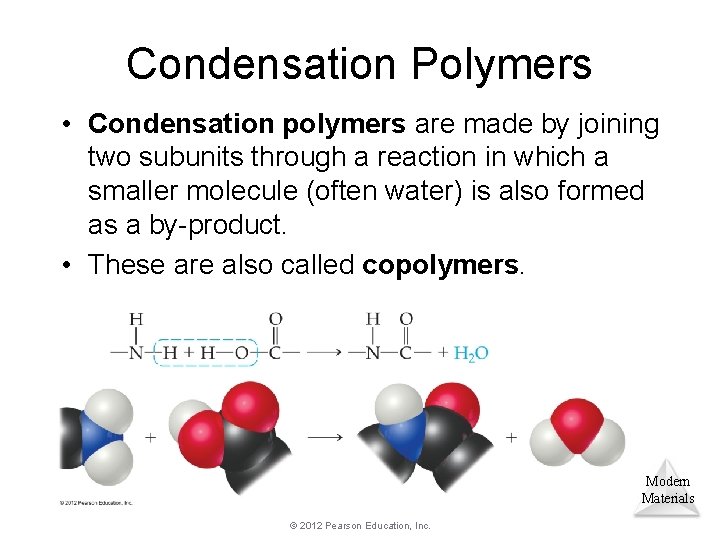
Condensation Polymers • Condensation polymers are made by joining two subunits through a reaction in which a smaller molecule (often water) is also formed as a by-product. • These are also called copolymers. Modern Materials © 2012 Pearson Education, Inc.

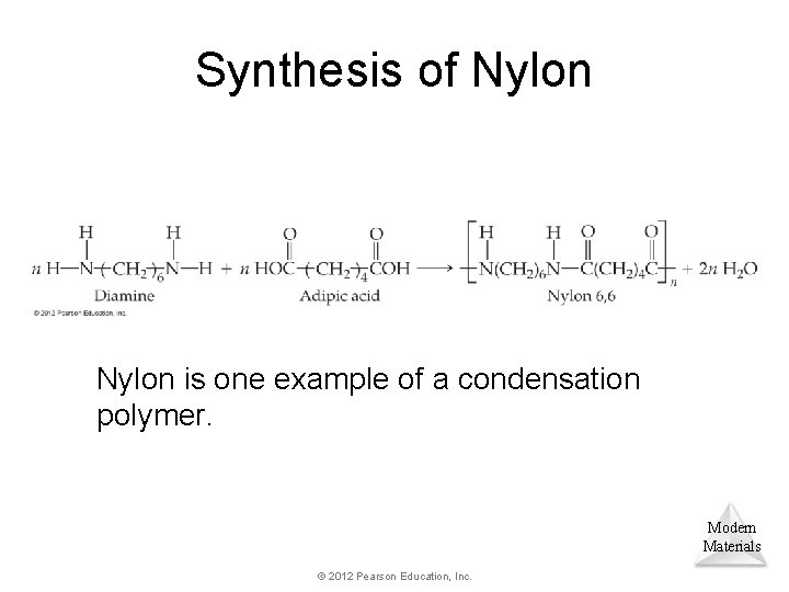
Synthesis of Nylon is one example of a condensation polymer. Modern Materials © 2012 Pearson Education, Inc.

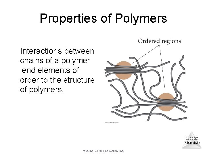
Properties of Polymers Interactions between chains of a polymer lend elements of order to the structure of polymers. Modern Materials © 2012 Pearson Education, Inc.

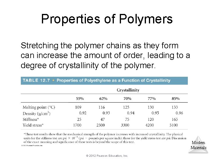
Properties of Polymers Stretching the polymer chains as they form can increase the amount of order, leading to a degree of crystallinity of the polymer. Modern Materials © 2012 Pearson Education, Inc.

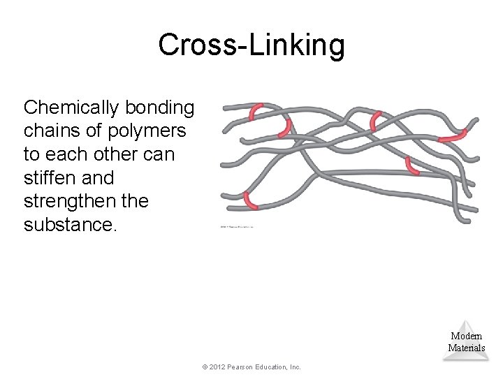
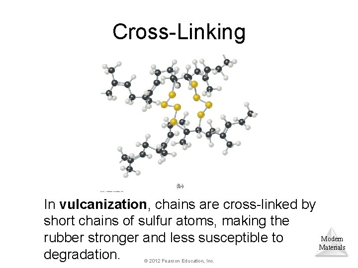
Cross-Linking Chemically bonding chains of polymers to each other can stiffen and strengthen the substance. Modern Materials © 2012 Pearson Education, Inc.

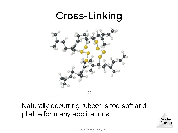
Cross-Linking Naturally occurring rubber is too soft and pliable for many applications. © 2012 Pearson Education, Inc. Modern Materials

Cross-Linking In vulcanization, chains are cross-linked by short chains of sulfur atoms, making the Modern rubber stronger and less susceptible to Materials degradation. © 2012 Pearson Education, Inc.

End of Today’s Notes Homework: 1. Read chapter 12 (again) 2. Complete chapter 12 activity on Mastering Chemistry 3. Study for Unit 3 test covering chapters 10, 11, and 12 Modern Materials © 2012 Pearson Education, Inc.