Lecture 2 1 Crystalline Solids Crystalline Solids Polycrystalline


 l Lattice is constructed of repeated unit cells l Lattice Point")

 Family of Miller Planes {hkl}")


 – ao=")


 X-rays of Single l All (hkl) planes are exposed at")


 --(447ºC)-> Ca(bcc)")


- Slides: 27
Lecture 2. 1 Crystalline Solids
Crystalline Solids Poly-crystalline solids - Grains l Mono-crystalline solids- Whiskers, Wafers l
Crystal Lattices
Crystal Systems =>14 Bravais Lattices
Bravais lattice (abc) l Lattice is constructed of repeated unit cells l Lattice Point - 1/3 a, 1/2 b, 1/4 c l Crystallographic Direction (vector from 0, 0, 0 to xyz) which is defined by – [uvw] smallest set of integers having the same ratio as xyz – bar over number = minus number
Close Packed Structures l Cubic, BCC, FCC, HCC are the focus of this course l Determining distances and volume fractions in Cubic Structures
Miller indices for a plane (hkl) Family of Miller Planes {hkl}
EXAMPLE- Miller Index l l l intercepts on a, b&c axes=3, 1&2, respectively reciprocals = 1/3, 1/1&1/2, respectively smallest set of integers with same common ratio = 2, 6&3 Miller indexes of Plane, (hkl)=(263) also called “reciprocal space plane”
Family of Planes {110}
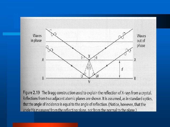
Measuring Structure with X-rays l Generate l X-ray radiation Diffraction ( =90) – ao= cubic lattice parameter
X-Ray Generation l Electron Scattering – Broad Band X-rays l Electron Kickout – K, L, M shell electron – Replace with higher electron – Transition gives Xrays • one wave length l K , L , L K K
X-ray Generation Energy Level Diagrams -0. 85 e. V -1. 51 e. V 4 3 K 2 L L L -3. 40 e. V K 1 K -13. 6 e. V
X-ray Camera-1 l Single Crystal Camera – Broad Band X-rays – all in source – only Bragg (diffracting) wavelengths reflect
Si. Ge Crystal
X-ray Camera-2 (film strip) X-rays of Single l All (hkl) planes are exposed at all angles at all times l Diffraction of Bragg planes l
Electron Diffraction Focused Electrons of different energy l Transmission through sample l CCD detector l Thinned Sample CCD Detector
Seeing Crystal Structure with and Atomic Force Microscope l Electron Microscope l Atomic Force Microscope l Scanning Tunneling Microscope
Diffracting Planes
Changing Crystal Structure – Allotropic Phase Change HCP->FCC->BCC->SC l l l Ca(fcc) --(447ºC)-> Ca(bcc) Co(hcp) --(427ºC)--> Co(fcc) Fe(bcc) --(912ºC)-->Fe(fcc) --(1394ºC)-->Fe(hcp) Na(bcc) --(-233ºC)--> Na(hcp) Ti(hcp) --(883ºC)-->Ti(bcc) Zr(hcp) --(872ºC)--> Zr(bcc) Decreasing density with increasing temperature!
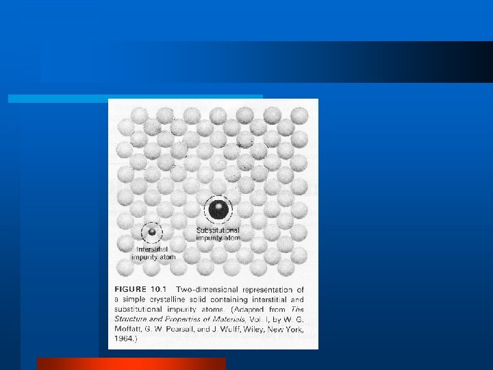
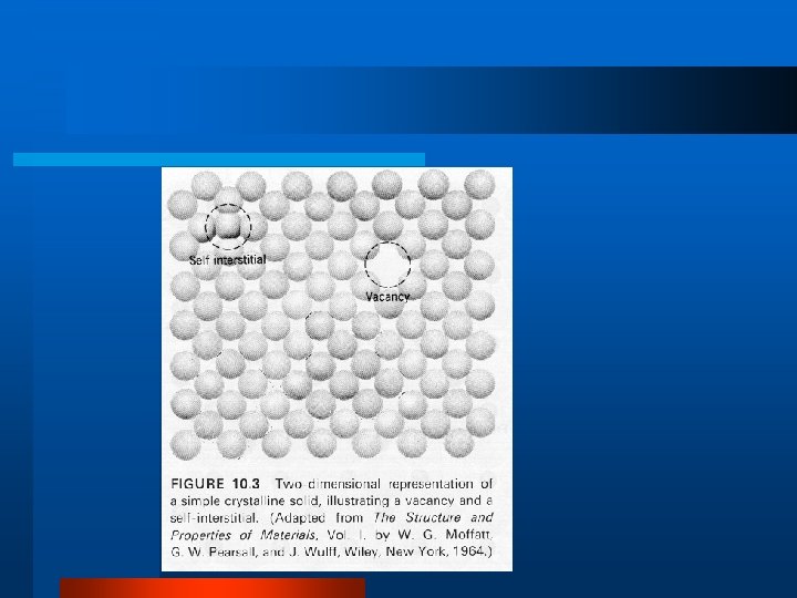
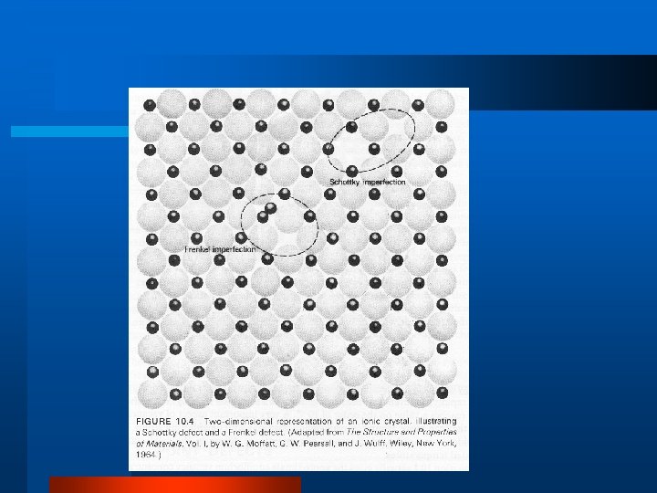
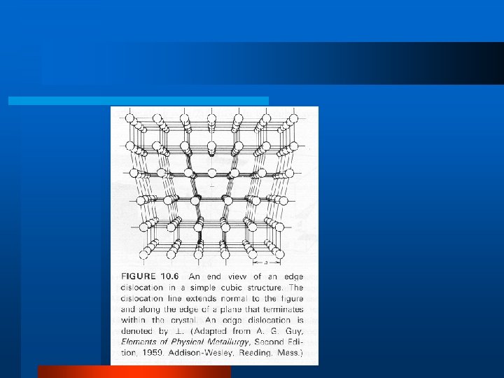
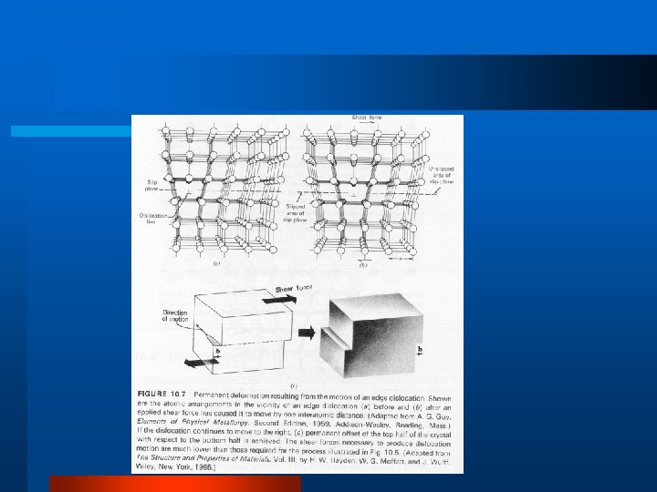
Defects in Crystal Structure l Vacancy, Interstitial, Impurity l Schottky Defect l Frenkel Defect l Dislocations – edge dislocation, line, screw l Grain Boundary
Effect of Structure on Mechanical Properties l Elasticity l Plastic Deformation