Chapter 12 Solids and Modern Materials 2015 Pearson
- Slides: 38

Chapter 12 Solids and Modern Materials © 2015 Pearson Education, Inc.

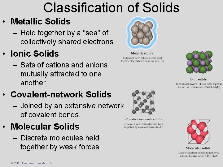
Classification of Solids • Metallic Solids – Held together by a “sea” of collectively shared electrons. • Ionic Solids – Sets of cations and anions mutually attracted to one another. • Covalent-network Solids – Joined by an extensive network of covalent bonds. • Molecular Solids – Discrete molecules held together by weak forces. © 2015 Pearson Education, Inc.

Classification of Solids • Polymers – Long chains of atoms connected by covalent bonds – Chains can be connected to other chains by weak forces. – Different properties than small molecules or metallic or ionic compounds. • Nanomaterials – Crystalline compounds with the crystals on the order of 1– 100 nm – Very different properties than larger crystalline materials. © 2015 Pearson Education, Inc.

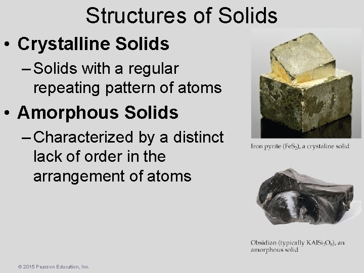
Structures of Solids • Crystalline Solids – Solids with a regular repeating pattern of atoms • Amorphous Solids – Characterized by a distinct lack of order in the arrangement of atoms © 2015 Pearson Education, Inc.

Structures of Solids • Unit Cell – The basis of a repeating pattern • The structure of a crystalline solid is defined by – the size and shape of the unit cell. – the locations of atoms within the unit cell. © 2015 Pearson Education, Inc.

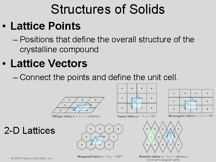
Structures of Solids • Lattice Points – Positions that define the overall structure of the crystalline compound • Lattice Vectors – Connect the points and define the unit cell. 2 -D Lattices © 2015 Pearson Education, Inc.

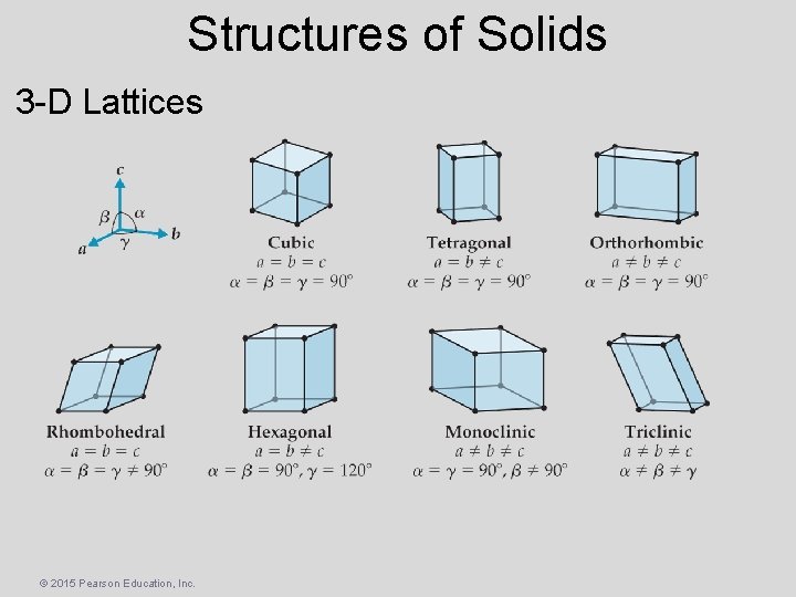
Structures of Solids 3 -D Lattices © 2015 Pearson Education, Inc.

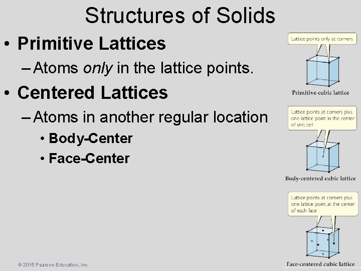
Structures of Solids • Primitive Lattices – Atoms only in the lattice points. • Centered Lattices – Atoms in another regular location • Body-Center • Face-Center © 2015 Pearson Education, Inc.

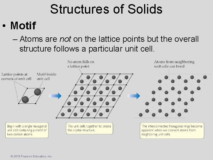
Structures of Solids • Motif – Atoms are not on the lattice points but the overall structure follows a particular unit cell. © 2015 Pearson Education, Inc.

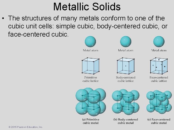
Metallic Solids • The structures of many metals conform to one of the cubic unit cells: simple cubic, body-centered cubic, or face-centered cubic. © 2015 Pearson Education, Inc.

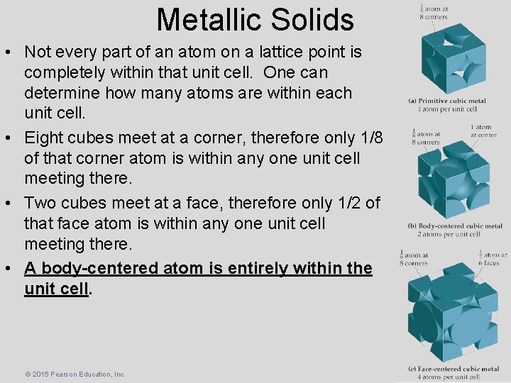
Metallic Solids • Not every part of an atom on a lattice point is completely within that unit cell. One can determine how many atoms are within each unit cell. • Eight cubes meet at a corner, therefore only 1/8 of that corner atom is within any one unit cell meeting there. • Two cubes meet at a face, therefore only 1/2 of that face atom is within any one unit cell meeting there. • A body-centered atom is entirely within the unit cell. © 2015 Pearson Education, Inc.

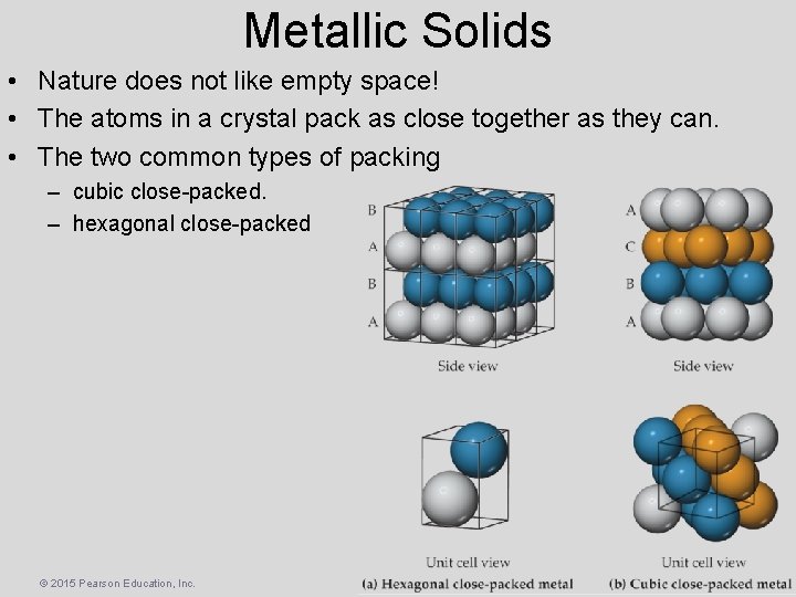
Metallic Solids • Nature does not like empty space! • The atoms in a crystal pack as close together as they can. • The two common types of packing – cubic close-packed. – hexagonal close-packed © 2015 Pearson Education, Inc.

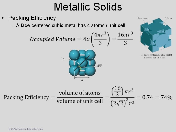
Metallic Solids • Packing Efficiency – A face-centered cubic metal has 4 atoms / unit cell. © 2015 Pearson Education, Inc.

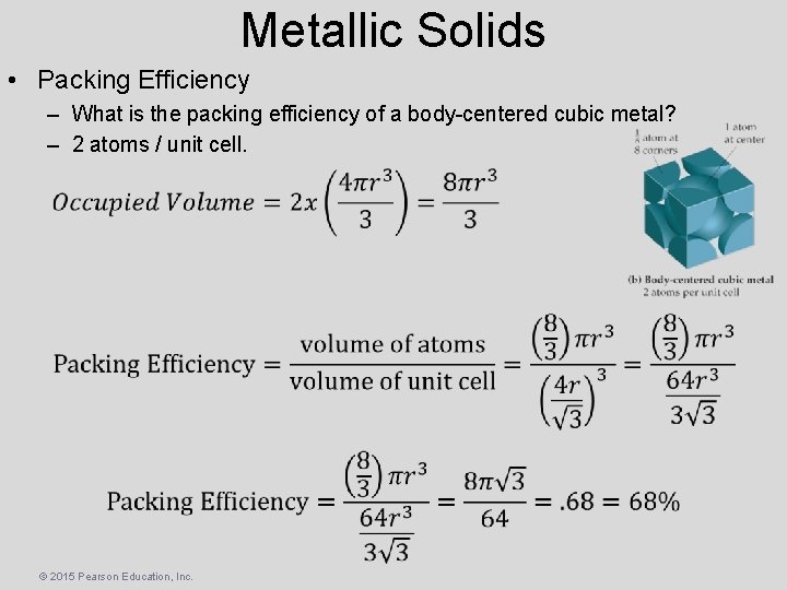
Metallic Solids • Packing Efficiency – What is the packing efficiency of a body-centered cubic metal? – 2 atoms / unit cell. © 2015 Pearson Education, Inc.

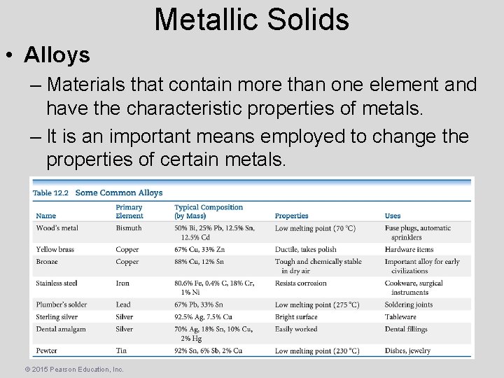
Metallic Solids • Alloys – Materials that contain more than one element and have the characteristic properties of metals. – It is an important means employed to change the properties of certain metals. © 2015 Pearson Education, Inc.

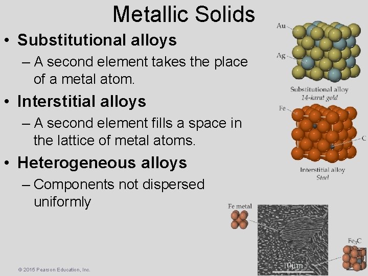
Metallic Solids • Substitutional alloys – A second element takes the place of a metal atom. • Interstitial alloys – A second element fills a space in the lattice of metal atoms. • Heterogeneous alloys – Components not dispersed uniformly © 2015 Pearson Education, Inc.

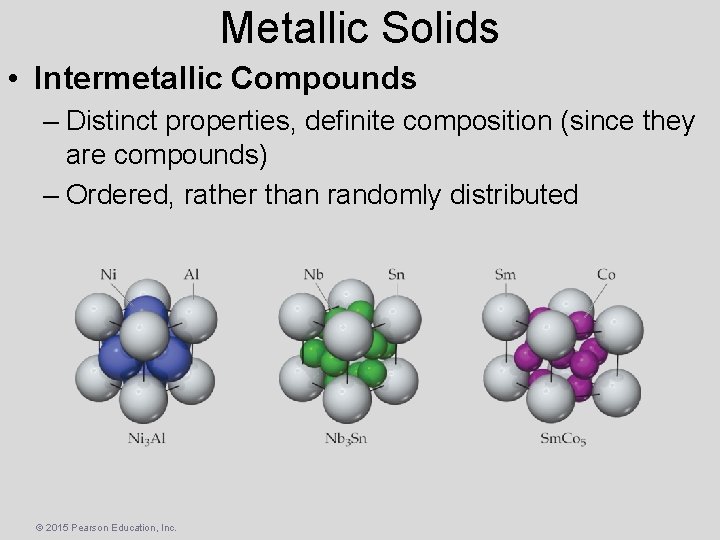
Metallic Solids • Intermetallic Compounds – Distinct properties, definite composition (since they are compounds) – Ordered, rather than randomly distributed © 2015 Pearson Education, Inc.

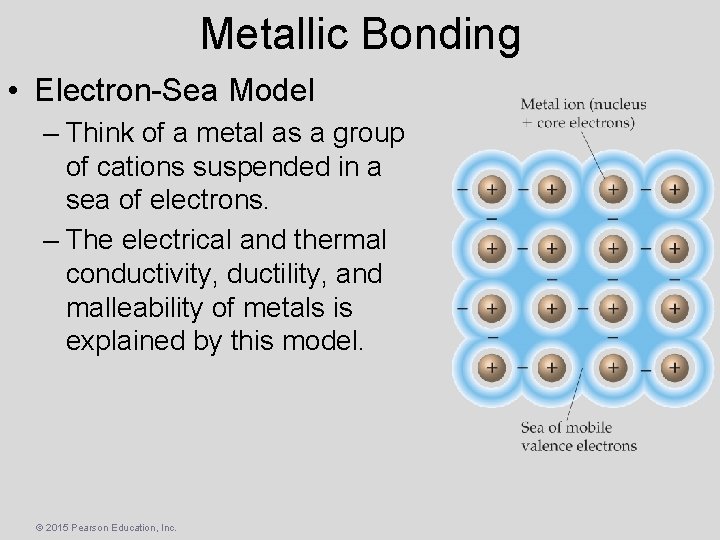
Metallic Bonding • Electron-Sea Model – Think of a metal as a group of cations suspended in a sea of electrons. – The electrical and thermal conductivity, ductility, and malleability of metals is explained by this model. © 2015 Pearson Education, Inc.

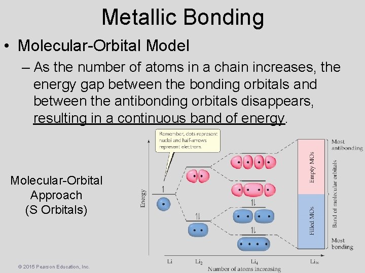
Metallic Bonding • Molecular-Orbital Model – As the number of atoms in a chain increases, the energy gap between the bonding orbitals and between the antibonding orbitals disappears, resulting in a continuous band of energy. Molecular-Orbital Approach (S Orbitals) © 2015 Pearson Education, Inc.

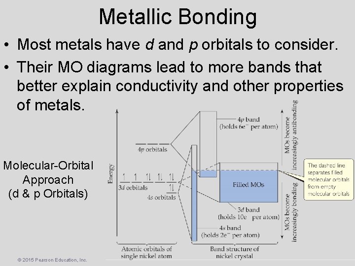
Metallic Bonding • Most metals have d and p orbitals to consider. • Their MO diagrams lead to more bands that better explain conductivity and other properties of metals. Molecular-Orbital Approach (d & p Orbitals) © 2015 Pearson Education, Inc.

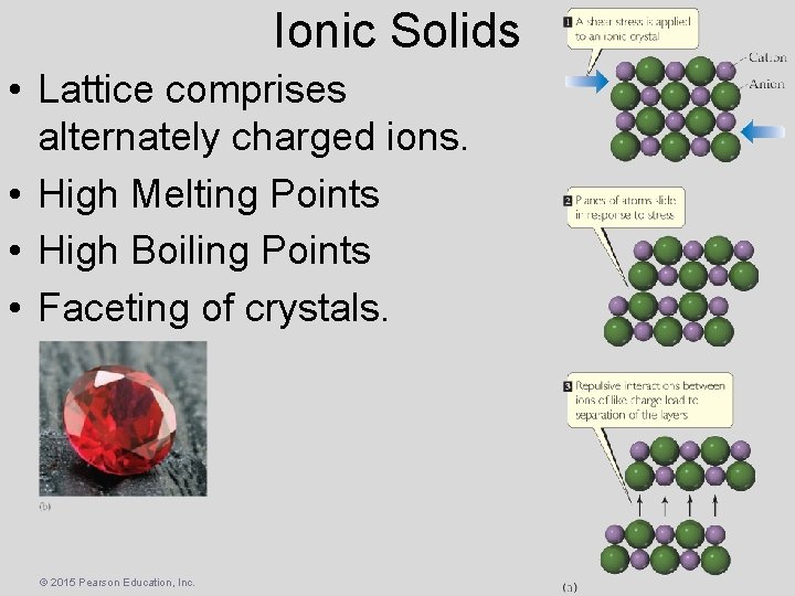
Ionic Solids • Lattice comprises alternately charged ions. • High Melting Points • High Boiling Points • Faceting of crystals. © 2015 Pearson Education, Inc.

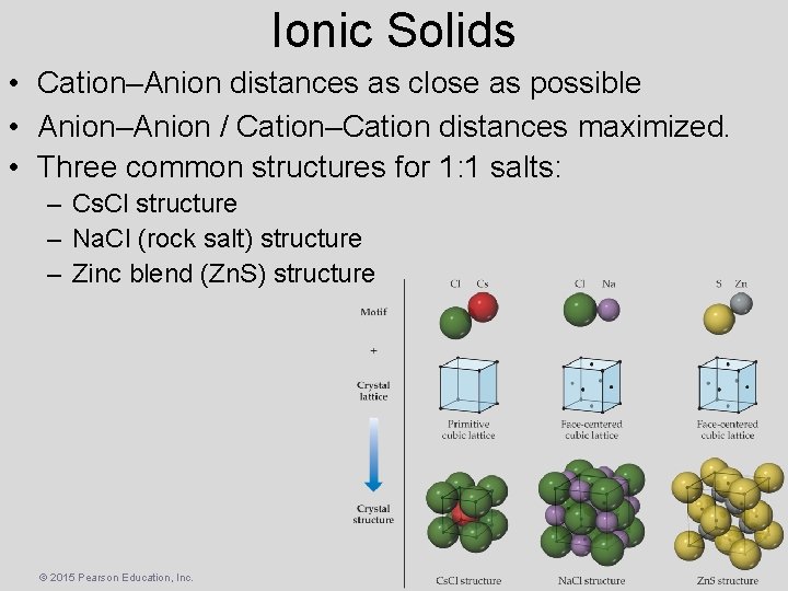
Ionic Solids • Cation–Anion distances as close as possible • Anion–Anion / Cation–Cation distances maximized. • Three common structures for 1: 1 salts: – Cs. Cl structure – Na. Cl (rock salt) structure – Zinc blend (Zn. S) structure © 2015 Pearson Education, Inc.

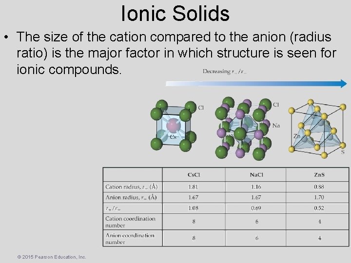
Ionic Solids • The size of the cation compared to the anion (radius ratio) is the major factor in which structure is seen for ionic compounds. © 2015 Pearson Education, Inc.

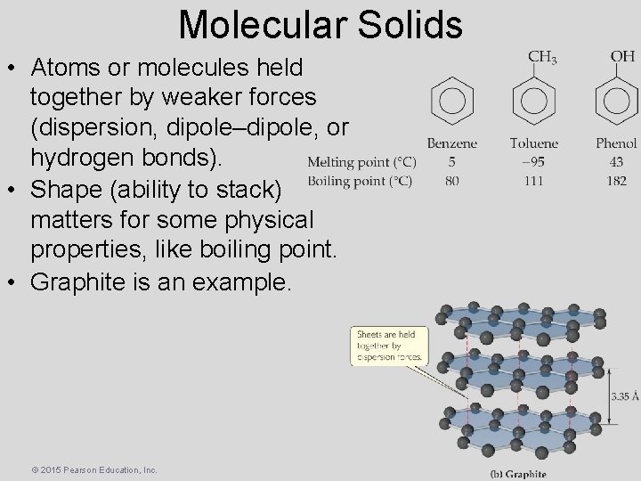
Molecular Solids • Atoms or molecules held together by weaker forces (dispersion, dipole–dipole, or hydrogen bonds). • Shape (ability to stack) matters for some physical properties, like boiling point. • Graphite is an example. © 2015 Pearson Education, Inc.

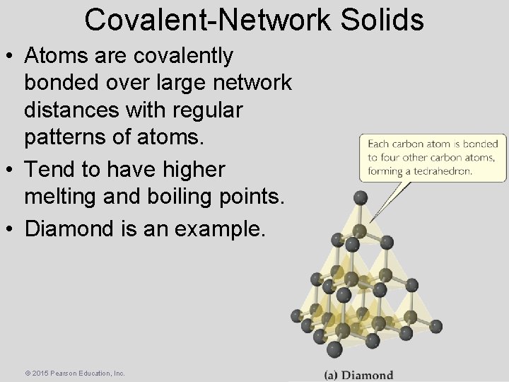
Covalent-Network Solids • Atoms are covalently bonded over large network distances with regular patterns of atoms. • Tend to have higher melting and boiling points. • Diamond is an example. © 2015 Pearson Education, Inc.

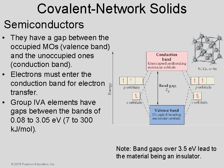
Covalent-Network Solids Semiconductors • They have a gap between the occupied MOs (valence band) and the unoccupied ones (conduction band). • Electrons must enter the conduction band for electron transfer. • Group IVA elements have gaps between the bands of 0. 08 to 3. 05 e. V (7 to 300 k. J/mol). Note: Band gaps over 3. 5 e. V lead to the material being an insulator. © 2015 Pearson Education, Inc.

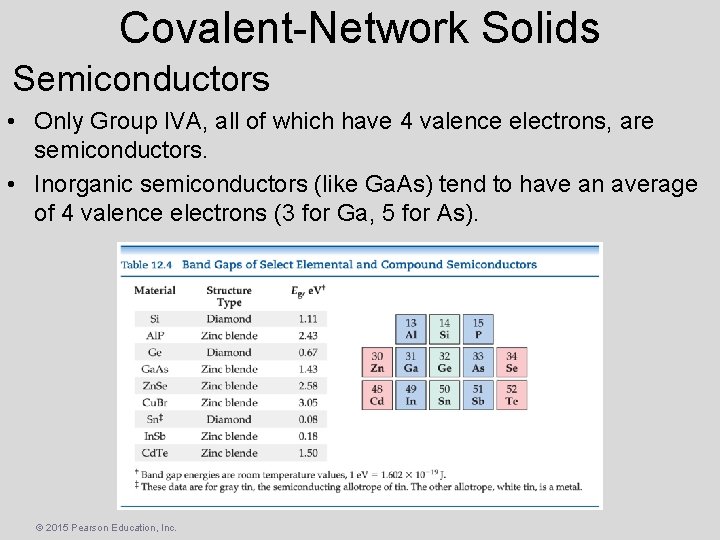
Covalent-Network Solids Semiconductors • Only Group IVA, all of which have 4 valence electrons, are semiconductors. • Inorganic semiconductors (like Ga. As) tend to have an average of 4 valence electrons (3 for Ga, 5 for As). © 2015 Pearson Education, Inc.

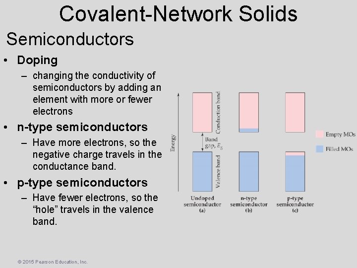
Covalent-Network Solids Semiconductors • Doping – changing the conductivity of semiconductors by adding an element with more or fewer electrons • n-type semiconductors – Have more electrons, so the negative charge travels in the conductance band. • p-type semiconductors – Have fewer electrons, so the “hole” travels in the valence band. © 2015 Pearson Education, Inc.

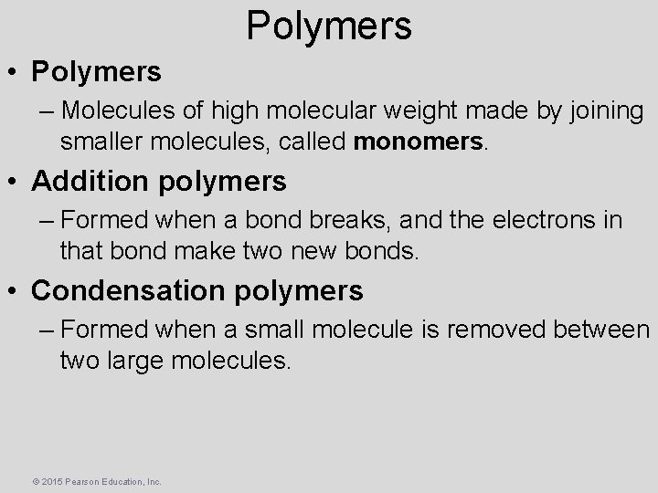
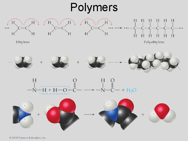
Polymers • Polymers – Molecules of high molecular weight made by joining smaller molecules, called monomers. • Addition polymers – Formed when a bond breaks, and the electrons in that bond make two new bonds. • Condensation polymers – Formed when a small molecule is removed between two large molecules. © 2015 Pearson Education, Inc.

Polymers © 2015 Pearson Education, Inc.

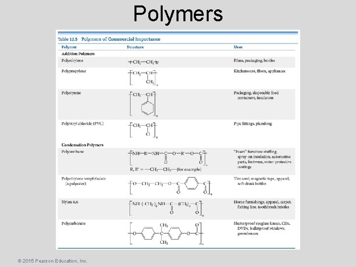
Polymers © 2015 Pearson Education, Inc.

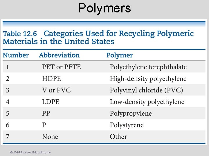
Polymers © 2015 Pearson Education, Inc.

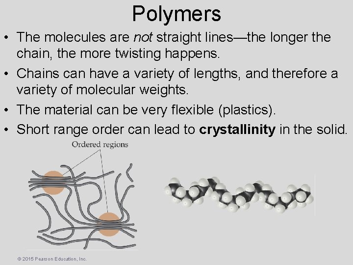
Polymers • The molecules are not straight lines—the longer the chain, the more twisting happens. • Chains can have a variety of lengths, and therefore a variety of molecular weights. • The material can be very flexible (plastics). • Short range order can lead to crystallinity in the solid. © 2015 Pearson Education, Inc.

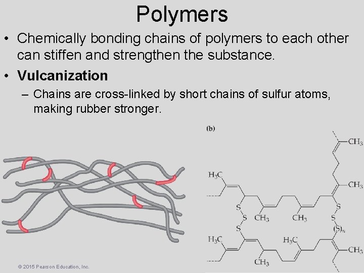
Polymers • Chemically bonding chains of polymers to each other can stiffen and strengthen the substance. • Vulcanization – Chains are cross-linked by short chains of sulfur atoms, making rubber stronger. © 2015 Pearson Education, Inc.

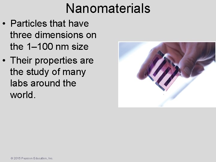
Nanomaterials • Particles that have three dimensions on the 1– 100 nm size • Their properties are the study of many labs around the world. © 2015 Pearson Education, Inc.

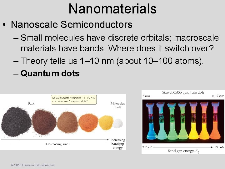
Nanomaterials • Nanoscale Semiconductors – Small molecules have discrete orbitals; macroscale materials have bands. Where does it switch over? – Theory tells us 1– 10 nm (about 10– 100 atoms). – Quantum dots © 2015 Pearson Education, Inc.

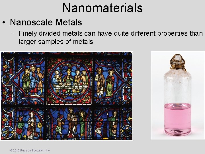
Nanomaterials • Nanoscale Metals – Finely divided metals can have quite different properties than larger samples of metals. © 2015 Pearson Education, Inc.

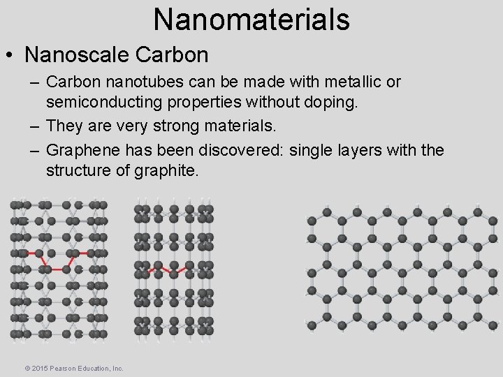
Nanomaterials • Nanoscale Carbon – Carbon nanotubes can be made with metallic or semiconducting properties without doping. – They are very strong materials. – Graphene has been discovered: single layers with the structure of graphite. © 2015 Pearson Education, Inc.