Intro to Microarchitecture SingleCycle CS 3330 Samira Khan






![Stage Computation: immovq irmovq V, r. B Fetch icode: ifun M 1[PC] Read instruction Stage Computation: immovq irmovq V, r. B Fetch icode: ifun M 1[PC] Read instruction](https://slidetodoc.com/presentation_image_h2/624d43f6ad99701aad1b50005a80fe56/image-74.jpg)

![Stage Computation: rrmovq r. A, r. B Fetch icode: ifun M 1[PC] Read instruction Stage Computation: rrmovq r. A, r. B Fetch icode: ifun M 1[PC] Read instruction](https://slidetodoc.com/presentation_image_h2/624d43f6ad99701aad1b50005a80fe56/image-84.jpg)


- Slides: 90

Intro to Microarchitecture: Single-Cycle CS 3330 Samira Khan University of Virginia Feb 9, 2017

AGENDA • Review from last lecture • ISA tradeoffs • Single-cycle Microarchitecture 2

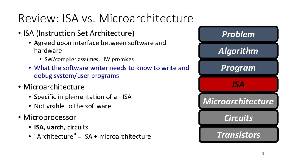
Review: ISA vs. Microarchitecture • ISA (Instruction Set Architecture) • Agreed upon interface between software and hardware • SW/compiler assumes, HW promises • What the software writer needs to know to write and debug system/user programs • Microarchitecture • Specific implementation of an ISA • Not visible to the software • Microprocessor • ISA, uarch, circuits • “Architecture” = ISA + microarchitecture Problem Algorithm Program ISA Microarchitecture Circuits Transistors 3

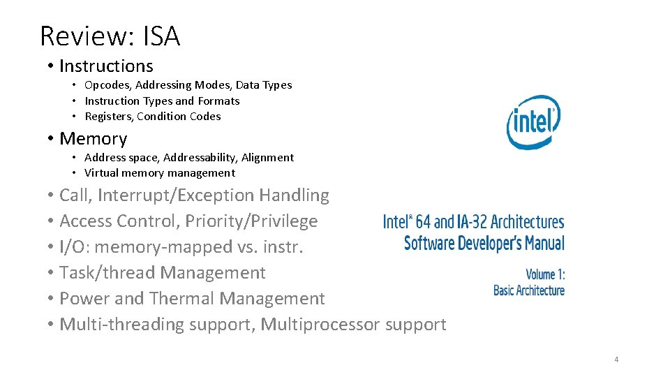
Review: ISA • Instructions • Opcodes, Addressing Modes, Data Types • Instruction Types and Formats • Registers, Condition Codes • Memory • Address space, Addressability, Alignment • Virtual memory management • Call, Interrupt/Exception Handling • Access Control, Priority/Privilege • I/O: memory-mapped vs. instr. • Task/thread Management • Power and Thermal Management • Multi-threading support, Multiprocessor support 4

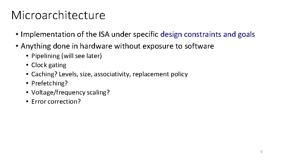
Microarchitecture • Implementation of the ISA under specific design constraints and goals • Anything done in hardware without exposure to software • • • Pipelining (will see later) Clock gating Caching? Levels, size, associativity, replacement policy Prefetching? Voltage/frequency scaling? Error correction? 5

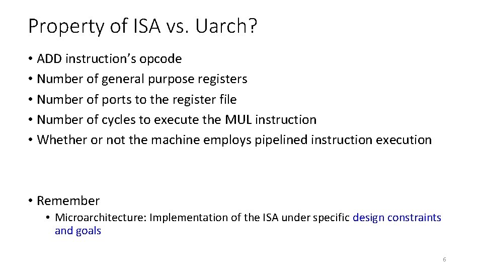
Property of ISA vs. Uarch? • ADD instruction’s opcode • Number of general purpose registers • Number of ports to the register file • Number of cycles to execute the MUL instruction • Whether or not the machine employs pipelined instruction execution • Remember • Microarchitecture: Implementation of the ISA under specific design constraints and goals 6

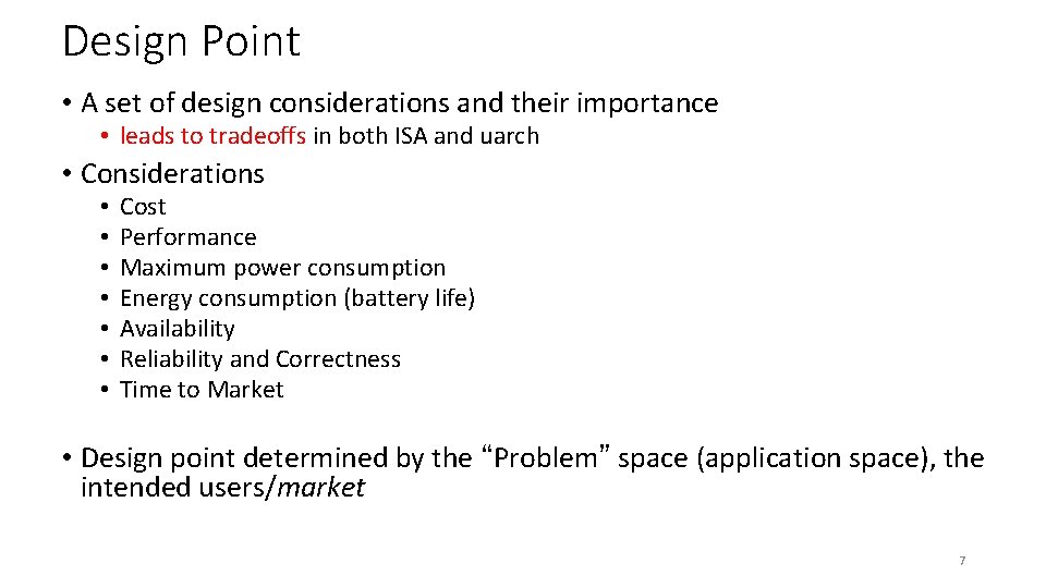
Design Point • A set of design considerations and their importance • leads to tradeoffs in both ISA and uarch • Considerations • • Cost Performance Maximum power consumption Energy consumption (battery life) Availability Reliability and Correctness Time to Market • Design point determined by the “Problem” space (application space), the intended users/market 7

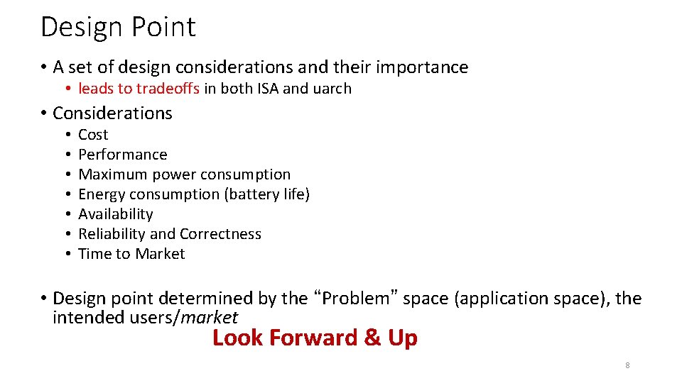
Design Point • A set of design considerations and their importance • leads to tradeoffs in both ISA and uarch • Considerations • • Cost Performance Maximum power consumption Energy consumption (battery life) Availability Reliability and Correctness Time to Market • Design point determined by the “Problem” space (application space), the intended users/market Look Forward & Up 8

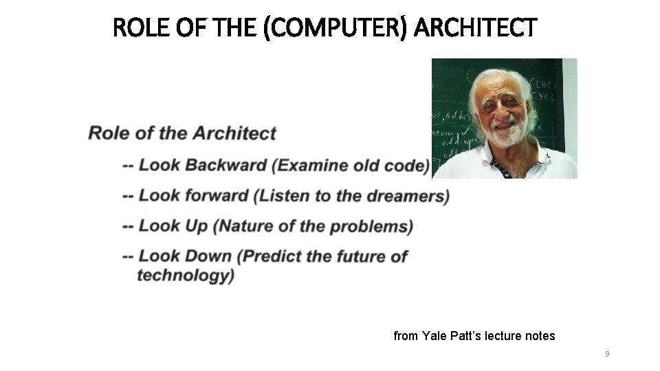
ROLE OF THE (COMPUTER) ARCHITECT from Yale Patt’s lecture notes 9

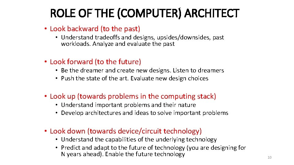
ROLE OF THE (COMPUTER) ARCHITECT • Look backward (to the past) • Understand tradeoffs and designs, upsides/downsides, past workloads. Analyze and evaluate the past • Look forward (to the future) • Be the dreamer and create new designs. Listen to dreamers • Push the state of the art. Evaluate new design choices • Look up (towards problems in the computing stack) • Understand important problems and their nature • Develop architectures and ideas to solve important problems • Look down (towards device/circuit technology) • Understand the capabilities of the underlying technology • Predict and adapt to the future of technology (you are designing for N years ahead). Enable the future technology 10

Application Space • Dream, and they will appear… 11

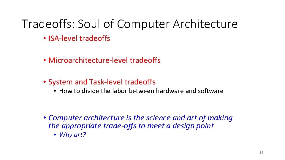
Tradeoffs: Soul of Computer Architecture • ISA-level tradeoffs • Microarchitecture-level tradeoffs • System and Task-level tradeoffs • How to divide the labor between hardware and software • Computer architecture is the science and art of making the appropriate trade-offs to meet a design point • Why art? 12

ISA Principles and Tradeoffs

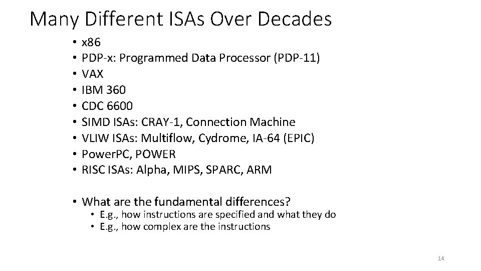
Many Different ISAs Over Decades • • • x 86 PDP-x: Programmed Data Processor (PDP-11) VAX IBM 360 CDC 6600 SIMD ISAs: CRAY-1, Connection Machine VLIW ISAs: Multiflow, Cydrome, IA-64 (EPIC) Power. PC, POWER RISC ISAs: Alpha, MIPS, SPARC, ARM • What are the fundamental differences? • E. g. , how instructions are specified and what they do • E. g. , how complex are the instructions 14

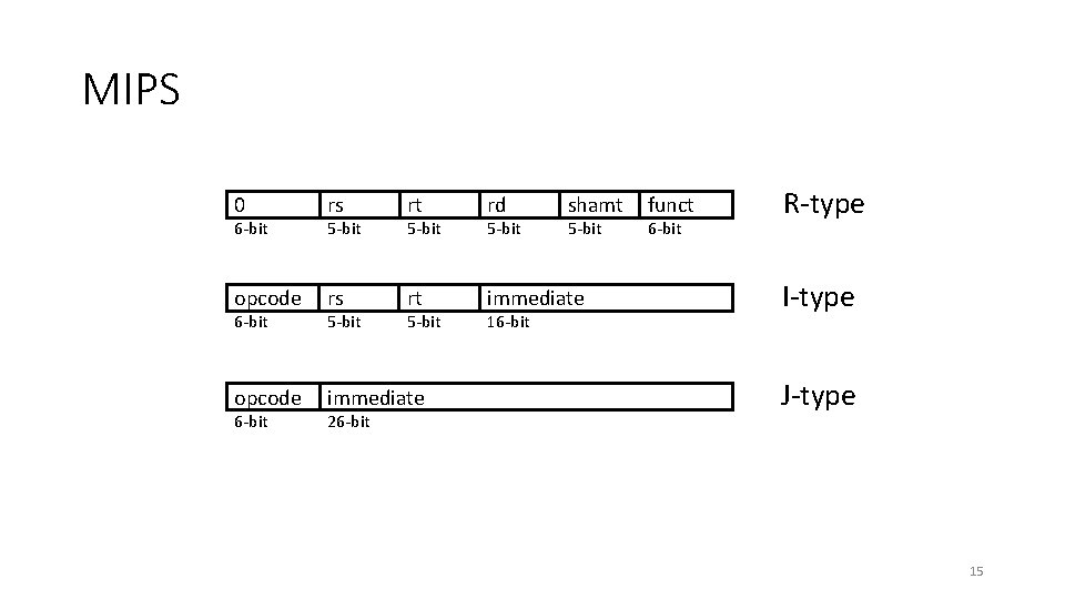
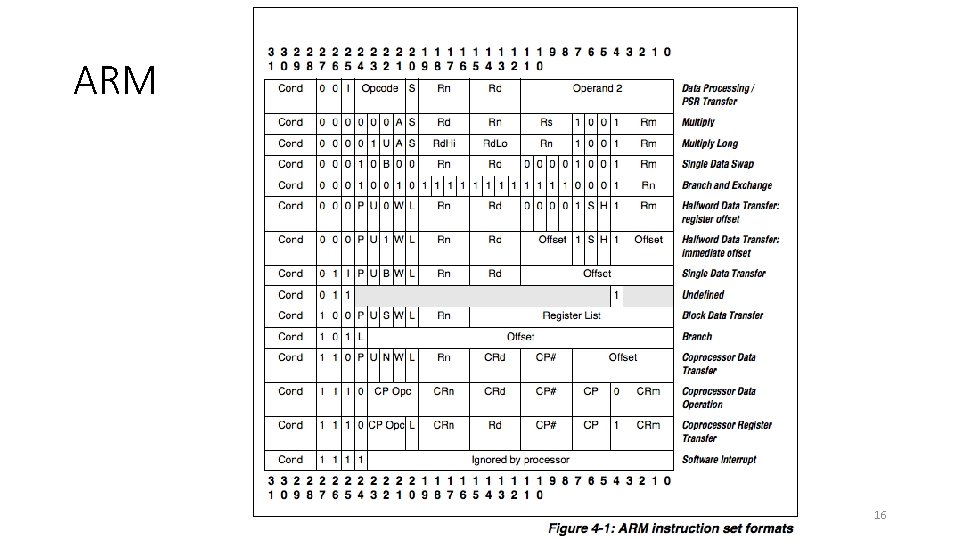
MIPS 0 rs rt rd opcode rs rt immediate opcode immediate 6 -bit 5 -bit 26 -bit 5 -bit 16 -bit shamt 5 -bit funct 6 -bit R-type I-type J-type 15

ARM 16

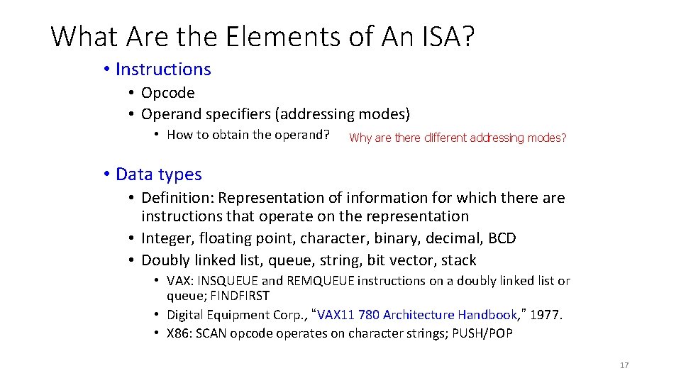
What Are the Elements of An ISA? • Instructions • Opcode • Operand specifiers (addressing modes) • How to obtain the operand? Why are there different addressing modes? • Data types • Definition: Representation of information for which there are instructions that operate on the representation • Integer, floating point, character, binary, decimal, BCD • Doubly linked list, queue, string, bit vector, stack • VAX: INSQUEUE and REMQUEUE instructions on a doubly linked list or queue; FINDFIRST • Digital Equipment Corp. , “VAX 11 780 Architecture Handbook, ” 1977. • X 86: SCAN opcode operates on character strings; PUSH/POP 17

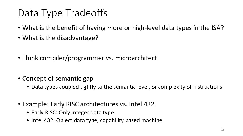
Data Type Tradeoffs • What is the benefit of having more or high-level data types in the ISA? • What is the disadvantage? • Think compiler/programmer vs. microarchitect • Concept of semantic gap • Data types coupled tightly to the semantic level, or complexity of instructions • Example: Early RISC architectures vs. Intel 432 • Early RISC: Only integer data type • Intel 432: Object data type, capability based machine 18

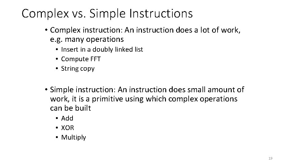
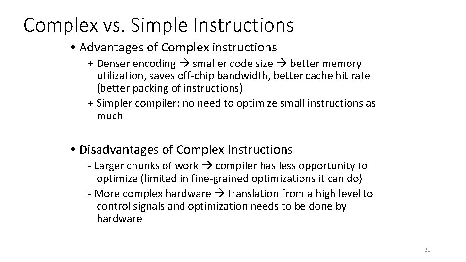
Complex vs. Simple Instructions • Complex instruction: An instruction does a lot of work, e. g. many operations • Insert in a doubly linked list • Compute FFT • String copy • Simple instruction: An instruction does small amount of work, it is a primitive using which complex operations can be built • Add • XOR • Multiply 19

Complex vs. Simple Instructions • Advantages of Complex instructions + Denser encoding smaller code size better memory utilization, saves off-chip bandwidth, better cache hit rate (better packing of instructions) + Simpler compiler: no need to optimize small instructions as much • Disadvantages of Complex Instructions - Larger chunks of work compiler has less opportunity to optimize (limited in fine-grained optimizations it can do) - More complex hardware translation from a high level to control signals and optimization needs to be done by hardware 20

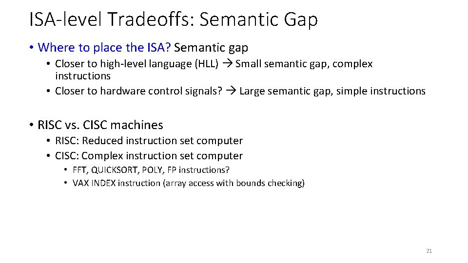
ISA-level Tradeoffs: Semantic Gap • Where to place the ISA? Semantic gap • Closer to high-level language (HLL) Small semantic gap, complex instructions • Closer to hardware control signals? Large semantic gap, simple instructions • RISC vs. CISC machines • RISC: Reduced instruction set computer • CISC: Complex instruction set computer • FFT, QUICKSORT, POLY, FP instructions? • VAX INDEX instruction (array access with bounds checking) 21

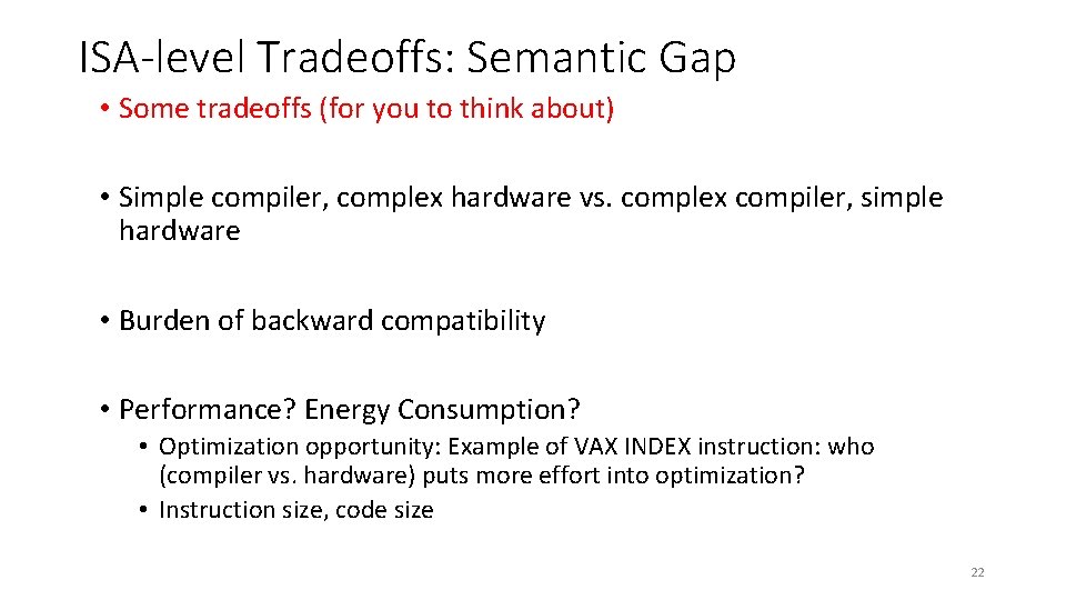
ISA-level Tradeoffs: Semantic Gap • Some tradeoffs (for you to think about) • Simple compiler, complex hardware vs. complex compiler, simple hardware • Burden of backward compatibility • Performance? Energy Consumption? • Optimization opportunity: Example of VAX INDEX instruction: who (compiler vs. hardware) puts more effort into optimization? • Instruction size, code size 22

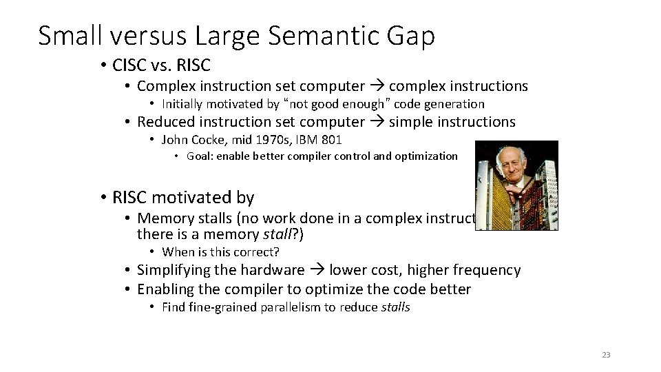
Small versus Large Semantic Gap • CISC vs. RISC • Complex instruction set computer complex instructions • Initially motivated by “not good enough” code generation • Reduced instruction set computer simple instructions • John Cocke, mid 1970 s, IBM 801 • Goal: enable better compiler control and optimization • RISC motivated by • Memory stalls (no work done in a complex instruction when there is a memory stall? ) • When is this correct? • Simplifying the hardware lower cost, higher frequency • Enabling the compiler to optimize the code better • Find fine-grained parallelism to reduce stalls 23

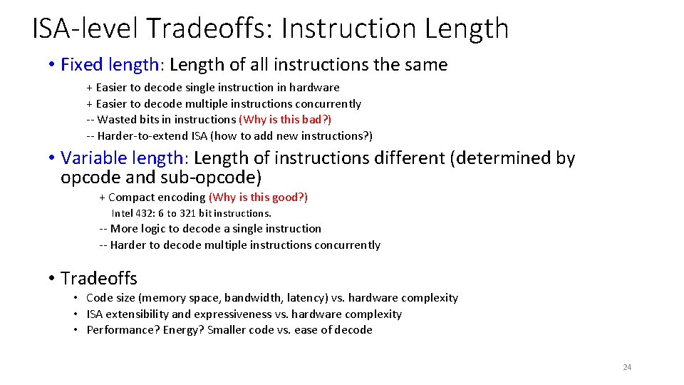
ISA-level Tradeoffs: Instruction Length • Fixed length: Length of all instructions the same + Easier to decode single instruction in hardware + Easier to decode multiple instructions concurrently -- Wasted bits in instructions (Why is this bad? ) -- Harder-to-extend ISA (how to add new instructions? ) • Variable length: Length of instructions different (determined by opcode and sub-opcode) + Compact encoding (Why is this good? ) Intel 432: 6 to 321 bit instructions. -- More logic to decode a single instruction -- Harder to decode multiple instructions concurrently • Tradeoffs • Code size (memory space, bandwidth, latency) vs. hardware complexity • ISA extensibility and expressiveness vs. hardware complexity • Performance? Energy? Smaller code vs. ease of decode 24

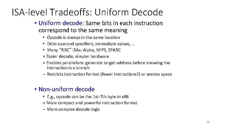
ISA-level Tradeoffs: Uniform Decode • Uniform decode: Same bits in each instruction correspond to the same meaning • Opcode is always in the same location • Ditto operand specifiers, immediate values, … • Many “RISC” ISAs: Alpha, MIPS, SPARC + Easier decode, simpler hardware + Enables parallelism: generate target address before knowing the instruction is a branch -- Restricts instruction format (fewer instructions? ) or wastes space • Non-uniform decode • E. g. , opcode can be the 1 st-7 th byte in x 86 + More compact and powerful instruction format -- More complex decode logic 25

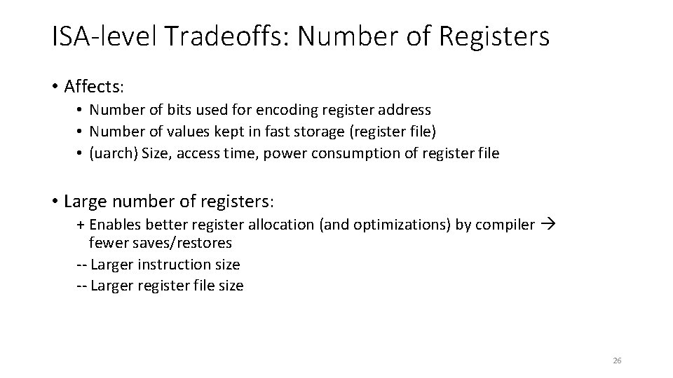
ISA-level Tradeoffs: Number of Registers • Affects: • Number of bits used for encoding register address • Number of values kept in fast storage (register file) • (uarch) Size, access time, power consumption of register file • Large number of registers: + Enables better register allocation (and optimizations) by compiler fewer saves/restores -- Larger instruction size -- Larger register file size 26

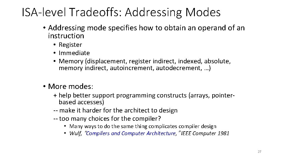
ISA-level Tradeoffs: Addressing Modes • Addressing mode specifies how to obtain an operand of an instruction • Register • Immediate • Memory (displacement, register indirect, indexed, absolute, memory indirect, autoincrement, autodecrement, …) • More modes: + help better support programming constructs (arrays, pointerbased accesses) -- make it harder for the architect to design -- too many choices for the compiler? • Many ways to do the same thing complicates compiler design • Wulf, “Compilers and Computer Architecture, ” IEEE Computer 1981 27

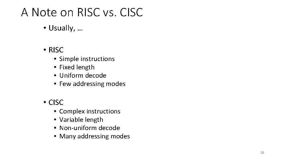
A Note on RISC vs. CISC • Usually, … • RISC • • Simple instructions Fixed length Uniform decode Few addressing modes • CISC • • Complex instructions Variable length Non-uniform decode Many addressing modes 28

Food for Thought for You • How would you design a new ISA? • Where would you place it? • What design choices would you make in terms of ISA properties? • What would be the first question you ask in this process? • “What is my design point? ” Look Forward & Up 29

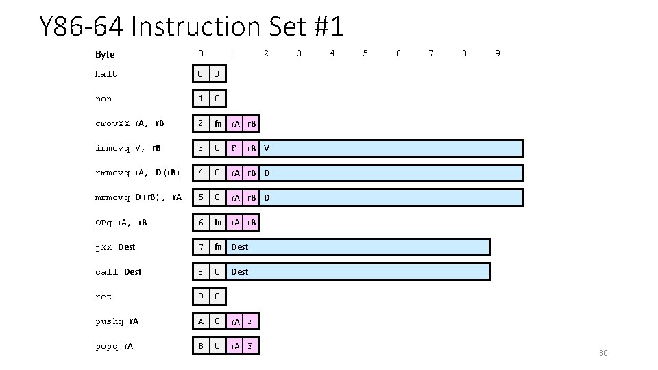
Y 86 -64 Instruction Set #1 Byte 0 halt 0 0 nop 1 0 cmov. XX r. A, r. B 2 fn r. A r. B irmovq V, r. B 3 0 F rmmovq r. A, D(r. B) 4 0 r. A r. B D mrmovq D(r. B), r. A 5 0 r. A r. B D OPq r. A, r. B 6 fn r. A r. B j. XX Dest 7 fn Dest call Dest 8 0 ret 9 0 pushq r. A A 0 r. A F popq r. A B 0 r. A F 1 2 3 4 5 6 7 8 9 r. B V Dest 30

Now That We Have an ISA • How do we implement it? • i. e. , how do we design a system that obeys the hardware/software interface? 31

Implementing the ISA: Microarchitecture Basics

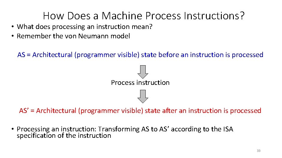
How Does a Machine Process Instructions? • What does processing an instruction mean? • Remember the von Neumann model AS = Architectural (programmer visible) state before an instruction is processed Process instruction AS’ = Architectural (programmer visible) state after an instruction is processed • Processing an instruction: Transforming AS to AS’ according to the ISA specification of the instruction 33

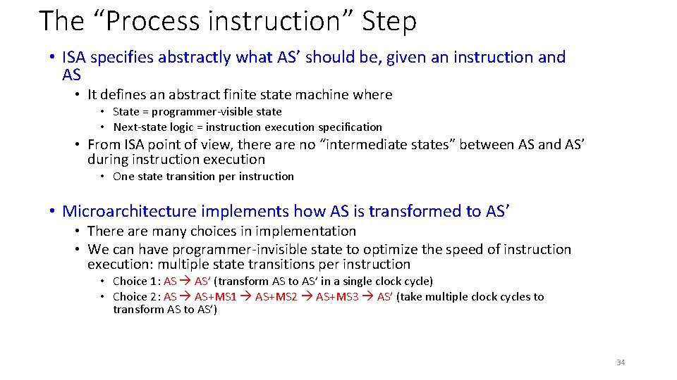
The “Process instruction” Step • ISA specifies abstractly what AS’ should be, given an instruction and AS • It defines an abstract finite state machine where • State = programmer-visible state • Next-state logic = instruction execution specification • From ISA point of view, there are no “intermediate states” between AS and AS’ during instruction execution • One state transition per instruction • Microarchitecture implements how AS is transformed to AS’ • There are many choices in implementation • We can have programmer-invisible state to optimize the speed of instruction execution: multiple state transitions per instruction • Choice 1: AS AS’ (transform AS to AS’ in a single clock cycle) • Choice 2: AS AS+MS 1 AS+MS 2 AS+MS 3 AS’ (take multiple clock cycles to transform AS to AS’) 34

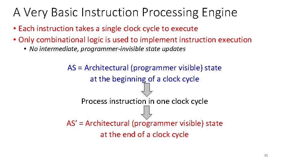
A Very Basic Instruction Processing Engine • Each instruction takes a single clock cycle to execute • Only combinational logic is used to implement instruction execution • No intermediate, programmer-invisible state updates AS = Architectural (programmer visible) state at the beginning of a clock cycle Process instruction in one clock cycle AS’ = Architectural (programmer visible) state at the end of a clock cycle 35

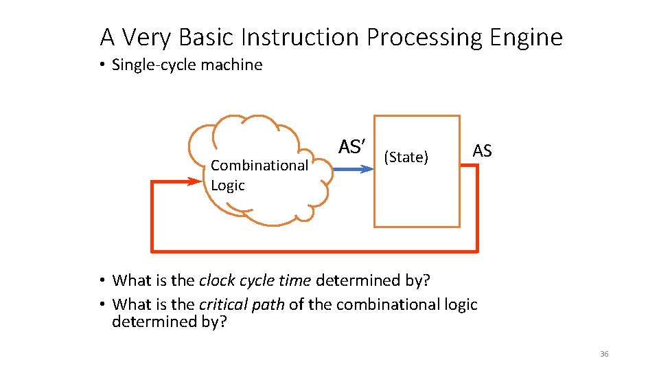
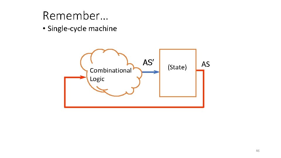
A Very Basic Instruction Processing Engine • Single-cycle machine Combinational Logic AS’ (State) AS • What is the clock cycle time determined by? • What is the critical path of the combinational logic determined by? 36

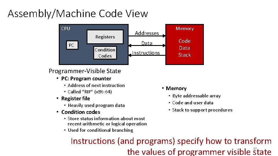
Assembly/Machine Code View CPU Registers PC Condition Codes Addresses Data Instructions Memory Code Data Stack Programmer-Visible State • PC: Program counter • Address of next instruction • Called “RIP” (x 86 -64) • Register file • Heavily used program data • Condition codes • Memory • Byte addressable array • Code and user data • Stack to support procedures • Store status information about most recent arithmetic or logical operation • Used for conditional branching Instructions (and programs) specify how to transform the values of programmer visible state 37

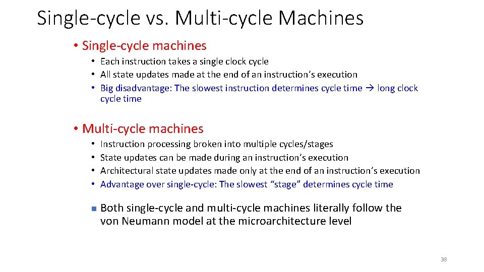
Single-cycle vs. Multi-cycle Machines • Single-cycle machines • Each instruction takes a single clock cycle • All state updates made at the end of an instruction’s execution • Big disadvantage: The slowest instruction determines cycle time long clock cycle time • Multi-cycle machines • • n Instruction processing broken into multiple cycles/stages State updates can be made during an instruction’s execution Architectural state updates made only at the end of an instruction’s execution Advantage over single-cycle: The slowest “stage” determines cycle time Both single-cycle and multi-cycle machines literally follow the von Neumann model at the microarchitecture level 38

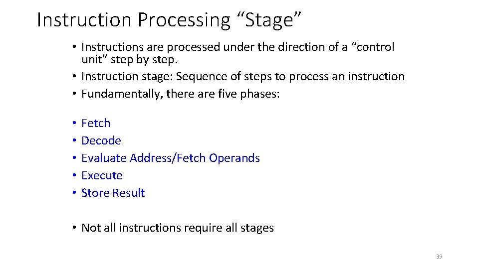
Instruction Processing “Stage” • Instructions are processed under the direction of a “control unit” step by step. • Instruction stage: Sequence of steps to process an instruction • Fundamentally, there are five phases: • • • Fetch Decode Evaluate Address/Fetch Operands Execute Store Result • Not all instructions require all stages 39

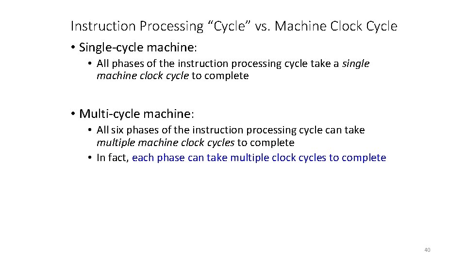
Instruction Processing “Cycle” vs. Machine Clock Cycle • Single-cycle machine: • All phases of the instruction processing cycle take a single machine clock cycle to complete • Multi-cycle machine: • All six phases of the instruction processing cycle can take multiple machine clock cycles to complete • In fact, each phase can take multiple clock cycles to complete 40

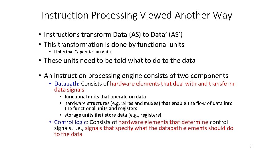
Instruction Processing Viewed Another Way • Instructions transform Data (AS) to Data’ (AS’) • This transformation is done by functional units • Units that “operate” on data • These units need to be told what to do to the data • An instruction processing engine consists of two components • Datapath: Consists of hardware elements that deal with and transform data signals • functional units that operate on data • hardware structures (e. g. wires and muxes) that enable the flow of data into the functional units and registers • storage units that store data (e. g. , registers) • Control logic: Consists of hardware elements that determine control signals, i. e. , signals that specify what the datapath elements should do to the data 41

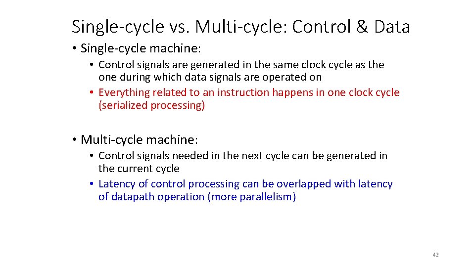
Single-cycle vs. Multi-cycle: Control & Data • Single-cycle machine: • Control signals are generated in the same clock cycle as the one during which data signals are operated on • Everything related to an instruction happens in one clock cycle (serialized processing) • Multi-cycle machine: • Control signals needed in the next cycle can be generated in the current cycle • Latency of control processing can be overlapped with latency of datapath operation (more parallelism) 42

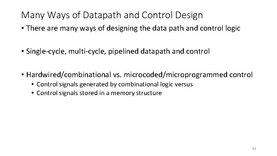
Many Ways of Datapath and Control Design • There are many ways of designing the data path and control logic • Single-cycle, multi-cycle, pipelined datapath and control • Hardwired/combinational vs. microcoded/microprogrammed control • Control signals generated by combinational logic versus • Control signals stored in a memory structure 43

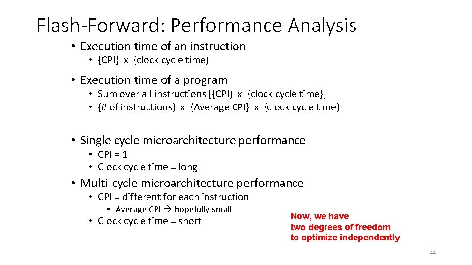
Flash-Forward: Performance Analysis • Execution time of an instruction • {CPI} x {clock cycle time} • Execution time of a program • Sum over all instructions [{CPI} x {clock cycle time}] • {# of instructions} x {Average CPI} x {clock cycle time} • Single cycle microarchitecture performance • CPI = 1 • Clock cycle time = long • Multi-cycle microarchitecture performance • CPI = different for each instruction • Average CPI hopefully small • Clock cycle time = short Now, we have two degrees of freedom to optimize independently 44

A Single-Cycle Microarchitecture A Closer Look

Remember… • Single-cycle machine Combinational Logic AS’ (State) AS 46

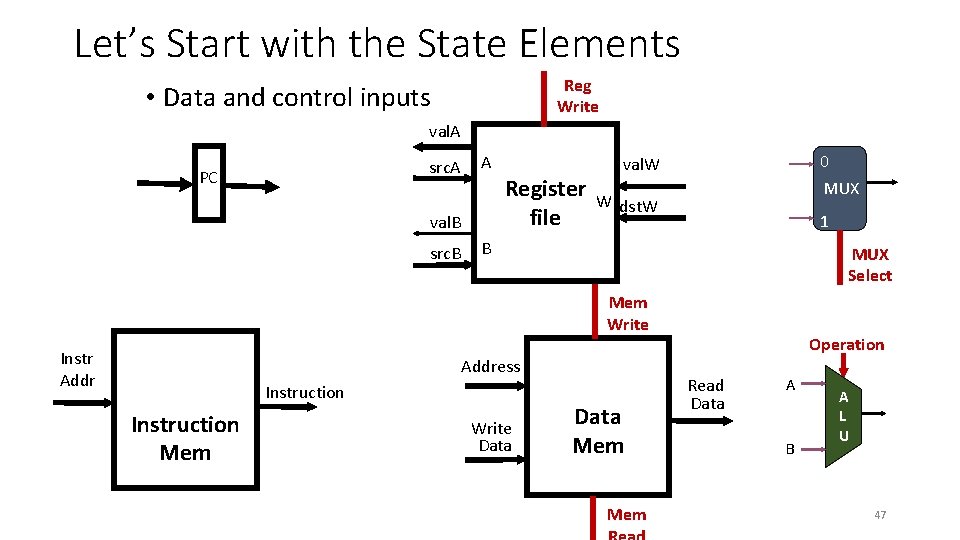
Let’s Start with the State Elements Reg Write • Data and control inputs val. A src. A PC A Register file val. B src. B 0 val. W MUX W dst. W 1 B MUX Select Mem Write Instr Address Instruction Mem Write Data Mem Operation Read Data A B A L U 47

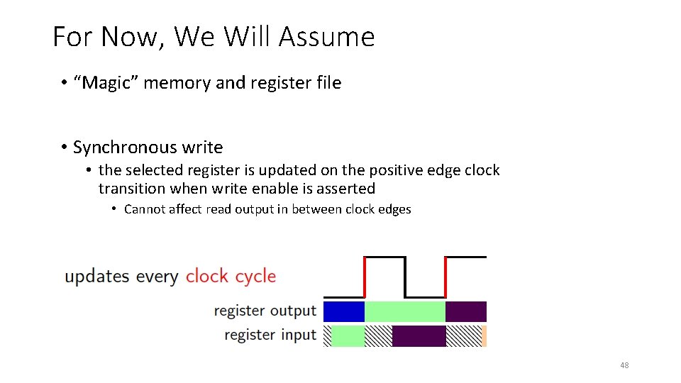
For Now, We Will Assume • “Magic” memory and register file • Synchronous write • the selected register is updated on the positive edge clock transition when write enable is asserted • Cannot affect read output in between clock edges 48

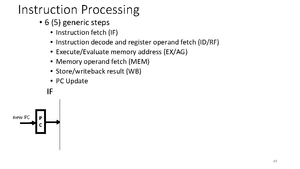
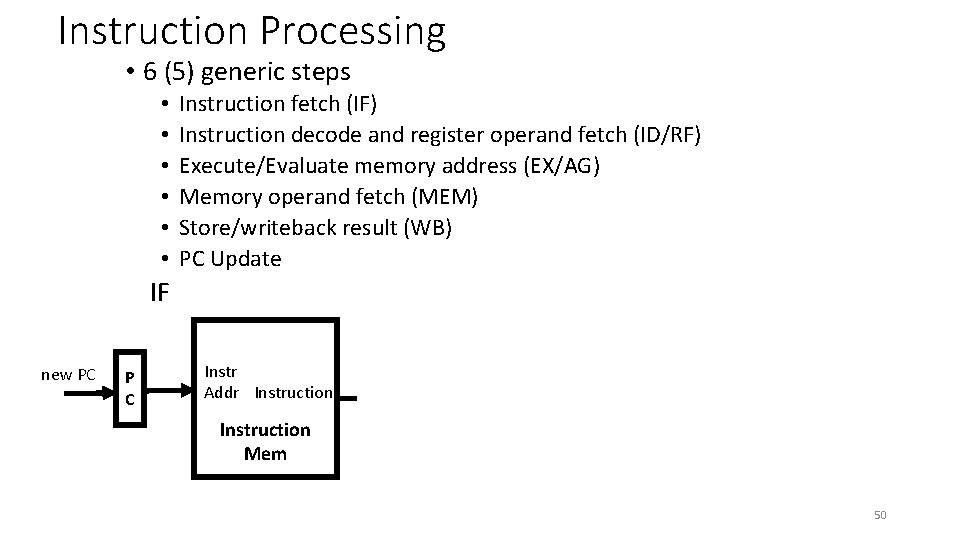
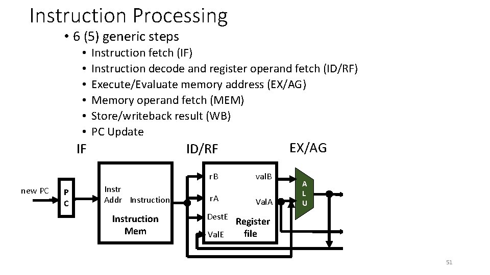
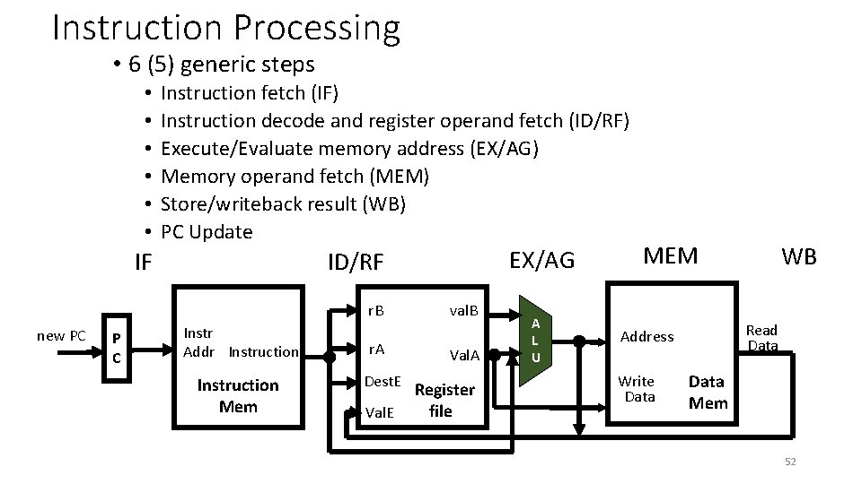
Instruction Processing • 6 (5) generic steps • • • Instruction fetch (IF) Instruction decode and register operand fetch (ID/RF) Execute/Evaluate memory address (EX/AG) Memory operand fetch (MEM) Store/writeback result (WB) PC Update IF EX/AG ID/RF r. B new PC P C Instr Addr Instruction Mem r. A Dest. E Val. E val. B Val. A Register file A L U MEM Read Data Address Write Data WB Data Mem 49

Instruction Processing • 6 (5) generic steps • • • Instruction fetch (IF) Instruction decode and register operand fetch (ID/RF) Execute/Evaluate memory address (EX/AG) Memory operand fetch (MEM) Store/writeback result (WB) PC Update IF r. B new PC P C EX/AG ID/RF Instr Addr Instruction Mem r. A Dest. E Val. E val. B Val. A Register file A L U MEM Read Data Address Write Data WB Data Mem 50

Instruction Processing • 6 (5) generic steps • • • Instruction fetch (IF) Instruction decode and register operand fetch (ID/RF) Execute/Evaluate memory address (EX/AG) Memory operand fetch (MEM) Store/writeback result (WB) PC Update IF r. B new PC P C EX/AG ID/RF Instr Addr Instruction Mem r. A Dest. E Val. E val. B Val. A Register file A L U MEM Read Data Address Write Data WB Data Mem 51

Instruction Processing • 6 (5) generic steps • • • Instruction fetch (IF) Instruction decode and register operand fetch (ID/RF) Execute/Evaluate memory address (EX/AG) Memory operand fetch (MEM) Store/writeback result (WB) PC Update IF r. B new PC P C EX/AG ID/RF Instr Addr Instruction Mem r. A Dest. E Val. E val. B Val. A Register file A L U MEM Read Data Address Write Data WB Data Mem 52

Single-Cycle Datapath for Arithmetic and Logical Instructions

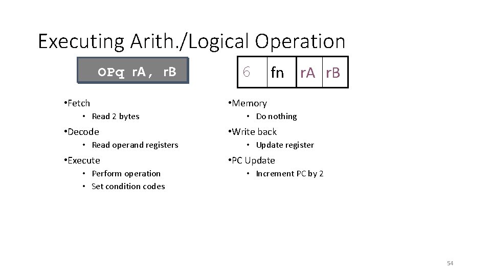
Executing Arith. /Logical Operation OPq r. A, r. B • Fetch • Read 2 bytes • Decode • Read operand registers • Execute • Perform operation • Set condition codes 6 fn r. A r. B • Memory • Do nothing • Write back • Update register • PC Update • Increment PC by 2 54

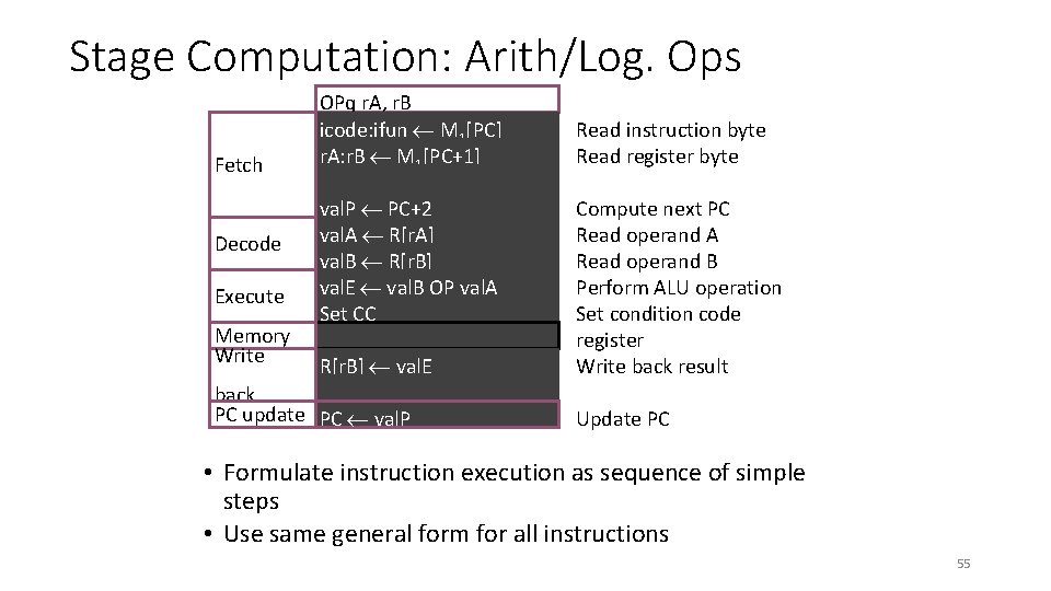
Stage Computation: Arith/Log. Ops Fetch Decode Execute Memory Write OPq r. A, r. B icode: ifun M 1[PC] r. A: r. B M 1[PC+1] val. P PC+2 val. A R[r. A] val. B R[r. B] val. E val. B OP val. A Set CC R[r. B] val. E back PC update PC val. P Read instruction byte Read register byte Compute next PC Read operand A Read operand B Perform ALU operation Set condition code register Write back result Update PC • Formulate instruction execution as sequence of simple steps • Use same general form for all instructions 55

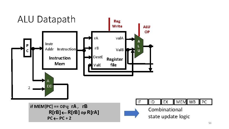
ALU Datapath Reg Write r. A P C Instr Addr Instruction Mem 2 r. B Dest. E Val. E val. A Val. B ALU OP A L U Read Data Address Register file Write Data Mem EX MEM WB A DD if MEM[PC] == OPq r. A, r. B R[r. B] op R[r. A] PC + 2 **Based on original figure from [P&H CO&D, COPYRIGHT 2004 Elsevier. ALL RIGHTS RESERVED. ] IF ID PC Combinational state update logic 56

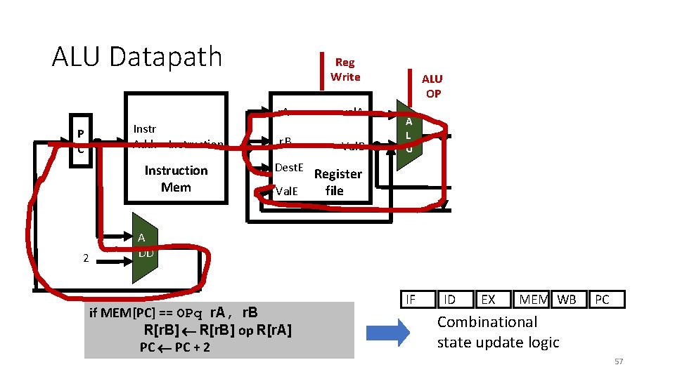
ALU Datapath Reg Write r. A P C Instr Addr Instruction Mem 2 r. B Dest. E Val. E val. A Val. B ALU OP A L U Read Data Address Register file Write Data Mem EX MEM WB A DD if MEM[PC] == OPq r. A, r. B R[r. B] op R[r. A] PC + 2 **Based on original figure from [P&H CO&D, COPYRIGHT 2004 Elsevier. ALL RIGHTS RESERVED. ] IF ID PC Combinational state update logic 57

We did not cover these slides in the class Will learn about these in the next class They are here for your benefit

Single-Cycle Datapath for Data Movement Instructions

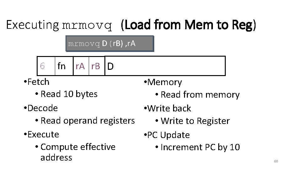
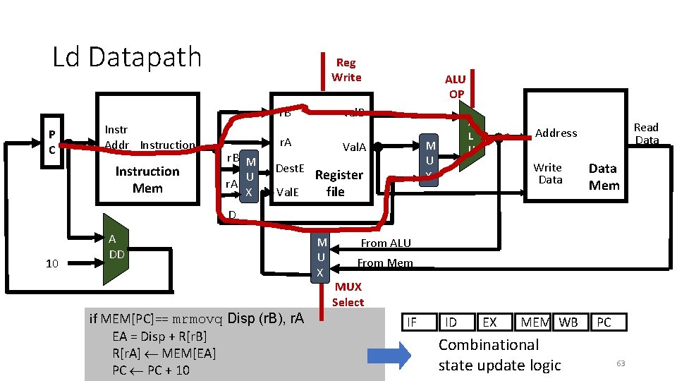
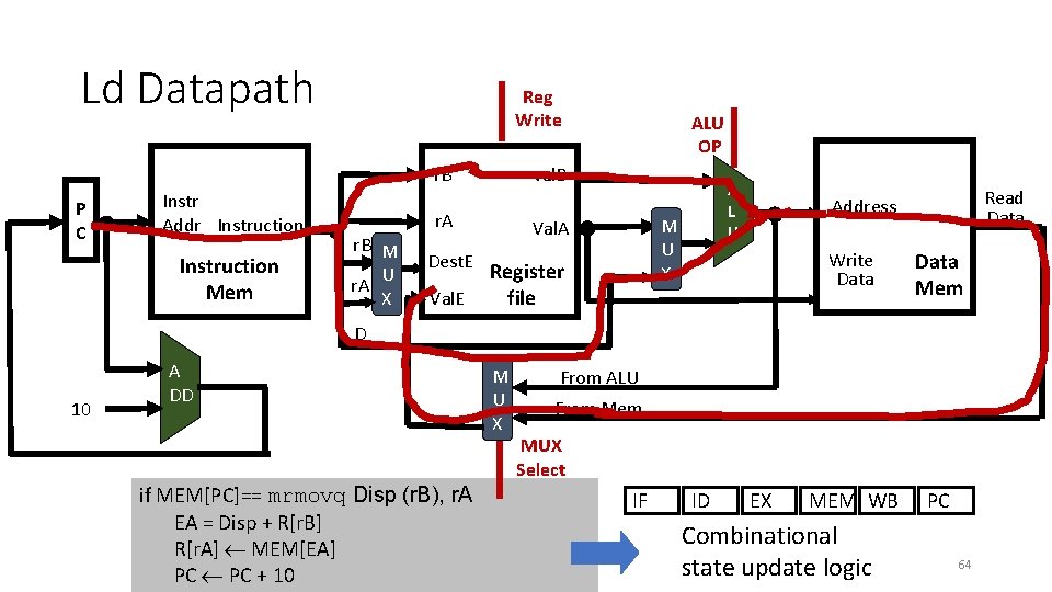
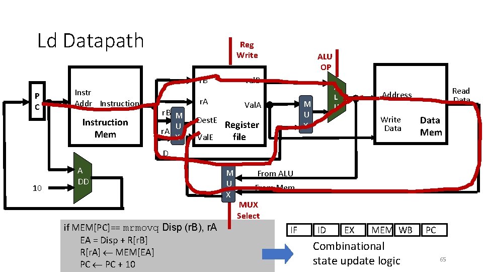
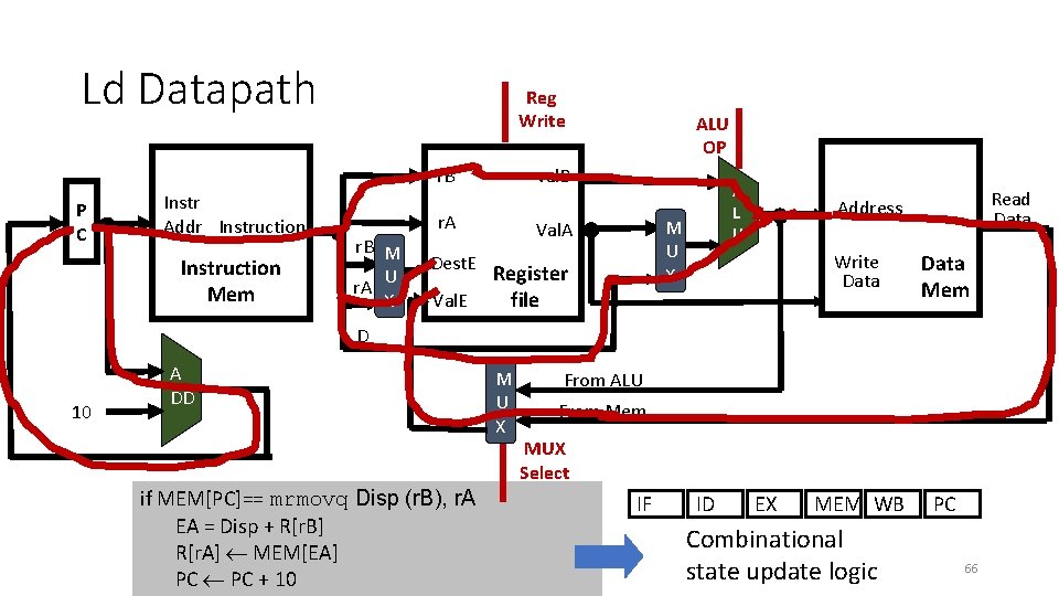
Executing mrmovq (Load from Mem to Reg) mrmovq D(r. B) , r. A 6 fn r. A r. B D • Fetch • Memory • Read 10 bytes • Read from memory • Decode • Write back • Read operand registers • Write to Register • Execute • PC Update • Compute effective • Increment PC by 10 address 60

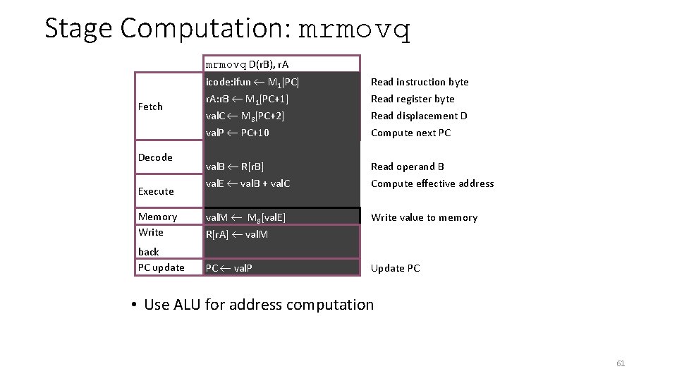
Stage Computation: mrmovq D(r. B), r. A Fetch Decode Execute Memory Write back PC update icode: ifun M 1[PC] Read instruction byte r. A: r. B M 1[PC+1] Read register byte val. C M 8[PC+2] Read displacement D val. P PC+10 Compute next PC val. B R[r. B] Read operand B val. E val. B + val. C Compute effective address val. M M 8[val. E] Write value to memory R[r. A] val. M PC val. P Update PC • Use ALU for address computation 61

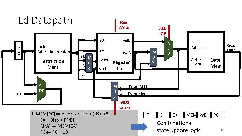
Ld Datapath Reg Write val. B r. B P C Instr Addr Instruction Mem r. B M U r. A X r. A Dest. E Val. E ALU OP A L U M U X Val. A Register file Read Data Address Write Data Mem MEM WB PC D 10 A DD if MEM[PC]== mrmovq Disp (r. B), r. A EA = Disp + R[r. B] R[r. A] MEM[EA] PC + 10 M U X From ALU From Mem MUX Select IF ID EX Combinational state update logic 62

Ld Datapath Reg Write val. B r. B P C Instr Addr Instruction Mem r. B M U r. A X r. A Dest. E Val. E ALU OP A L U M U X Val. A Register file Read Data Address Write Data Mem MEM WB PC D 10 A DD if MEM[PC]== mrmovq Disp (r. B), r. A EA = Disp + R[r. B] R[r. A] MEM[EA] PC + 10 M U X From ALU From Mem MUX Select IF ID EX Combinational state update logic 63

Ld Datapath Reg Write val. B r. B P C Instr Addr Instruction Mem r. B M U r. A X r. A Dest. E Val. E ALU OP A L U M U X Val. A Register file Read Data Address Write Data Mem MEM WB PC D 10 A DD if MEM[PC]== mrmovq Disp (r. B), r. A EA = Disp + R[r. B] R[r. A] MEM[EA] PC + 10 M U X From ALU From Mem MUX Select IF ID EX Combinational state update logic 64

Ld Datapath Reg Write val. B r. B P C Instr Addr Instruction Mem r. B M U r. A X r. A Dest. E Val. E ALU OP A L U M U X Val. A Register file Read Data Address Write Data Mem MEM WB PC D 10 A DD if MEM[PC]== mrmovq Disp (r. B), r. A EA = Disp + R[r. B] R[r. A] MEM[EA] PC + 10 M U X From ALU From Mem MUX Select IF ID EX Combinational state update logic 65

Ld Datapath Reg Write val. B r. B P C Instr Addr Instruction Mem r. B M U r. A X r. A Dest. E Val. E ALU OP A L U M U X Val. A Register file Read Data Address Write Data Mem MEM WB PC D 10 A DD if MEM[PC]== mrmovq Disp (r. B), r. A EA = Disp + R[r. B] R[r. A] MEM[EA] PC + 10 M U X From ALU From Mem MUX Select IF ID EX Combinational state update logic 66

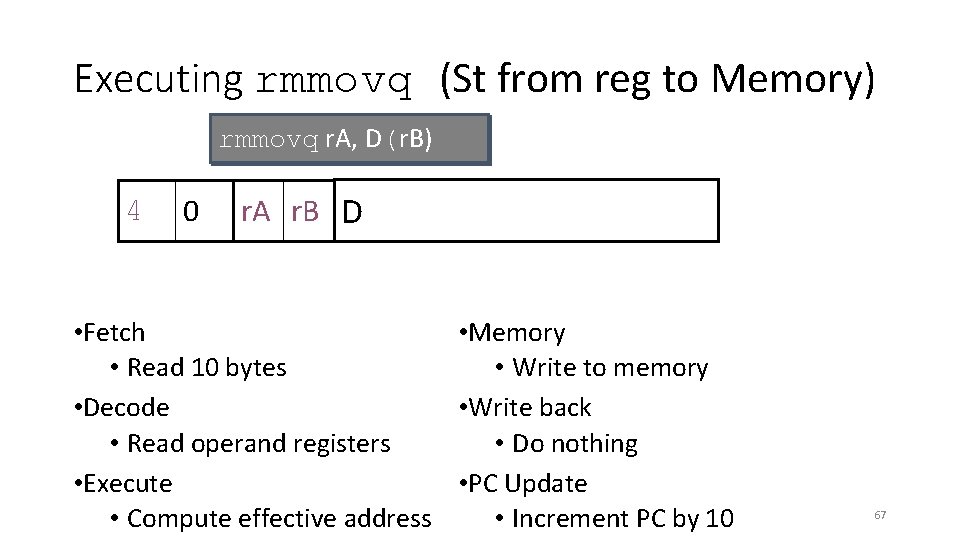
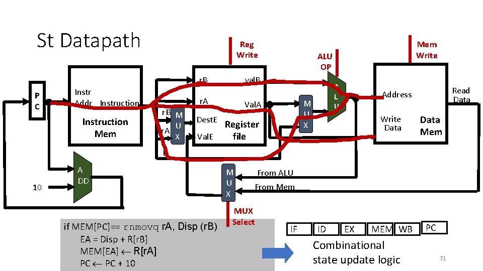
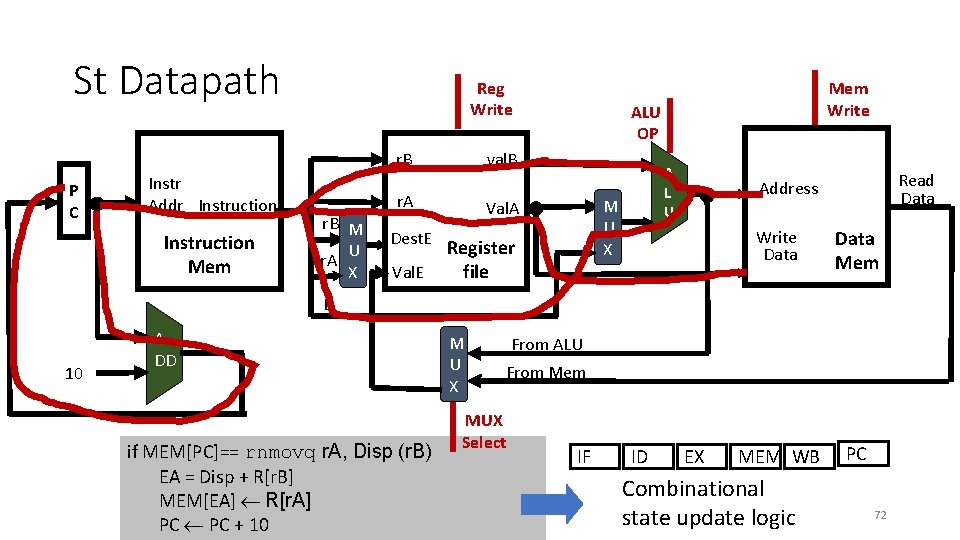
Executing rmmovq (St from reg to Memory) rmmovq r. A, D(r. B) 4 0 r. A r. B D • Fetch • Memory • Read 10 bytes • Write to memory • Decode • Write back • Read operand registers • Do nothing • Execute • PC Update • Compute effective address • Increment PC by 10 67

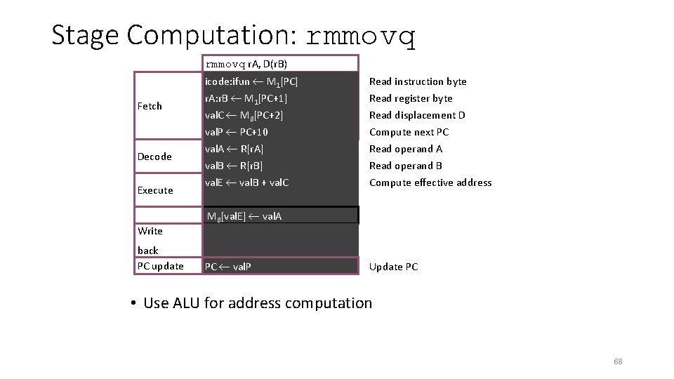
Stage Computation: rmmovq r. A, D(r. B) Fetch Decode Execute Memory Write back PC update icode: ifun M 1[PC] Read instruction byte r. A: r. B M 1[PC+1] Read register byte val. C M 8[PC+2] Read displacement D val. P PC+10 Compute next PC val. A R[r. A] Read operand A val. B R[r. B] Read operand B val. E val. B + val. C Compute effective address M 8[val. E] val. A Write value to memory PC val. P Update PC • Use ALU for address computation 68

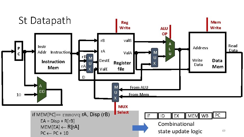
St Datapath Reg Write P C Instr Addr Instruction Mem r. B M U r. A X r. A Dest. E Val. E ALU OP val. B r. B Mem Write A L U M U X Val. A Register file Read Data Address Write Data Mem MEM WB PC D 10 A DD if MEM[PC]== rmmovq r. A, Disp (r. B) EA = Disp + R[r. B] MEM[EA] R[r. A] PC + 10 M U X From ALU From Mem MUX Select IF ID EX Combinational state update logic 69

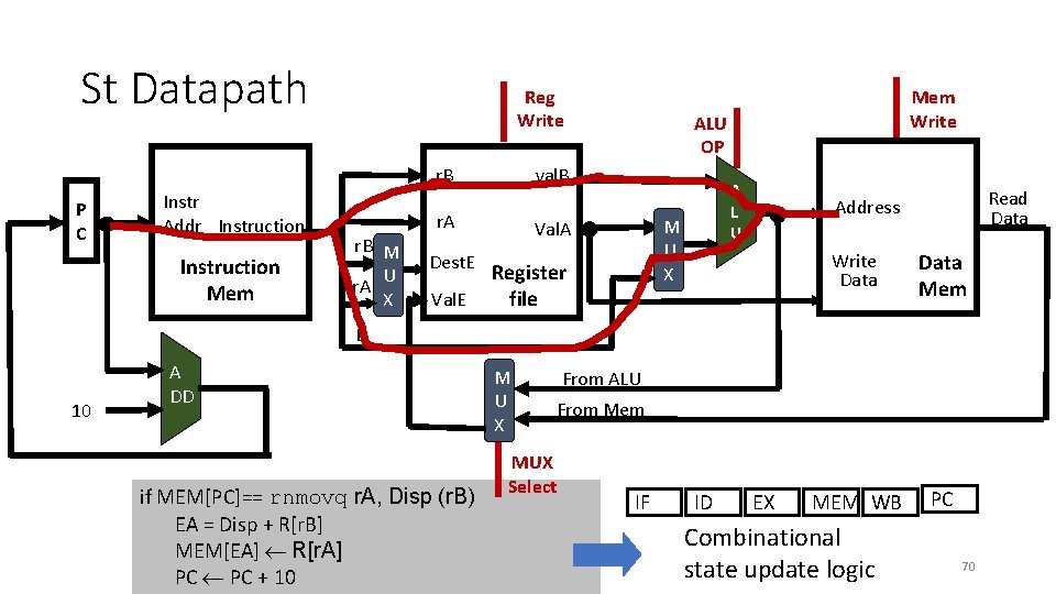
St Datapath Reg Write P C Instr Addr Instruction Mem r. B M U r. A X r. A Dest. E Val. E ALU OP val. B r. B Mem Write A L U M U X Val. A Register file Read Data Address Write Data Mem MEM WB PC D 10 A DD if MEM[PC]== rnmovq r. A, Disp (r. B) EA = Disp + R[r. B] MEM[EA] R[r. A] PC + 10 M U X From ALU From Mem MUX Select IF ID EX Combinational state update logic 70

St Datapath Reg Write P C Instr Addr Instruction Mem r. B M U r. A X r. A Dest. E Val. E ALU OP val. B r. B Mem Write A L U M U X Val. A Register file Read Data Address Write Data Mem MEM WB PC D 10 A DD if MEM[PC]== rnmovq r. A, Disp (r. B) EA = Disp + R[r. B] MEM[EA] R[r. A] PC + 10 M U X From ALU From Mem MUX Select IF ID EX Combinational state update logic 71

St Datapath Reg Write P C Instr Addr Instruction Mem r. B M U r. A X r. A Dest. E Val. E ALU OP val. B r. B Mem Write A L U M U X Val. A Register file Read Data Address Write Data Mem MEM WB PC D 10 A DD if MEM[PC]== rnmovq r. A, Disp (r. B) EA = Disp + R[r. B] MEM[EA] R[r. A] PC + 10 M U X From ALU From Mem MUX Select IF ID EX Combinational state update logic 72

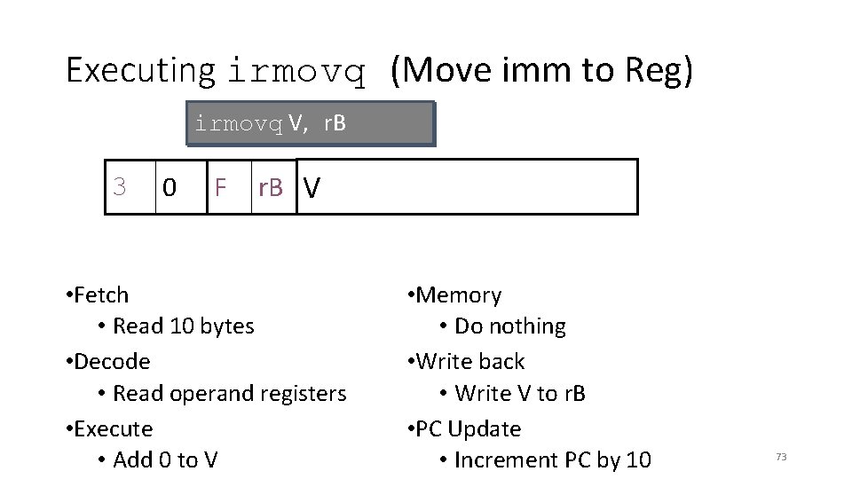
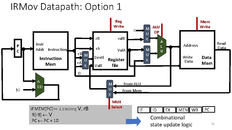
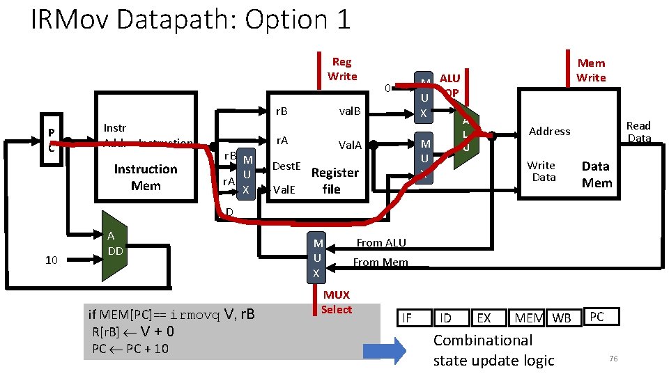
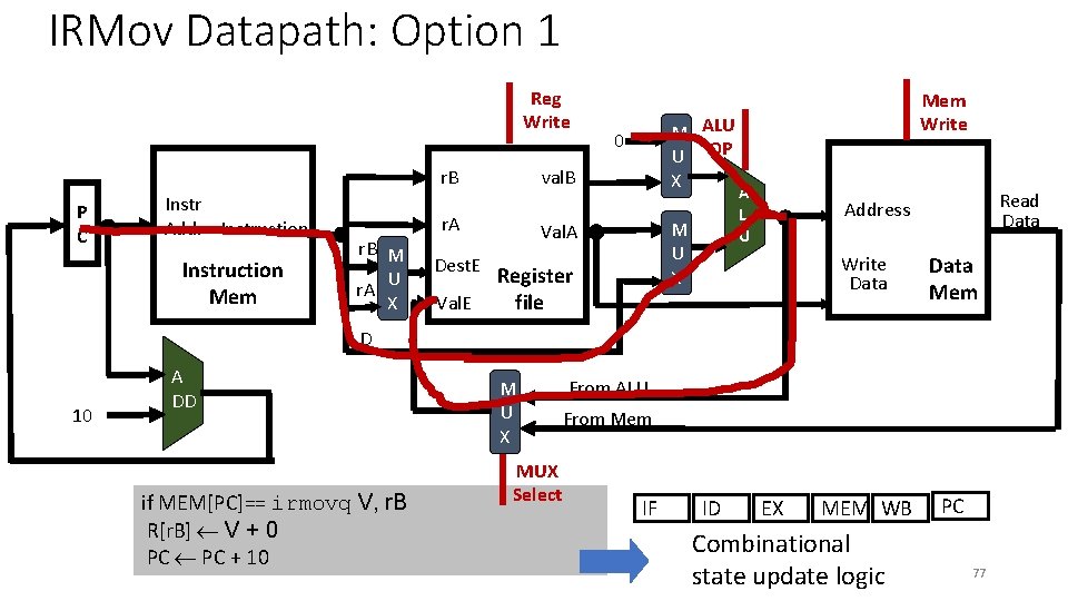
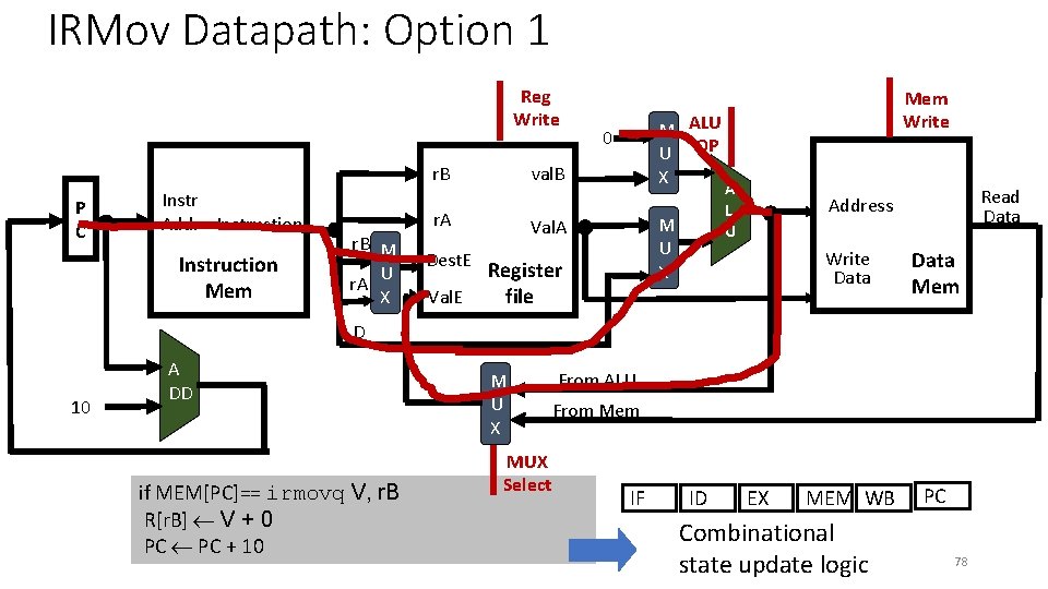
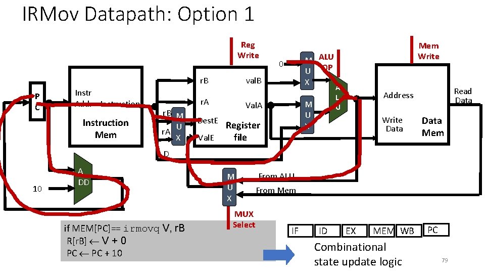
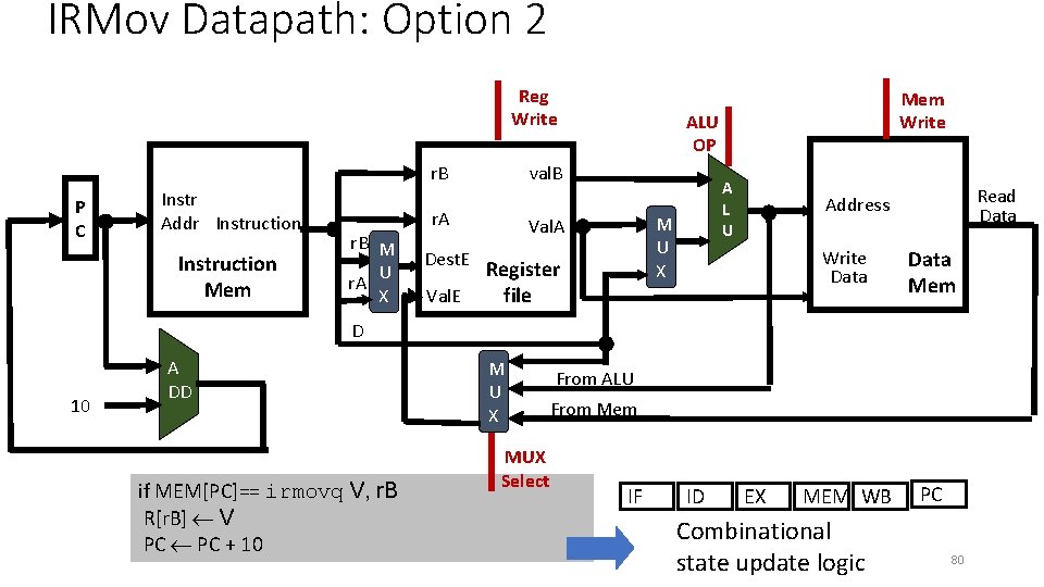
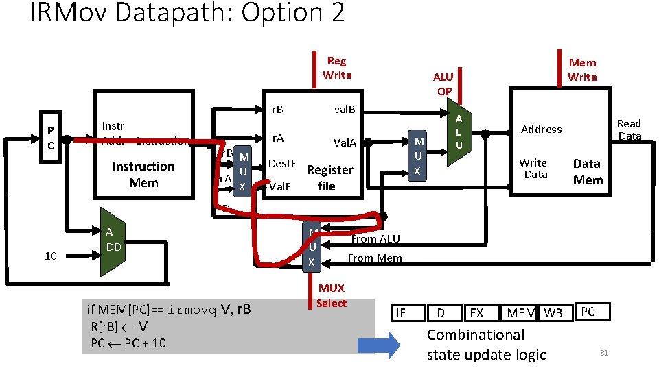
Executing irmovq (Move imm to Reg) irmovq V, r. B 3 0 F r. B V • Fetch • Read 10 bytes • Decode • Read operand registers • Execute • Add 0 to V • Memory • Do nothing • Write back • Write V to r. B • PC Update • Increment PC by 10 73
![Stage Computation immovq irmovq V r B Fetch icode ifun M 1PC Read instruction Stage Computation: immovq irmovq V, r. B Fetch icode: ifun M 1[PC] Read instruction](https://slidetodoc.com/presentation_image_h2/624d43f6ad99701aad1b50005a80fe56/image-74.jpg)
Stage Computation: immovq irmovq V, r. B Fetch icode: ifun M 1[PC] Read instruction byte r. A: r. B M 1[PC+1] Read register byte val. C M 8[PC+2] Read displacement D val. P PC+10 Compute next PC val. E 0 + val. C Compute effective address R[r. B] val. A Write value to memory PC val. P Update PC Decode Execute Memory Write back PC update • Use ALU for address computation 74

IRMov Datapath: Option 1 Reg Write val. B r. B P C Instr Addr Instruction Mem r. B M U r. A X r. A Dest. E Val. E M ALU U OP X 0 M U X Val. A Register file Mem Write A L U Read Data Address Write Data Mem MEM WB PC D 10 A DD if MEM[PC]== irmovq V, r. B R[r. B] V PC + 10 M U X MUX Select From ALU From Mem IF ID EX Combinational state update logic 75

IRMov Datapath: Option 1 Reg Write val. B r. B P C Instr Addr Instruction Mem r. B M U r. A X r. A Dest. E Val. E M ALU U OP X 0 M U X Val. A Register file Mem Write A L U Read Data Address Write Data Mem MEM WB PC D 10 A DD if MEM[PC]== irmovq V, r. B R[r. B] V + 0 PC + 10 M U X MUX Select From ALU From Mem IF ID EX Combinational state update logic 76

IRMov Datapath: Option 1 Reg Write val. B r. B P C Instr Addr Instruction Mem r. B M U r. A X r. A Dest. E Val. E M ALU U OP X 0 M U X Val. A Register file Mem Write A L U Read Data Address Write Data Mem MEM WB PC D 10 A DD if MEM[PC]== irmovq V, r. B R[r. B] V + 0 PC + 10 M U X MUX Select From ALU From Mem IF ID EX Combinational state update logic 77

IRMov Datapath: Option 1 Reg Write val. B r. B P C Instr Addr Instruction Mem r. B M U r. A X r. A Dest. E Val. E M ALU U OP X 0 M U X Val. A Register file Mem Write A L U Read Data Address Write Data Mem MEM WB PC D 10 A DD if MEM[PC]== irmovq V, r. B R[r. B] V + 0 PC + 10 M U X MUX Select From ALU From Mem IF ID EX Combinational state update logic 78

IRMov Datapath: Option 1 Reg Write val. B r. B P C Instr Addr Instruction Mem r. B M U r. A X r. A Dest. E Val. E M ALU U OP X 0 M U X Val. A Register file Mem Write A L U Read Data Address Write Data Mem MEM WB PC D 10 A DD if MEM[PC]== irmovq V, r. B R[r. B] V + 0 PC + 10 M U X MUX Select From ALU From Mem IF ID EX Combinational state update logic 79

IRMov Datapath: Option 2 Reg Write P C Instr Addr Instruction Mem r. B M U r. A X r. A Dest. E Val. E ALU OP val. B r. B Mem Write A L U M U X Val. A Register file Read Data Address Write Data Mem MEM WB PC D 10 A DD if MEM[PC]== irmovq V, r. B R[r. B] V PC + 10 M U X MUX Select From ALU From Mem IF ID EX Combinational state update logic 80

IRMov Datapath: Option 2 Reg Write P C Instr Addr Instruction Mem r. B M U r. A X r. A Dest. E Val. E ALU OP val. B r. B Mem Write A L U M U X Val. A Register file Read Data Address Write Data Mem MEM WB PC D 10 A DD if MEM[PC]== irmovq V, r. B R[r. B] V PC + 10 M U X MUX Select From ALU From Mem IF ID EX Combinational state update logic 81

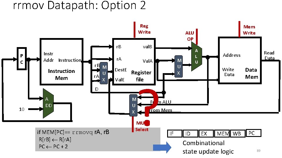
• Tradeoffs between option 1 and option 2? 82

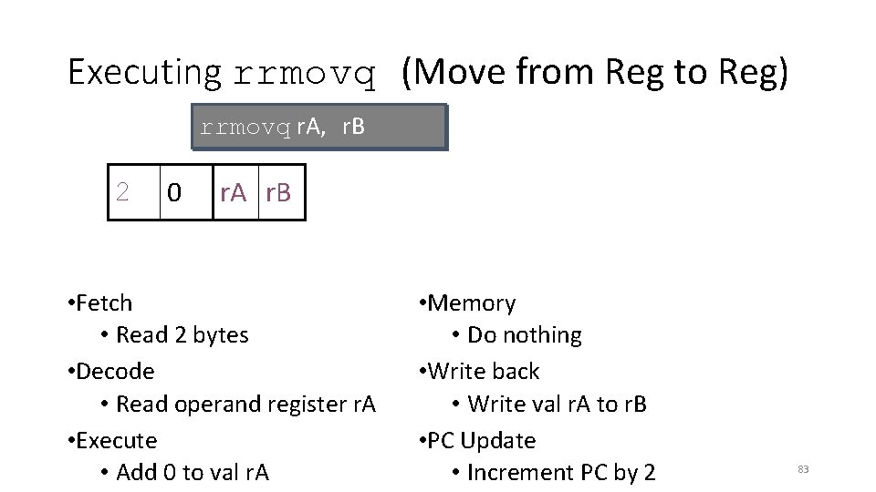
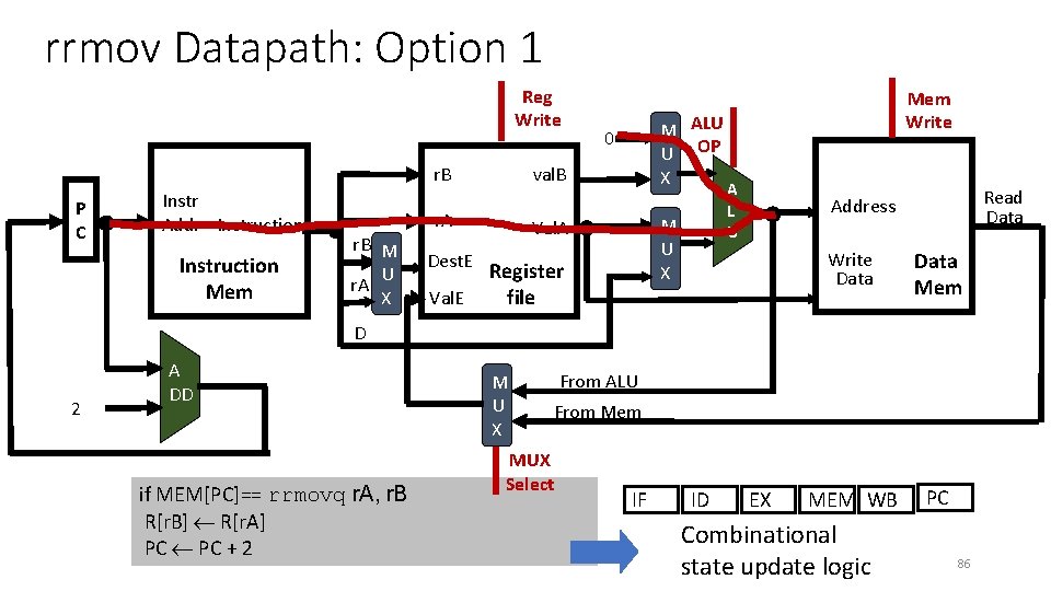
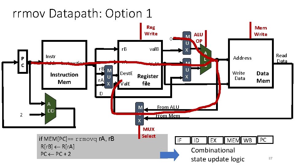
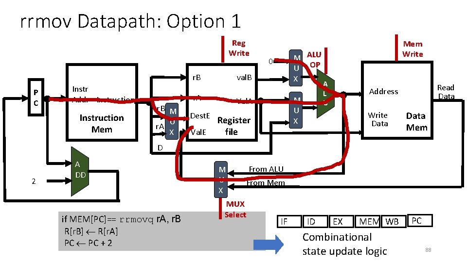
Executing rrmovq (Move from Reg to Reg) rrmovq r. A, r. B 2 0 r. A r. B • Fetch • Read 2 bytes • Decode • Read operand register r. A • Execute • Add 0 to val r. A • Memory • Do nothing • Write back • Write val r. A to r. B • PC Update • Increment PC by 2 83
![Stage Computation rrmovq r A r B Fetch icode ifun M 1PC Read instruction Stage Computation: rrmovq r. A, r. B Fetch icode: ifun M 1[PC] Read instruction](https://slidetodoc.com/presentation_image_h2/624d43f6ad99701aad1b50005a80fe56/image-84.jpg)
Stage Computation: rrmovq r. A, r. B Fetch icode: ifun M 1[PC] Read instruction byte r. A: r. B M 1[PC+1] Read register byte Read displacement D val. P PC+2 Decode Execute Compute next PC Val. A R[r. A] val. E 0 + val. A Memory Write R[r. B] val. E back PC update PC val. P Compute effective address Write value to memory Update PC • Use ALU for address computation 84

rr. Mov Datapath: Option 1 Reg Write val. B r. B P C Instr Addr Instruction Mem r. B M U r. A X r. A Dest. E Val. E M ALU U OP X 0 M U X Val. A Register file Mem Write A L U Read Data Address Write Data Mem MEM WB PC D 2 A DD if MEM[PC]== rrmovq r. A, r. B R[r. B] R[r. A] PC + 2 M U X From ALU From Mem MUX Select IF ID EX Combinational state update logic 85

rrmov Datapath: Option 1 Reg Write val. B r. B P C Instr Addr Instruction Mem r. B M U r. A X r. A Dest. E Val. E M ALU U OP X 0 M U X Val. A Register file Mem Write A L U Read Data Address Write Data Mem MEM WB PC D 2 A DD if MEM[PC]== rrmovq r. A, r. B R[r. B] R[r. A] PC + 2 M U X From ALU From Mem MUX Select IF ID EX Combinational state update logic 86

rrmov Datapath: Option 1 Reg Write val. B r. B P C Instr Addr Instruction Mem r. B M U r. A X r. A Dest. E Val. E M ALU U OP X 0 M U X Val. A Register file Mem Write A L U Read Data Address Write Data Mem MEM WB PC D 2 A DD if MEM[PC]== rrmovq r. A, r. B R[r. B] R[r. A] PC + 2 M U X From ALU From Mem MUX Select IF ID EX Combinational state update logic 87

rrmov Datapath: Option 1 Reg Write val. B r. B P C Instr Addr Instruction Mem r. B M U r. A X r. A Dest. E Val. E M ALU U OP X 0 M U X Val. A Register file Mem Write A L U Read Data Address Write Data Mem MEM WB PC D 2 A DD if MEM[PC]== rrmovq r. A, r. B R[r. B] R[r. A] PC + 2 M U X From ALU From Mem MUX Select IF ID EX Combinational state update logic 88

rrmov Datapath: Option 2 Reg Write P C Instr Addr Instruction Mem r. B M U r. A X D 10 A DD if MEM[PC]== rrmovq r. A, r. B R[r. B] R[r. A] PC + 2 r. A Dest. E Val. E ALU OP val. B r. B Register file ? MUX Select A L U M U X Val. A M U X Mem Write Read Data Address Write Data Mem MEM WB PC From ALU From Mem IF ID EX Combinational state update logic 89

Intro to Microarchitecture: Single-Cycle CS 3330 Samira Khan University of Virginia Feb 9, 2017