COMPUTER ARCHITECTURE CS 6354 Main Memory Samira Khan

- Slides: 53

COMPUTER ARCHITECTURE CS 6354 Main Memory Samira Khan University of Virginia Mar 3, 2016 The content and concept of this course are adapted from CMU ECE 740

AGENDA • Logistics • Review from last lecture • Main Memory 2

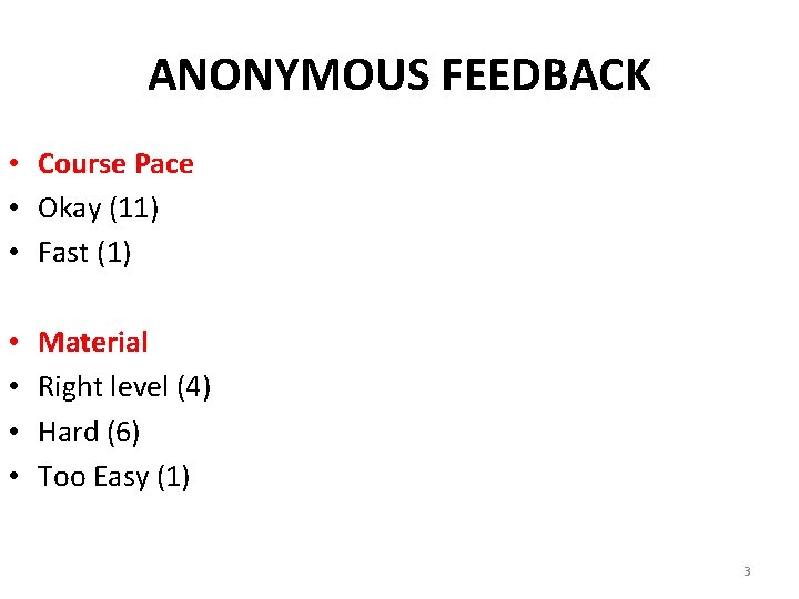
ANONYMOUS FEEDBACK • Course Pace • Okay (11) • Fast (1) • • Material Right level (4) Hard (6) Too Easy (1) 3

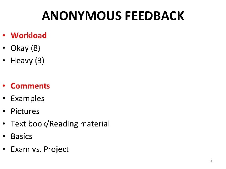
ANONYMOUS FEEDBACK • Workload • Okay (8) • Heavy (3) • • • Comments Examples Pictures Text book/Reading material Basics Exam vs. Project 4

MATERIAL • Undergraduate Computer Architecture Course – Includes more than what we are covering in this course • Watch the lecture videos • https: //www. youtube. com/watch? v=BJ 87 r. ZCGWU 0&l ist=PL 5 PHm 2 jkk. Xmid. JOd 59 REog 9 j. Dn. PDTG 6 IJ • https: //www. youtube. com/watch? v=z. LP_X 4 wy. Hb. Y&li st=PL 5 PHm 2 jkk. Xmi 5 Cxx. I 7 b 3 JCL 1 TWyb. TDt. Kq • Readings • http: //www. ece. cmu. edu/~ece 447/s 15/doku. php? id= readings 5

TEXTBOOK • Textbooks do not provide the high-level intuition behind the ideas • Many of the ideas are not yet in the text book – Want to learn state of the art, and their tradeoffs • Want to answer the question – Why? – What was done before? – Why this is better? – What are the downsides? …. But do consult the textbook if you need …. 6

EXAM VS. PROJECT VS. GRADE • Focus on project • Exams are just to make sure you understood the material • You want to learn the topics • Grades do not get you a job, acquired skill does • Your project shows – You know the recent topics – You know the tools – You can implement and evaluate ideas 7

REVIEW: USE OF ASYMMETRY FOR ENERGY EFFICIENCY • Kumar et al. , “Single-ISA Heterogeneous Multi-Core Architectures: The Potential for Processor Power Reduction, ” MICRO 2003. • Idea: – Implement multiple types of cores on chip – Monitor characteristics of the running thread (e. g. , sample energy/perf on each core periodically) – Dynamically pick the core that provides the best energy/performance tradeoff for a given phase • “Best core” Depends on optimization metric 8

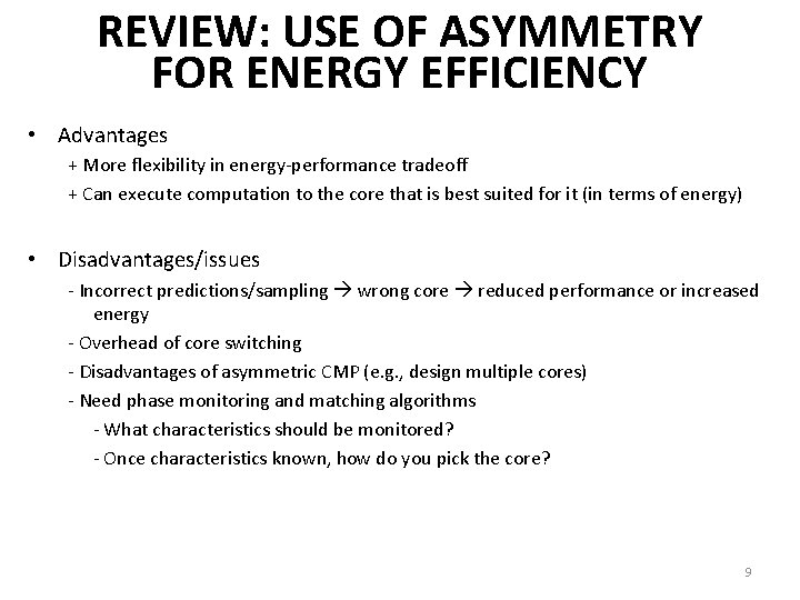
REVIEW: USE OF ASYMMETRY FOR ENERGY EFFICIENCY • Advantages + More flexibility in energy-performance tradeoff + Can execute computation to the core that is best suited for it (in terms of energy) • Disadvantages/issues - Incorrect predictions/sampling wrong core reduced performance or increased energy - Overhead of core switching - Disadvantages of asymmetric CMP (e. g. , design multiple cores) - Need phase monitoring and matching algorithms - What characteristics should be monitored? - Once characteristics known, how do you pick the core? 9

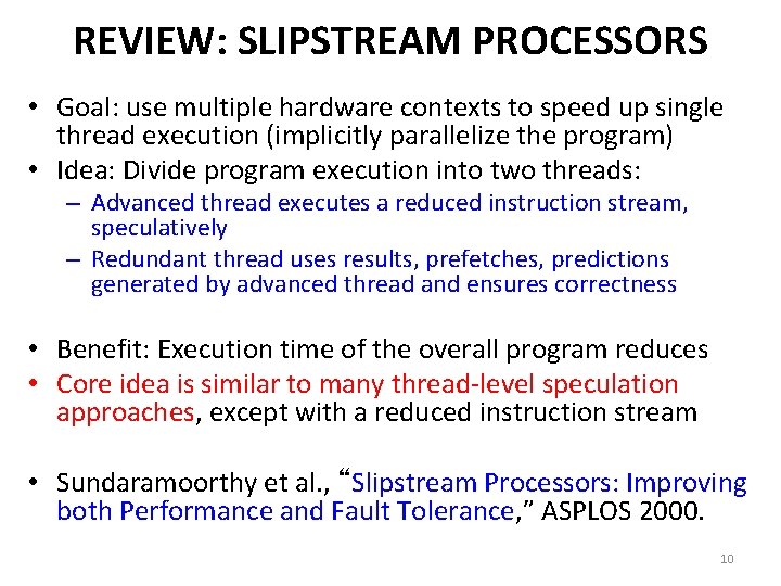
REVIEW: SLIPSTREAM PROCESSORS • Goal: use multiple hardware contexts to speed up single thread execution (implicitly parallelize the program) • Idea: Divide program execution into two threads: – Advanced thread executes a reduced instruction stream, speculatively – Redundant thread uses results, prefetches, predictions generated by advanced thread and ensures correctness • Benefit: Execution time of the overall program reduces • Core idea is similar to many thread-level speculation approaches, except with a reduced instruction stream • Sundaramoorthy et al. , “Slipstream Processors: Improving both Performance and Fault Tolerance, ” ASPLOS 2000. 10

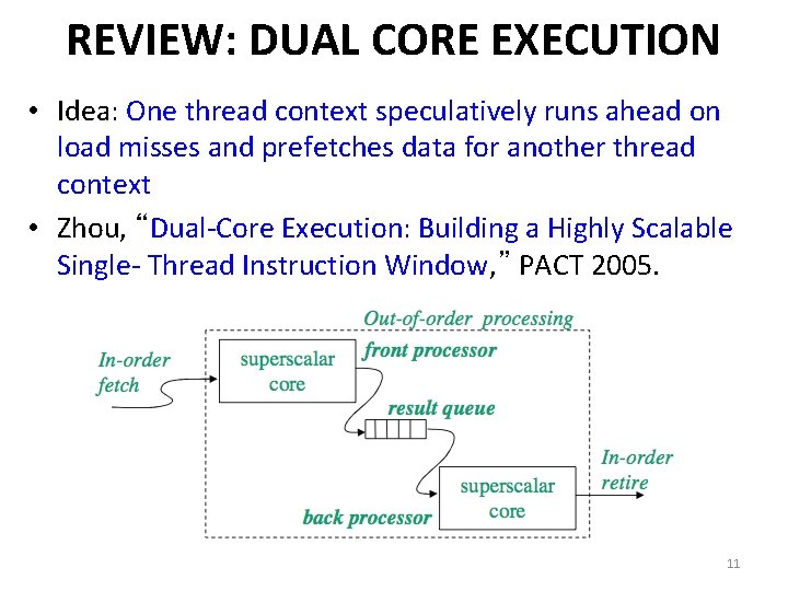
REVIEW: DUAL CORE EXECUTION • Idea: One thread context speculatively runs ahead on load misses and prefetches data for another thread context • Zhou, “Dual-Core Execution: Building a Highly Scalable Single- Thread Instruction Window, ” PACT 2005. 11

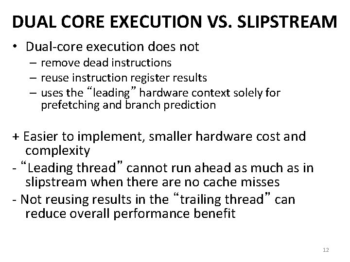
DUAL CORE EXECUTION VS. SLIPSTREAM • Dual-core execution does not – remove dead instructions – reuse instruction register results – uses the “leading” hardware context solely for prefetching and branch prediction + Easier to implement, smaller hardware cost and complexity - “Leading thread” cannot run ahead as much as in slipstream when there are no cache misses - Not reusing results in the “trailing thread” can reduce overall performance benefit 12

HETEROGENEITY (ASYMMETRY) SPECIALIZATION • Heterogeneity and asymmetry have the same meaning – Contrast with homogeneity and symmetry • Heterogeneity is a very general system design concept (and life concept, as well) • Idea: Instead of having multiple instances of the same “resource” to be the same (i. e. , homogeneous or symmetric), design some instances to be different (i. e. , heterogeneous or asymmetric) • Different instances can be optimized to be more efficient in executing different types of workloads or satisfying different requirements/goals – Heterogeneity enables specialization/customization 13

WHY ASYMMETRY IN DESIGN? (I) • Different workloads executing in a system can have different behavior – Different applications can have different behavior – Different execution phases of an application can have different behavior – The same application executing at different times can have different behavior (due to input set changes and dynamic events) – E. g. , locality, predictability of branches, instruction-level parallelism, data dependencies, serial fraction, bottlenecks in parallel portion, interference characteristics, … • Systems are designed to satisfy different metrics at the same time – There is almost never a single goal in design, depending on design point – E. g. , Performance, energy efficiency, fairness, predictability, reliability, availability, cost, memory capacity, latency, bandwidth, … 14

WHY ASYMMETRY IN DESIGN? (II) • Problem: Symmetric design is one-size-fits-all • It tries to fit a single-size design to all workloads and metrics • It is very difficult to come up with a single design – that satisfies all workloads even for a single metric – that satisfies all design metrics at the same time • This holds true for different system components, or resources – Cores, caches, memory, controllers, interconnect, disks, servers, … – Algorithms, policies, … 15

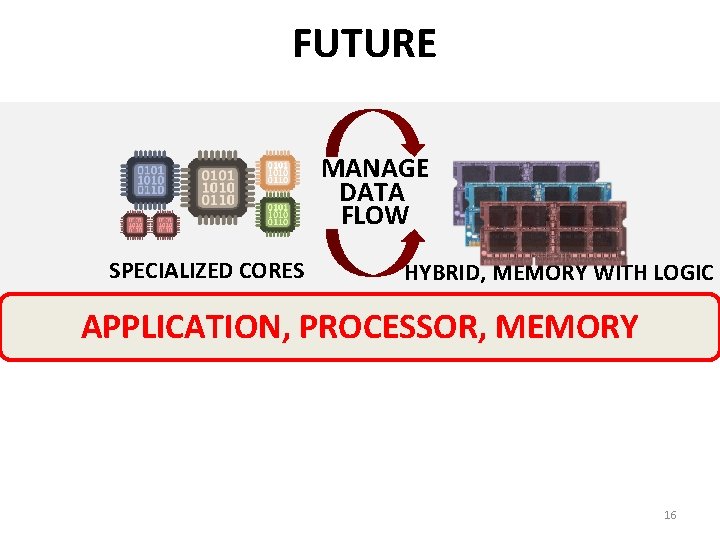
FUTURE MANAGE DATA FLOW SPECIALIZED CORES HYBRID, MEMORY WITH LOGIC APPLICATION, PROCESSOR, MEMORY 16

MAIN MEMORY BASICS

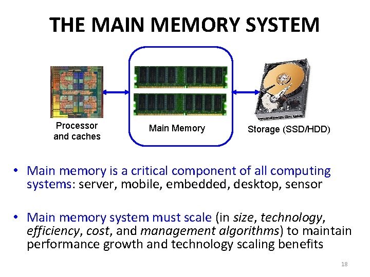
THE MAIN MEMORY SYSTEM Processor and caches Main Memory Storage (SSD/HDD) • Main memory is a critical component of all computing systems: server, mobile, embedded, desktop, sensor • Main memory system must scale (in size, technology, efficiency, cost, and management algorithms) to maintain performance growth and technology scaling benefits 18

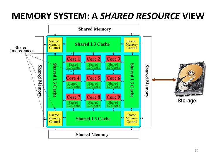
MEMORY SYSTEM: A SHARED RESOURCE VIEW Storage 19

STATE OF THE MAIN MEMORY SYSTEM • Recent technology, architecture, and application trends – lead to new requirements – exacerbate old requirements • DRAM and memory controllers, as we know them today, are (will be) unlikely to satisfy all requirements • Some emerging non-volatile memory technologies (e. g. , PCM) enable new opportunities: memory+storage merging • We need to rethink the main memory system – to fix DRAM issues and enable emerging technologies – to satisfy all requirements 20

MAJOR TRENDS AFFECTING MAIN MEMORY (I) • Need for main memory capacity, bandwidth, Qo. S increasing • Main memory energy/power is a key system design concern • DRAM technology scaling is ending 21

MAJOR TRENDS AFFECTING MAIN MEMORY (II) • Need for main memory capacity, bandwidth, Qo. S increasing – Multi-core: increasing number of cores – Data-intensive applications: increasing demand/hunger for data – Consolidation: cloud computing, GPUs, mobile • Main memory energy/power is a key system design concern • DRAM technology scaling is ending 22

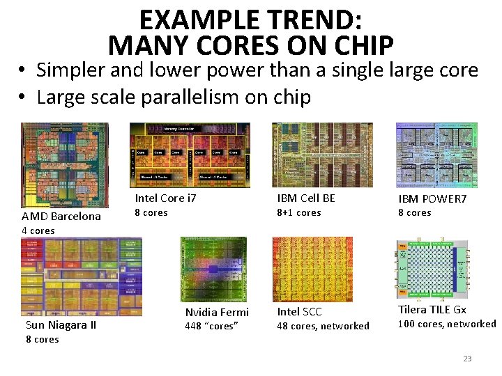
EXAMPLE TREND: MANY CORES ON CHIP • Simpler and lower power than a single large core • Large scale parallelism on chip Intel Core i 7 AMD Barcelona 8 cores IBM Cell BE IBM POWER 7 Intel SCC Tilera TILE Gx 8+1 cores 8 cores 4 cores Sun Niagara II 8 cores Nvidia Fermi 448 “cores” 48 cores, networked 100 cores, networked 23

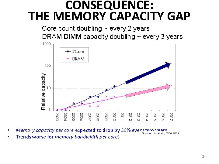
CONSEQUENCE: THE MEMORY CAPACITY GAP Core count doubling ~ every 2 years DRAM DIMM capacity doubling ~ every 3 years • • Memory capacity per core expected to drop by 30% every two years Trends worse for memory bandwidth per core! 24

MAJOR TRENDS AFFECTING MAIN MEMORY (III) • Need for main memory capacity, bandwidth, Qo. S increasing • Main memory energy/power is a key system design concern – ~40 -50% energy spent in off-chip memory hierarchy [Lefurgy, IEEE Computer 2003] – DRAM consumes power even when not used (periodic refresh) • DRAM technology scaling is ending 25

MAJOR TRENDS AFFECTING MAIN MEMORY (IV) • Need for main memory capacity, bandwidth, Qo. S increasing • Main memory energy/power is a key system design concern • DRAM technology scaling is ending – ITRS projects DRAM will not scale easily below X nm – Scaling has provided many benefits: • higher capacity (density), lower cost, lower energy 26

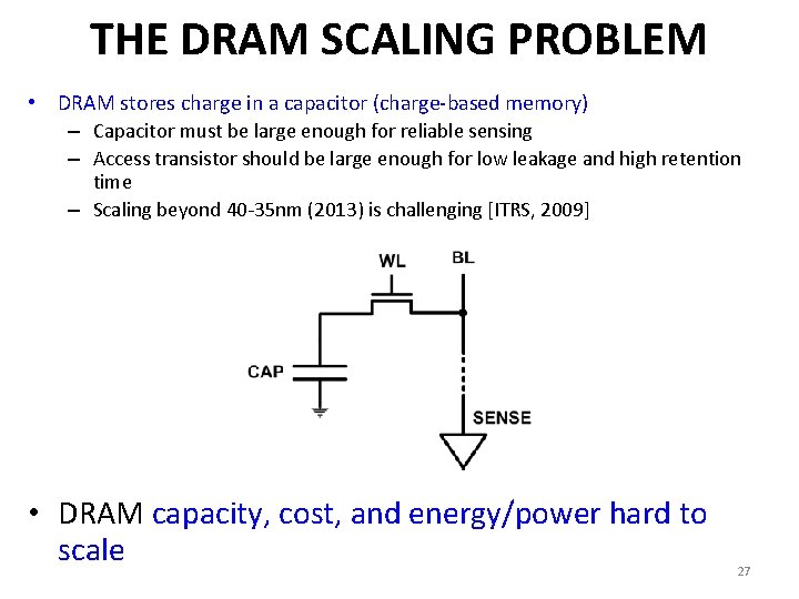
THE DRAM SCALING PROBLEM • DRAM stores charge in a capacitor (charge-based memory) – Capacitor must be large enough for reliable sensing – Access transistor should be large enough for low leakage and high retention time – Scaling beyond 40 -35 nm (2013) is challenging [ITRS, 2009] • DRAM capacity, cost, and energy/power hard to scale 27

SOLUTIONS TO THE DRAM SCALING PROBLEM • Two potential solutions – Tolerate DRAM (by taking a fresh look at it) – Enable emerging memory technologies to eliminate/minimize DRAM • Do both – Hybrid memory systems 28

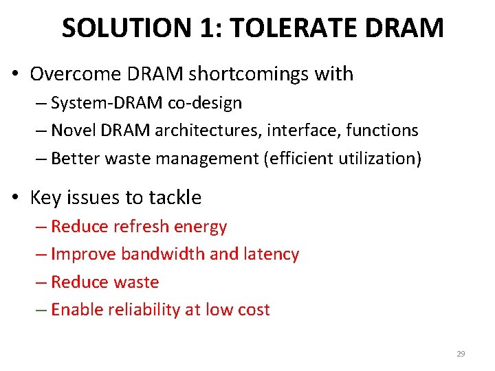
SOLUTION 1: TOLERATE DRAM • Overcome DRAM shortcomings with – System-DRAM co-design – Novel DRAM architectures, interface, functions – Better waste management (efficient utilization) • Key issues to tackle – Reduce refresh energy – Improve bandwidth and latency – Reduce waste – Enable reliability at low cost 29

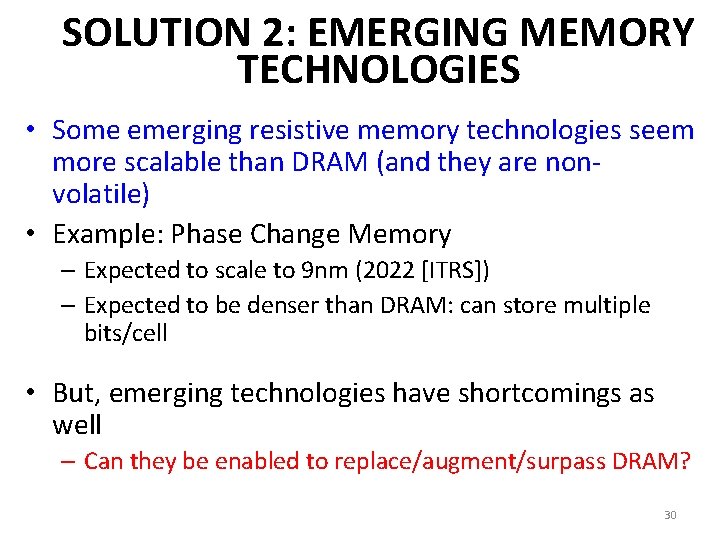
SOLUTION 2: EMERGING MEMORY TECHNOLOGIES • Some emerging resistive memory technologies seem more scalable than DRAM (and they are nonvolatile) • Example: Phase Change Memory – Expected to scale to 9 nm (2022 [ITRS]) – Expected to be denser than DRAM: can store multiple bits/cell • But, emerging technologies have shortcomings as well – Can they be enabled to replace/augment/surpass DRAM? 30

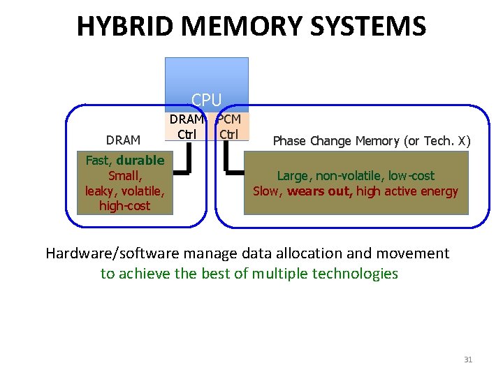
HYBRID MEMORY SYSTEMS CPU DRAM Fast, durable Small, leaky, volatile, high-cost DRAM Ctrl PCM Ctrl Phase Change Memory (or Tech. X) Large, non-volatile, low-cost Slow, wears out, high active energy Hardware/software manage data allocation and movement to achieve the best of multiple technologies 31

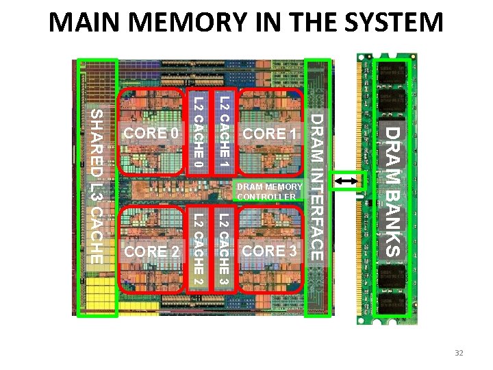
MAIN MEMORY IN THE SYSTEM DRAM BANKS L 2 CACHE 3 L 2 CACHE 2 SHARED L 3 CACHE DRAM MEMORY CONTROLLER DRAM INTERFACE L 2 CACHE 1 L 2 CACHE 0 CORE 3 CORE 2 CORE 1 CORE 0 32

IDEAL MEMORY • • Zero access time (latency) Infinite capacity Zero cost Infinite bandwidth (to support multiple accesses in parallel) 33

THE PROBLEM • Ideal memory’s requirements oppose each other • Bigger is slower – Bigger Takes longer to determine the location • Faster is more expensive – Memory technology: SRAM vs. DRAM • Higher bandwidth is more expensive – Need more banks, more ports, higher frequency, or faster technology 34

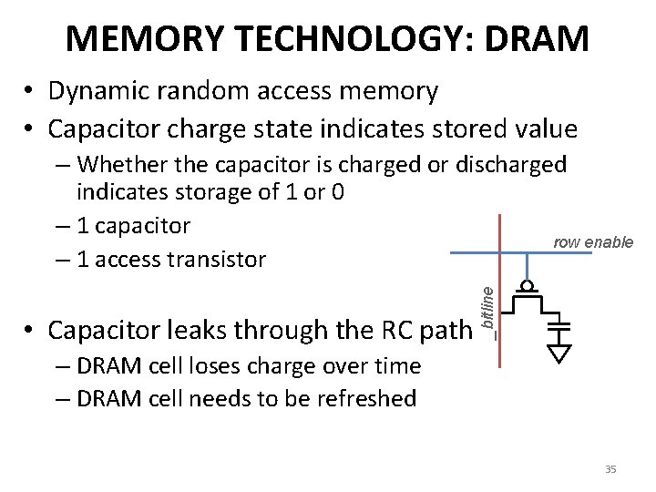
MEMORY TECHNOLOGY: DRAM • Dynamic random access memory • Capacitor charge state indicates stored value • Capacitor leaks through the RC path _bitline – Whether the capacitor is charged or discharged indicates storage of 1 or 0 – 1 capacitor row enable – 1 access transistor – DRAM cell loses charge over time – DRAM cell needs to be refreshed 35

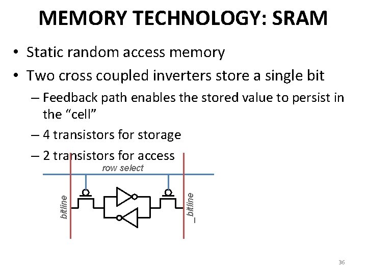
MEMORY TECHNOLOGY: SRAM • Static random access memory • Two cross coupled inverters store a single bit – Feedback path enables the stored value to persist in the “cell” – 4 transistors for storage – 2 transistors for access _bitline row select 36

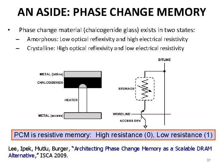
AN ASIDE: PHASE CHANGE MEMORY • Phase change material (chalcogenide glass) exists in two states: – – Amorphous: Low optical reflexivity and high electrical resistivity Crystalline: High optical reflexivity and low electrical resistivity PCM is resistive memory: High resistance (0), Low resistance (1) Lee, Ipek, Mutlu, Burger, “Architecting Phase Change Memory as a Scalable DRAM Alternative, ” ISCA 2009. 37

MEMORY BANK: A FUNDAMENTAL CONCEPT • Interleaving (banking) – Problem: a single monolithic memory array takes long to access and does not enable multiple accesses in parallel – Goal: Reduce the latency of memory array access and enable multiple accesses in parallel – Idea: Divide the array into multiple banks that can be accessed independently (in the same cycle or in consecutive cycles) • Each bank is smaller than the entire memory storage • Accesses to different banks can be overlapped – An issue: How do you map data to different banks? (i. e. , how do you interleave data across banks? ) 38

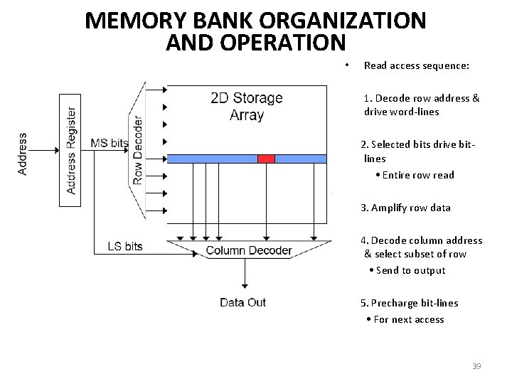
MEMORY BANK ORGANIZATION AND OPERATION • Read access sequence: 1. Decode row address & drive word-lines 2. Selected bits drive bitlines • Entire row read 3. Amplify row data 4. Decode column address & select subset of row • Send to output 5. Precharge bit-lines • For next access 39

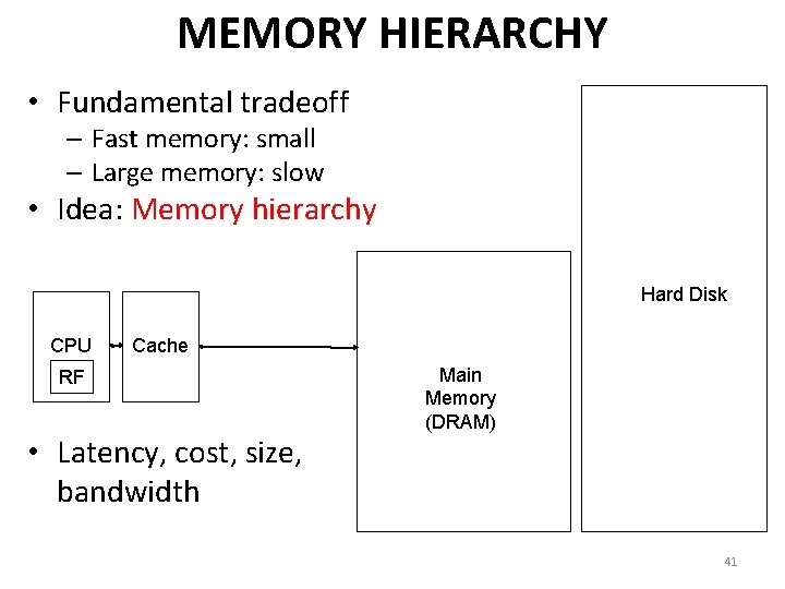
WHY MEMORY HIERARCHY? • We want both fast and large • But we cannot achieve both with a single level of memory • Idea: Have multiple levels of storage (progressively bigger and slower as the levels are farther from the processor) and ensure most of the data the processor needs is kept in the fast(er) level(s) 40

MEMORY HIERARCHY • Fundamental tradeoff – Fast memory: small – Large memory: slow • Idea: Memory hierarchy Hard Disk CPU Cache RF • Latency, cost, size, bandwidth Main Memory (DRAM) 41

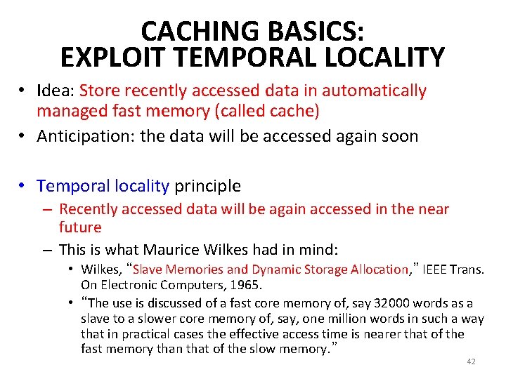
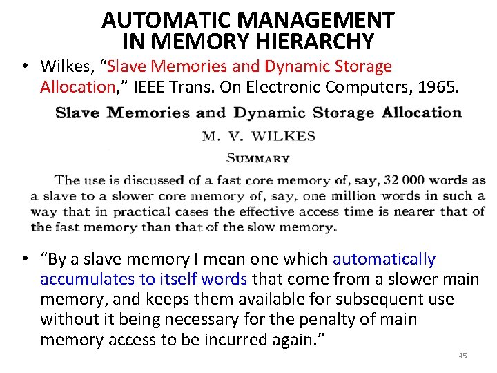
CACHING BASICS: EXPLOIT TEMPORAL LOCALITY • Idea: Store recently accessed data in automatically managed fast memory (called cache) • Anticipation: the data will be accessed again soon • Temporal locality principle – Recently accessed data will be again accessed in the near future – This is what Maurice Wilkes had in mind: • Wilkes, “Slave Memories and Dynamic Storage Allocation, ” IEEE Trans. On Electronic Computers, 1965. • “The use is discussed of a fast core memory of, say 32000 words as a slave to a slower core memory of, say, one million words in such a way that in practical cases the effective access time is nearer that of the fast memory than that of the slow memory. ” 42

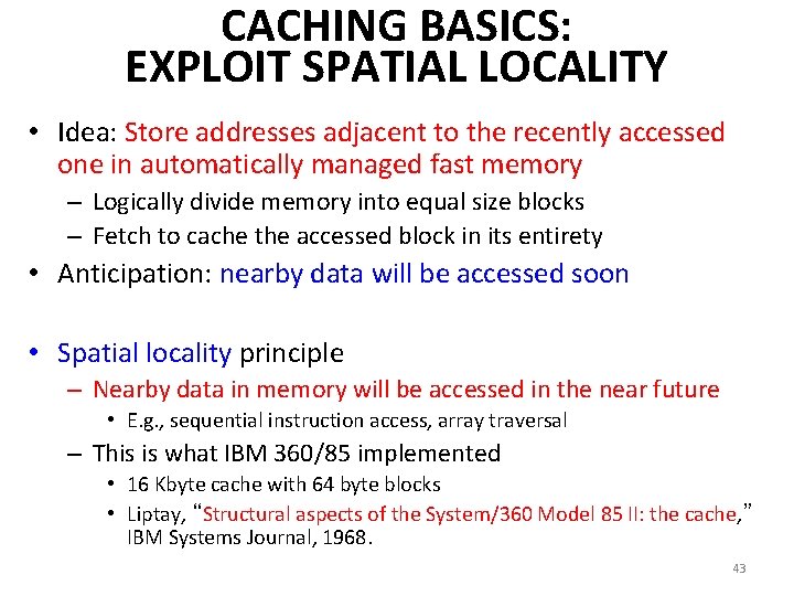
CACHING BASICS: EXPLOIT SPATIAL LOCALITY • Idea: Store addresses adjacent to the recently accessed one in automatically managed fast memory – Logically divide memory into equal size blocks – Fetch to cache the accessed block in its entirety • Anticipation: nearby data will be accessed soon • Spatial locality principle – Nearby data in memory will be accessed in the near future • E. g. , sequential instruction access, array traversal – This is what IBM 360/85 implemented • 16 Kbyte cache with 64 byte blocks • Liptay, “Structural aspects of the System/360 Model 85 II: the cache, ” IBM Systems Journal, 1968. 43

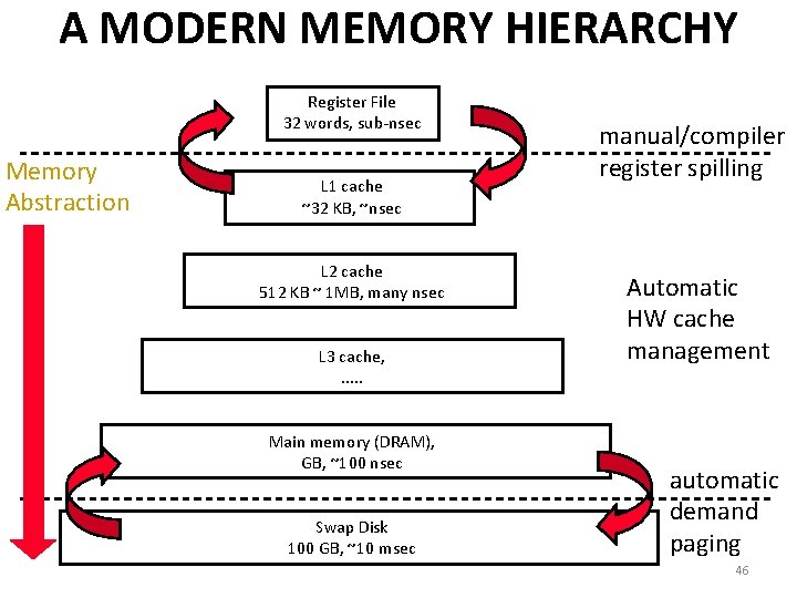
A NOTE ON MANUAL VS. AUTOMATIC MANAGEMENT • Manual: Programmer manages data movement across levels -- too painful for programmers on substantial programs – “core” vs “drum” memory in the 50’s – still done in some embedded processors (on-chip scratch pad SRAM in lieu of a cache) • Automatic: Hardware manages data movement across levels, transparently to the programmer ++ programmer’s life is easier – simple heuristic: keep most recently used items in cache – the average programmer doesn’t need to know about it • You don’t need to know how big the cache is and how it works to write a “correct” program! (What if you want a “fast” program? ) 44

AUTOMATIC MANAGEMENT IN MEMORY HIERARCHY • Wilkes, “Slave Memories and Dynamic Storage Allocation, ” IEEE Trans. On Electronic Computers, 1965. • “By a slave memory I mean one which automatically accumulates to itself words that come from a slower main memory, and keeps them available for subsequent use without it being necessary for the penalty of main memory access to be incurred again. ” 45

A MODERN MEMORY HIERARCHY Register File 32 words, sub-nsec Memory Abstraction L 1 cache ~32 KB, ~nsec L 2 cache 512 KB ~ 1 MB, many nsec L 3 cache, . . . Main memory (DRAM), GB, ~100 nsec Swap Disk 100 GB, ~10 msec manual/compiler register spilling Automatic HW cache management automatic demand paging 46

THE DRAM SUBSYSTEM

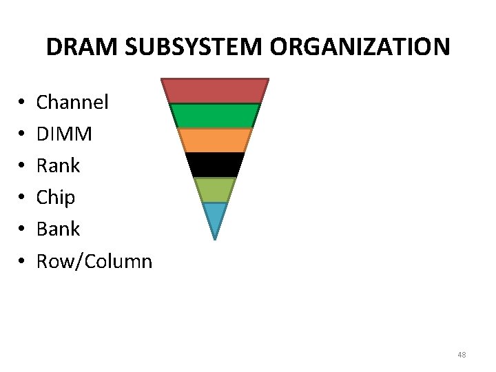
DRAM SUBSYSTEM ORGANIZATION • • • Channel DIMM Rank Chip Bank Row/Column 48

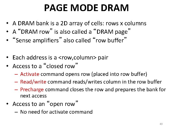
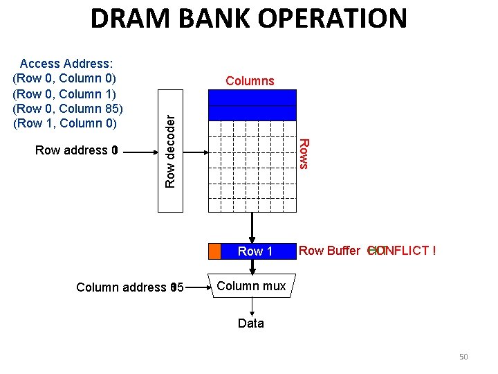
PAGE MODE DRAM • A DRAM bank is a 2 D array of cells: rows x columns • A “DRAM row” is also called a “DRAM page” • “Sense amplifiers” also called “row buffer” • Each address is a <row, column> pair • Access to a “closed row” – Activate command opens row (placed into row buffer) – Read/write command reads/writes column in the row buffer – Precharge command closes the row and prepares the bank for next access • Access to an “open row” – No need for activate command 49

DRAM BANK OPERATION Rows Row address 0 1 Columns Row decoder Access Address: (Row 0, Column 0) (Row 0, Column 1) (Row 0, Column 85) (Row 1, Column 0) Row 01 Row Empty Column address 0 1 85 Row Buffer CONFLICT HIT ! Column mux Data 50

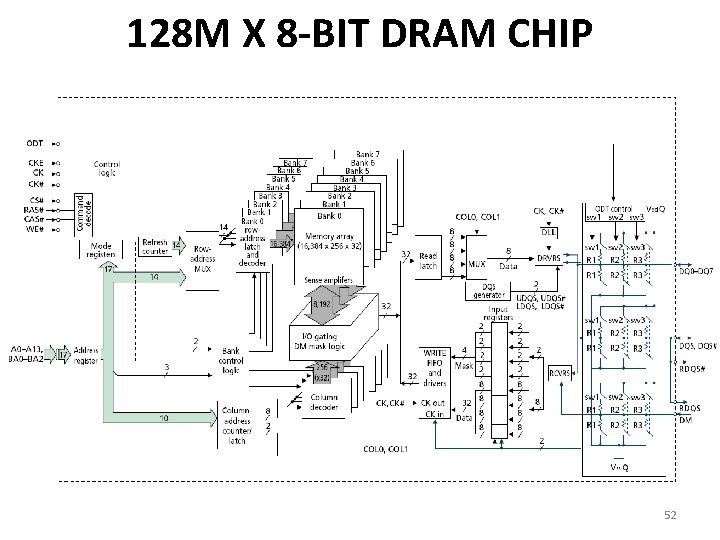
THE DRAM CHIP • Consists of multiple banks (2 -16 in Synchronous DRAM) • Banks share command/address/data buses • The chip itself has a narrow interface (4 -16 bits per read) 51

128 M X 8 -BIT DRAM CHIP 52

COMPUTER ARCHITECTURE CS 6354 Main Memory Samira Khan University of Virginia Mar 3, 2016 The content and concept of this course are adapted from CMU ECE 740