The Microarchitecture of the Pentium 4 processor Glenn

- Slides: 30

The Microarchitecture of the Pentium 4 processor Glenn Hinton, Dave Sager, Mike Upton, Darrell Boggs, Doug Carmean, Alan Kyker, Patrice Roussel. Presented by : Ajay Sharma 6/6/2021 1

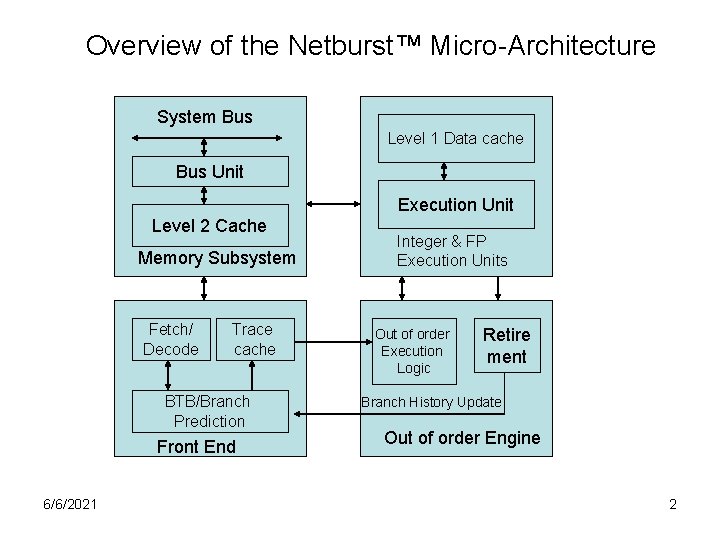
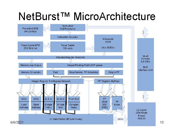
Overview of the Netburst™ Micro-Architecture System Bus Level 1 Data cache Bus Unit Execution Unit Level 2 Cache Memory Subsystem Fetch/ Decode Trace cache BTB/Branch Prediction Front End 6/6/2021 Integer & FP Execution Units Out of order Execution Logic Retire ment Branch History Update Out of order Engine 2

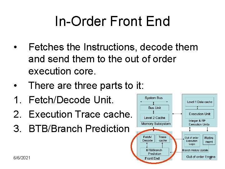
In-Order Front End • Fetches the Instructions, decode them and send them to the out of order execution core. • There are three parts to it: 1. Fetch/Decode Unit. 2. Execution Trace cache. 3. BTB/Branch Prediction 6/6/2021 3

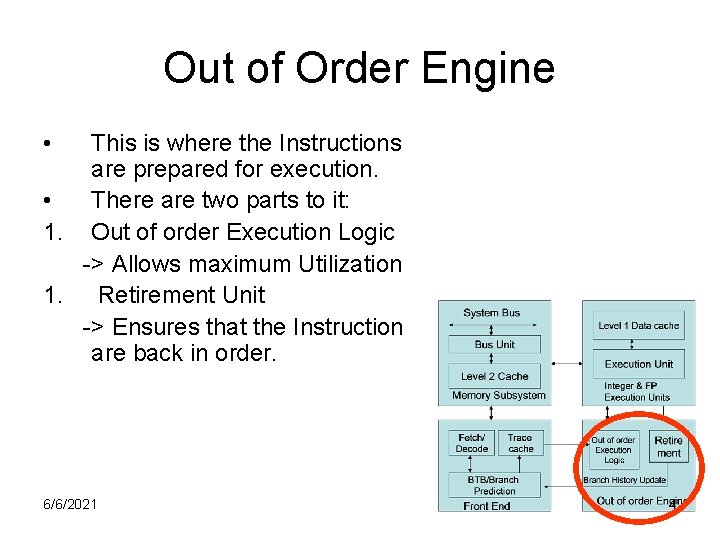
Out of Order Engine • This is where the Instructions are prepared for execution. • There are two parts to it: 1. Out of order Execution Logic -> Allows maximum Utilization 1. Retirement Unit -> Ensures that the Instruction are back in order. 6/6/2021 4

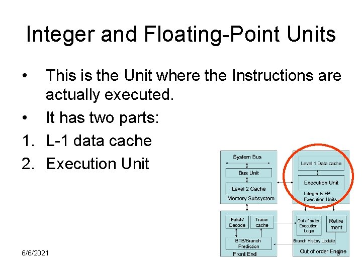
Integer and Floating-Point Units • This is the Unit where the Instructions are actually executed. • It has two parts: 1. L-1 data cache 2. Execution Unit 6/6/2021 5

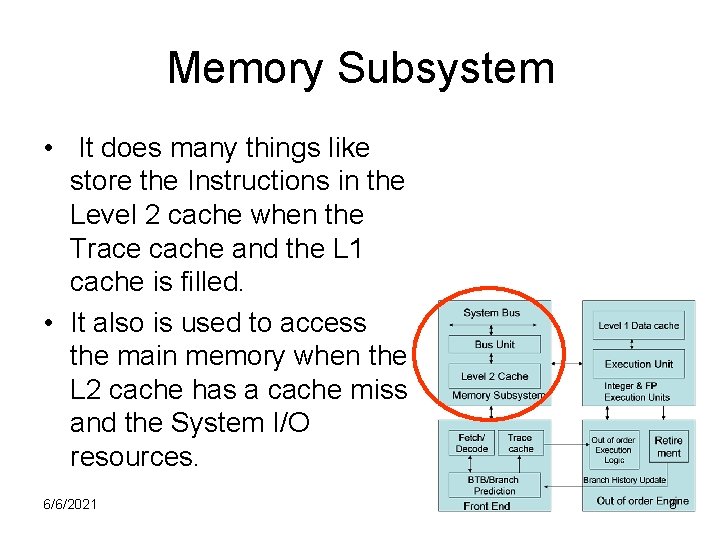
Memory Subsystem • It does many things like store the Instructions in the Level 2 cache when the Trace cache and the L 1 cache is filled. • It also is used to access the main memory when the L 2 cache has a cache miss and the System I/O resources. 6/6/2021 6

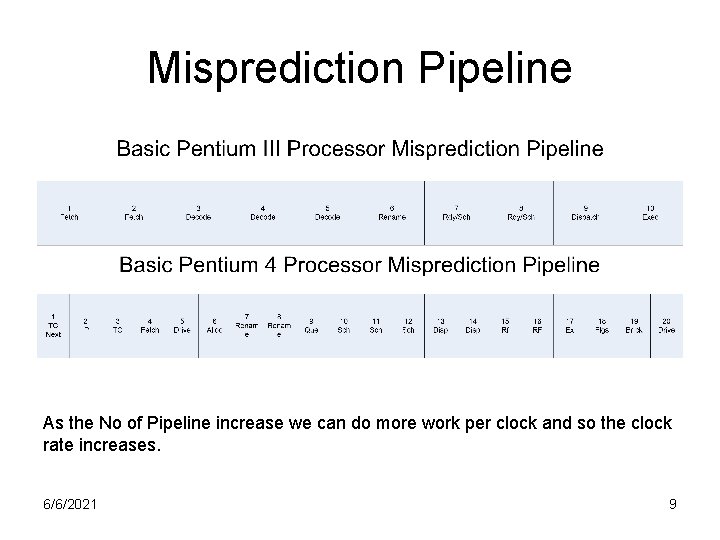
Clock Rates • Clock rates determine the stages of pipeline. • Higher clock rate actually require deeper pipeline and more time for cache miss and mispredicted branch. • But overall they are performance booster. • Say 50% increase in frequency results in only 30% increase in the Net Performance but that is still good. 6/6/2021 7

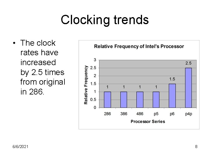
Clocking trends • The clock rates have increased by 2. 5 times from original in 286. 6/6/2021 8

Misprediction Pipeline As the No of Pipeline increase we can do more work per clock and so the clock rate increases. 6/6/2021 9

Net. Burst™ Micro. Architecture 6/6/2021 10

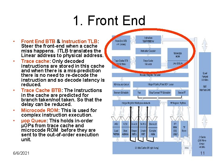
1. Front End • • • Front End BTB & Instruction TLB: Steer the front-end when a cache miss happens. ITLB translates the Linear address to physical address. Trace cache: Only decoded instructions are stored in this cache and when there is a mis-prediction there is no need to re-decode the instruction and so decode latency is reduced. Trace Cache BTB: The Instructions in the cache are predicted for branch taken/not taken. So that the delay can be reduced. Microcode ROM: This is used for complex instruction execution. µop Queue: This holds in-order µOPs from trace cache and microcode ROM before they are sent to the out-of-order execution unit. 6/6/2021 11

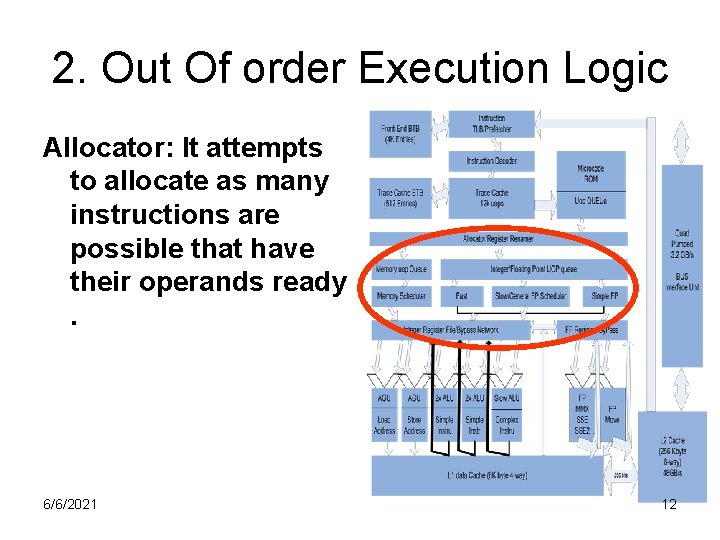
2. Out Of order Execution Logic Allocator: It attempts to allocate as many instructions are possible that have their operands ready. 6/6/2021 12

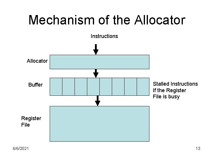
Mechanism of the Allocator Instructions Allocator Buffer Stalled Instructions If the Register File is busy Register File 6/6/2021 13

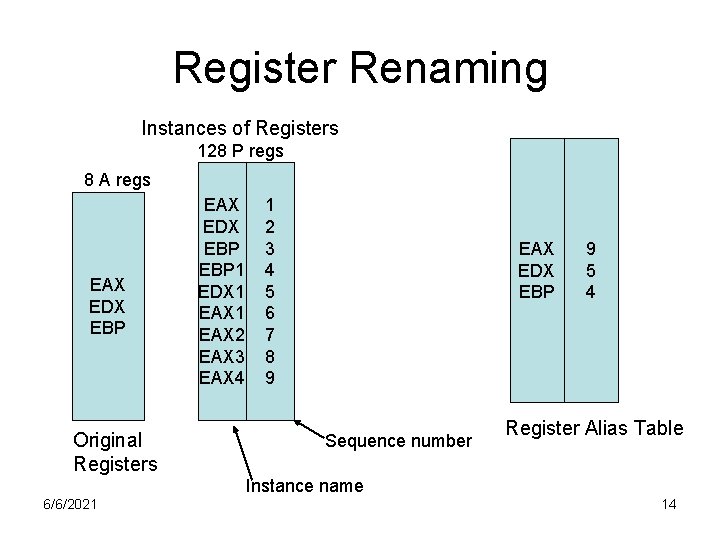
Register Renaming Instances of Registers 128 P regs 8 A regs EAX EDX EBP Original Registers EAX EDX EBP 1 EDX 1 EAX 2 EAX 3 EAX 4 1 2 3 4 5 6 7 8 9 EAX EDX EBP Sequence number 9 5 4 Register Alias Table Instance name 6/6/2021 14

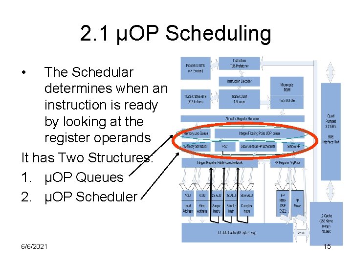
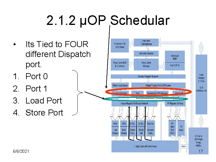
2. 1 µOP Scheduling • The Schedular determines when an instruction is ready by looking at the register operands It has Two Structures: 1. µOP Queues 2. µOP Scheduler 6/6/2021 15

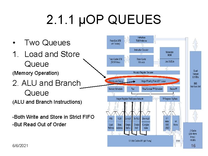
2. 1. 1 µOP QUEUES • Two Queues 1. Load and Store Queue (Memory Operation) 2. ALU and Branch Queue (ALU and Branch Instructions) -Both Write and Store in Strict FIFO -But Read Out of Order 6/6/2021 16

2. 1. 2 µOP Schedular • 1. 2. 3. 4. Its Tied to FOUR different Dispatch port. Port 0 Port 1 Load Port Store Port 6/6/2021 17

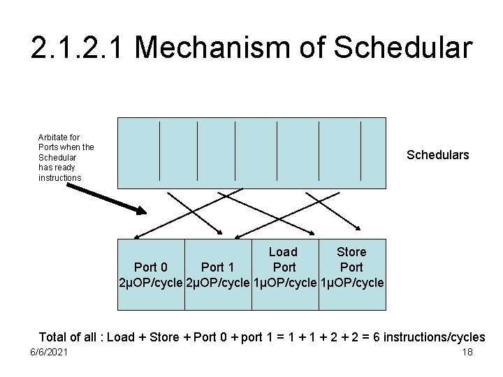
2. 1 Mechanism of Schedular Arbitate for Ports when the Schedular has ready instructions Schedulars Load Store Port 0 Port 1 2µOP/cycle 1µOP/cycle Total of all : Load + Store + Port 0 + port 1 = 1 + 2 + 2 = 6 instructions/cycles 6/6/2021 18

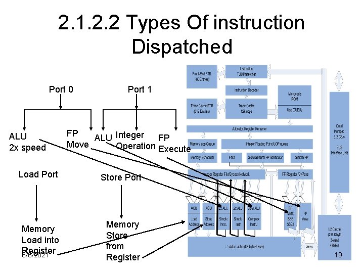
2. 1. 2. 2 Types Of instruction Dispatched Port 0 ALU 2 x speed Port 1 FP ALU Integer FP Move Operation Execute Load Port Store Port Memory Load into Register 6/6/2021 Memory Store from Register 19

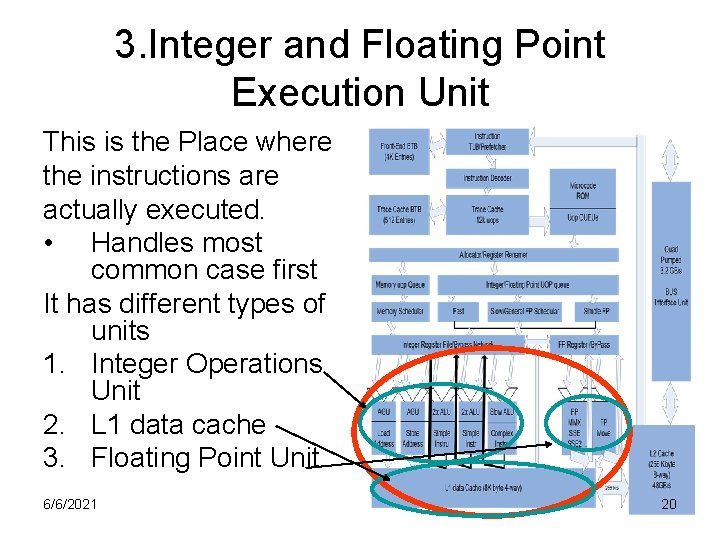
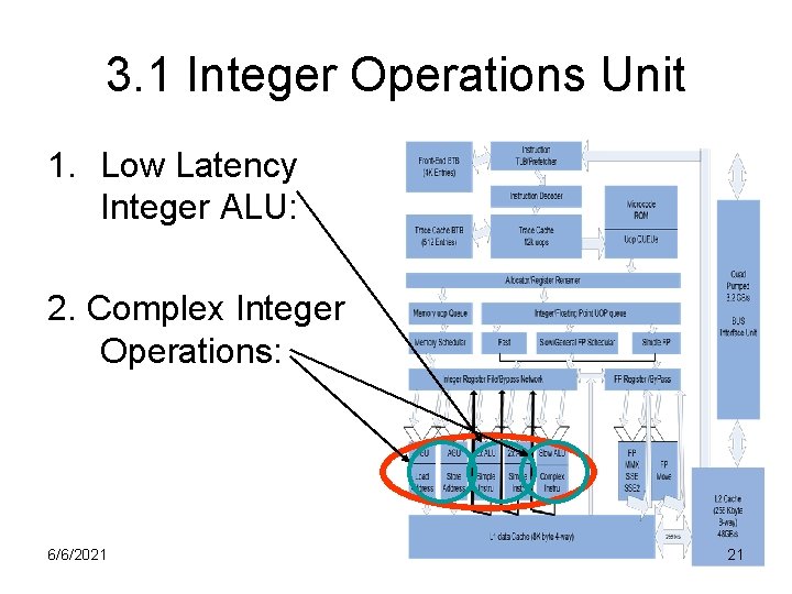
3. Integer and Floating Point Execution Unit This is the Place where the instructions are actually executed. • Handles most common case first It has different types of units 1. Integer Operations Unit 2. L 1 data cache 3. Floating Point Unit 6/6/2021 20

3. 1 Integer Operations Unit 1. Low Latency Integer ALU: 2. Complex Integer Operations: 6/6/2021 21

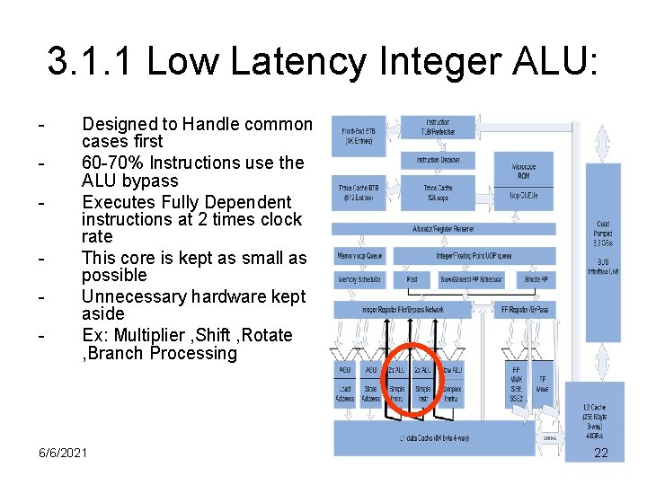
3. 1. 1 Low Latency Integer ALU: - Designed to Handle common cases first 60 -70% Instructions use the ALU bypass Executes Fully Dependent instructions at 2 times clock rate This core is kept as small as possible Unnecessary hardware kept aside Ex: Multiplier , Shift , Rotate , Branch Processing 6/6/2021 22

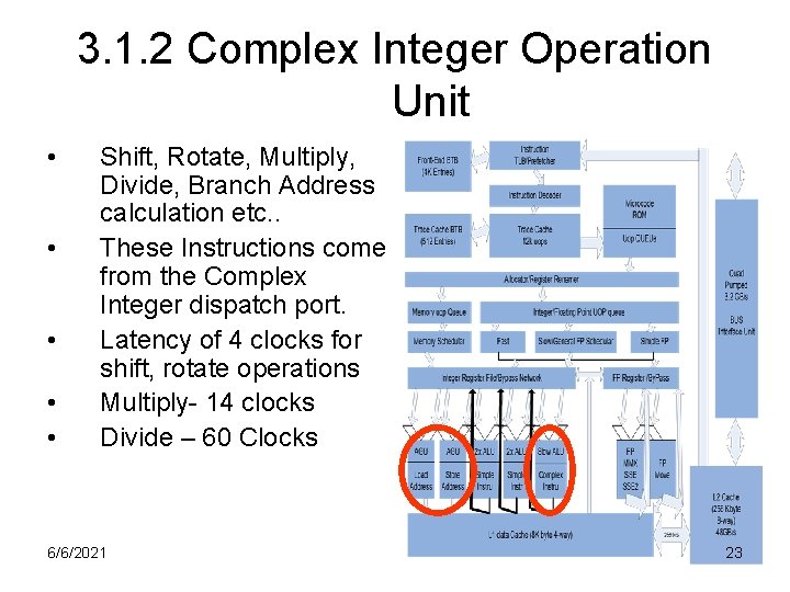
3. 1. 2 Complex Integer Operation Unit • • • Shift, Rotate, Multiply, Divide, Branch Address calculation etc. . These Instructions come from the Complex Integer dispatch port. Latency of 4 clocks for shift, rotate operations Multiply- 14 clocks Divide – 60 Clocks 6/6/2021 23

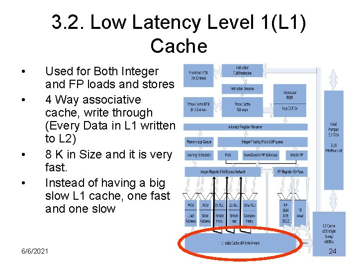
3. 2. Low Latency Level 1(L 1) Cache • • Used for Both Integer and FP loads and stores 4 Way associative cache, write through (Every Data in L 1 written to L 2) 8 K in Size and it is very fast. Instead of having a big slow L 1 cache, one fast and one slow 6/6/2021 24

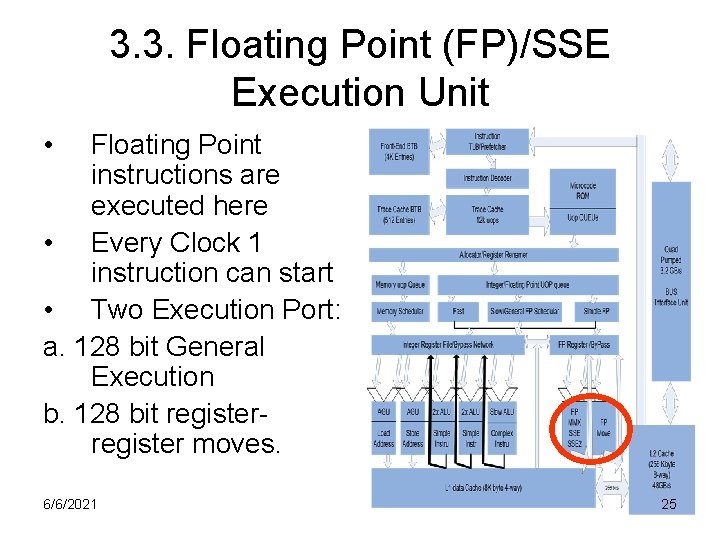
3. 3. Floating Point (FP)/SSE Execution Unit • Floating Point instructions are executed here • Every Clock 1 instruction can start • Two Execution Port: a. 128 bit General Execution b. 128 bit register moves. 6/6/2021 25

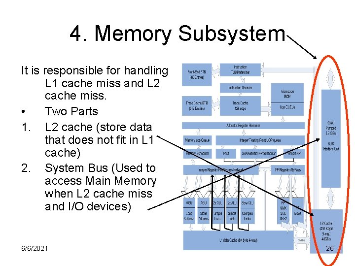
4. Memory Subsystem It is responsible for handling L 1 cache miss and L 2 cache miss. • Two Parts 1. L 2 cache (store data that does not fit in L 1 cache) 2. System Bus (Used to access Main Memory when L 2 cache miss and I/O devices) 6/6/2021 26

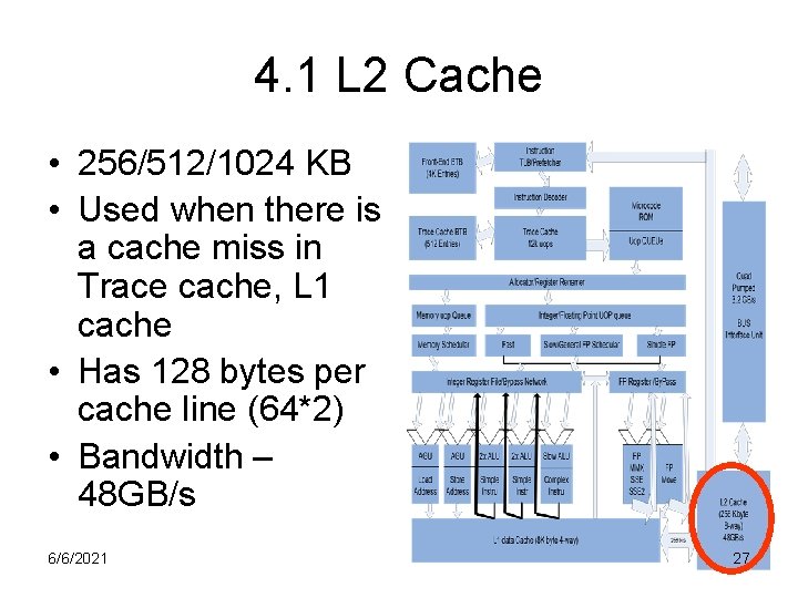
4. 1 L 2 Cache • 256/512/1024 KB • Used when there is a cache miss in Trace cache, L 1 cache • Has 128 bytes per cache line (64*2) • Bandwidth – 48 GB/s 6/6/2021 27

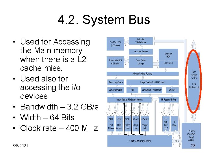
4. 2. System Bus • Used for Accessing the Main memory when there is a L 2 cache miss. • Used also for accessing the i/o devices • Bandwidth – 3. 2 GB/s • Width – 64 Bits • Clock rate – 400 MHz 6/6/2021 28

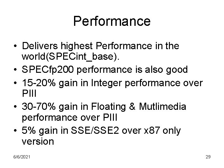
Performance • Delivers highest Performance in the world(SPECint_base). • SPECfp 200 performance is also good • 15 -20% gain in Integer performance over PIII • 30 -70% gain in Floating & Mutlimedia performance over PIII • 5% gain in SSE/SSE 2 over x 87 only version 6/6/2021 29

Thank you Questions? 6/6/2021 30