Computer Architecture CS 3330 Main Memory Samira Khan





- Slides: 51

Computer Architecture CS 3330 Main Memory Samira Khan University of Virginia Apr 14, 2020 The content and concept of this course are adapted from CMU ECE 447

AGENDA • Logistics • Review from last lecture • Memory 2

LOGISTICS • HW 5: Extra Credit – Out Apr 15, 2020 – Due Apr 22, 2020 • Exam 2 – Apr 28, 2020 – Take-home exam – Lecture 12 -23 – Branch prediction important! – Practice homework questions 3

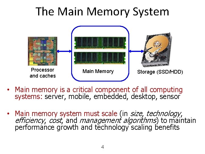
The Main Memory System Processor and caches Main Memory Storage (SSD/HDD) • Main memory is a critical component of all computing systems: server, mobile, embedded, desktop, sensor • Main memory system must scale (in size, technology, efficiency, cost, and management algorithms) to maintain performance growth and technology scaling benefits 4

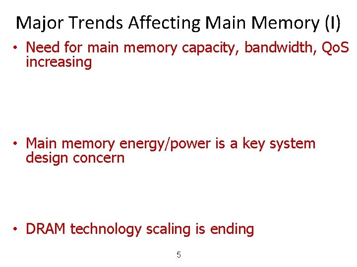
Major Trends Affecting Main Memory (I) • Need for main memory capacity, bandwidth, Qo. S increasing • Main memory energy/power is a key system design concern • DRAM technology scaling is ending 5

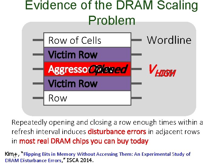
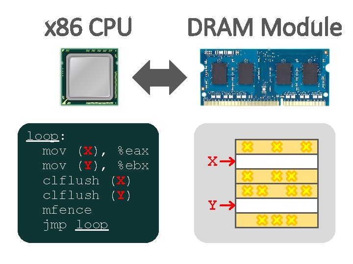
Evidence of the DRAM Scaling Problem Row of Cells Victim Row Aggressor Row Opened Closed Victim Row Row Wordline VHIGH LOW Repeatedly opening and closing a row enough times within a refresh interval induces disturbance errors in adjacent rows in most real DRAM chips you can buy today Kim+, 6 “Flipping Bits in Memory Without Accessing Them: An Experimental Study of DRAM Disturbance Errors, ” ISCA 2014.

x 86 CPU loop: mov (X), %eax mov (Y), %ebx clflush (X) clflush (Y) mfence jmp loop DRAM Module X Y

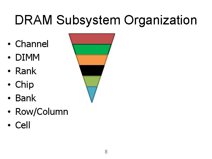
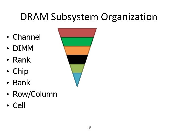
DRAM Subsystem Organization • • Channel DIMM Rank Chip Bank Row/Column Cell 8

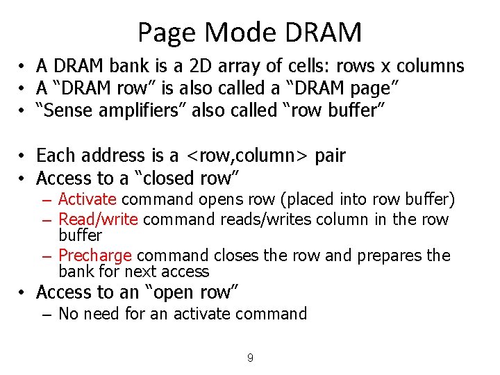
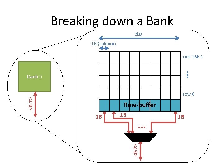
Page Mode DRAM • A DRAM bank is a 2 D array of cells: rows x columns • A “DRAM row” is also called a “DRAM page” • “Sense amplifiers” also called “row buffer” • Each address is a <row, column> pair • Access to a “closed row” – Activate command opens row (placed into row buffer) – Read/write command reads/writes column in the row buffer – Precharge command closes the row and prepares the bank for next access • Access to an “open row” – No need for an activate command 9

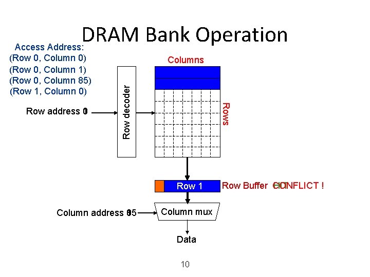
DRAM Bank Operation Access Address: Rows Row address 0 1 Columns Row decoder (Row 0, Column 0) (Row 0, Column 1) (Row 0, Column 85) (Row 1, Column 0) Row 01 Row Empty Column address 0 1 85 Column mux Data 10 Row Buffer CONFLICT HIT !

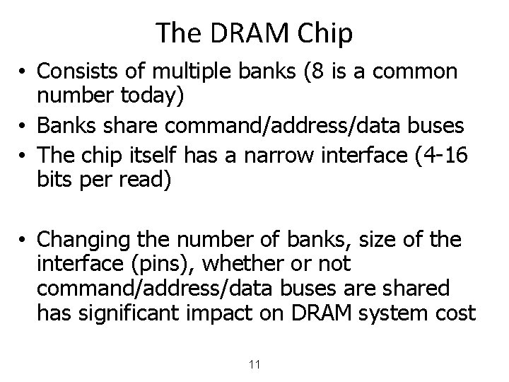
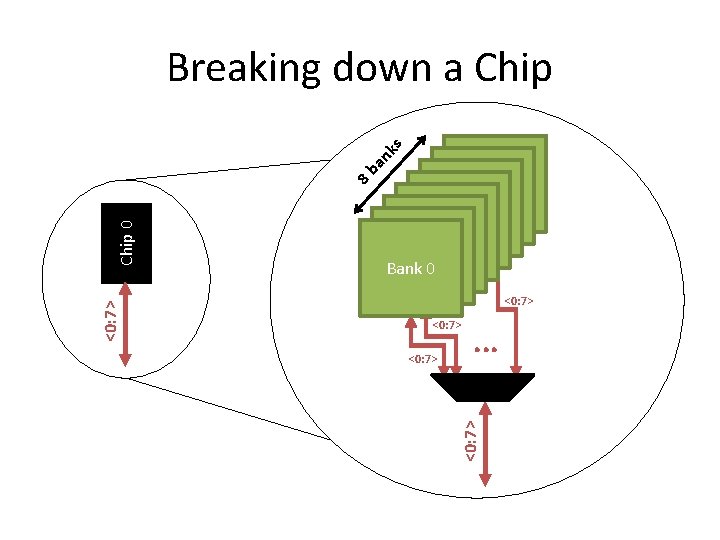
The DRAM Chip • Consists of multiple banks (8 is a common number today) • Banks share command/address/data buses • The chip itself has a narrow interface (4 -16 bits per read) • Changing the number of banks, size of the interface (pins), whether or not command/address/data buses are shared has significant impact on DRAM system cost 11

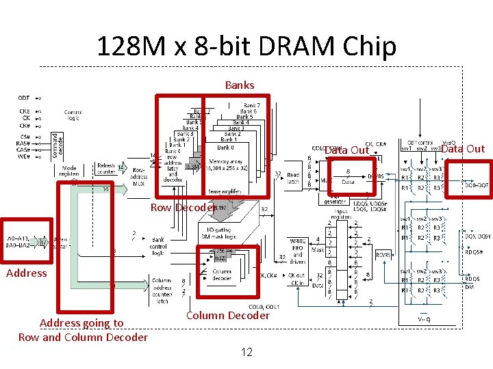
128 M x 8 -bit DRAM Chip Banks Data Out Row Decoder Address going to Row and Column Decoder 12 Data Out

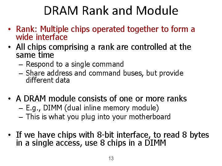
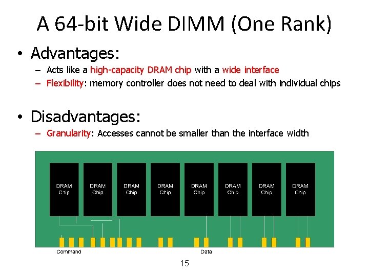
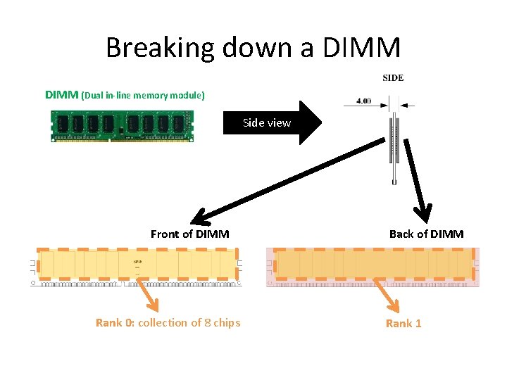
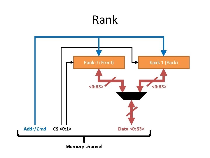
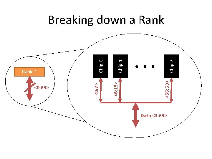
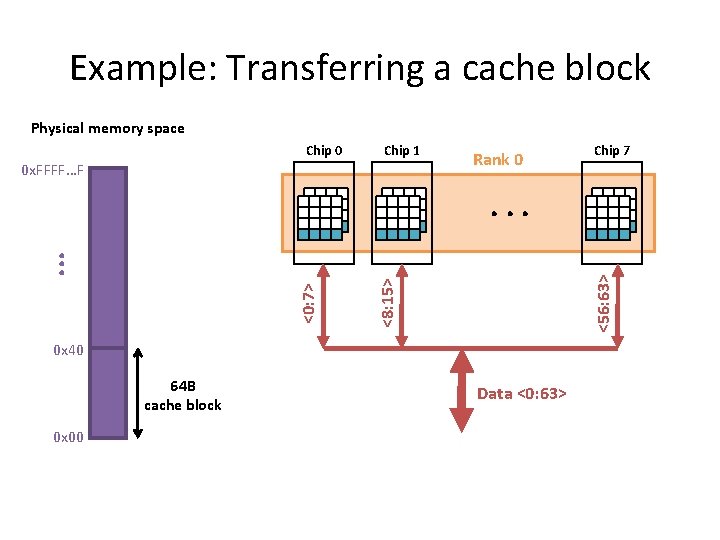
DRAM Rank and Module • Rank: Multiple chips operated together to form a wide interface • All chips comprising a rank are controlled at the same time – Respond to a single command – Share address and command buses, but provide different data • A DRAM module consists of one or more ranks – E. g. , DIMM (dual inline memory module) – This is what you plug into your motherboard • If we have chips with 8 -bit interface, to read 8 bytes in a single access, use 8 chips in a DIMM 13

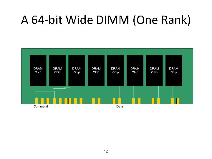
A 64 -bit Wide DIMM (One Rank) 14

A 64 -bit Wide DIMM (One Rank) • Advantages: – Acts like a high-capacity DRAM chip with a wide interface – Flexibility: memory controller does not need to deal with individual chips • Disadvantages: – Granularity: Accesses cannot be smaller than the interface width 15

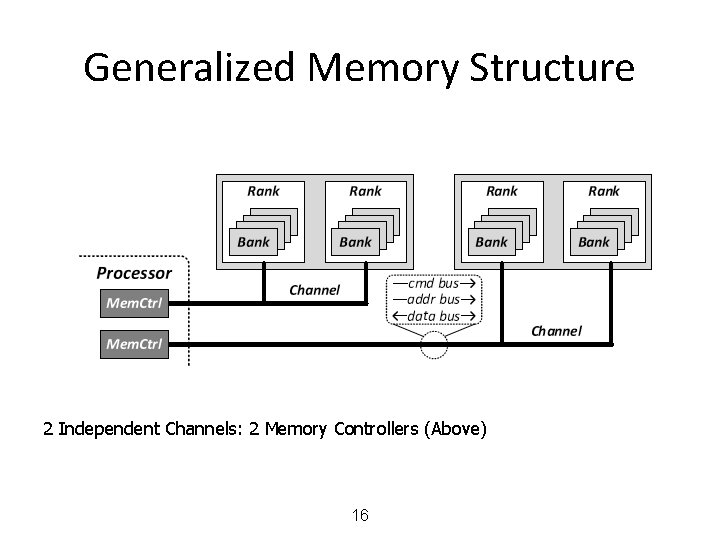
Generalized Memory Structure 2 Independent Channels: 2 Memory Controllers (Above) 16

The DRAM Subsystem The Top Down View

DRAM Subsystem Organization • • Channel DIMM Rank Chip Bank Row/Column Cell 18

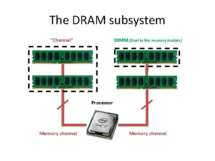
The DRAM subsystem “Channel” DIMM (Dual in-line memory module) Processor Memory channel

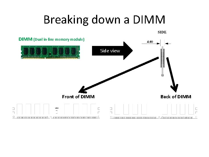
Breaking down a DIMM (Dual in-line memory module) Side view Front of DIMM Back of DIMM

Breaking down a DIMM (Dual in-line memory module) Side view Front of DIMM Rank 0: collection of 8 chips Back of DIMM Rank 1

Rank 0 (Front) Rank 1 (Back) <0: 63> Addr/Cmd CS <0: 1> Memory channel <0: 63> Data <0: 63>

Chip 7 . . . <56: 63> Chip 1 <8: 15> <0: 63> <0: 7> Rank 0 Chip 0 Breaking down a Rank Data <0: 63>

Bank 0 <0: 7> . . . <0: 7> Chip 0 8 b an ks Breaking down a Chip

Breaking down a Bank 2 k. B 1 B (column) row 16 k-1 . . . Bank 0 <0: 7> row 0 Row-buffer 1 B . . . <0: 7> 1 B 1 B

DRAM Subsystem Organization • • Channel DIMM Rank Chip Bank Row/Column Cell 26

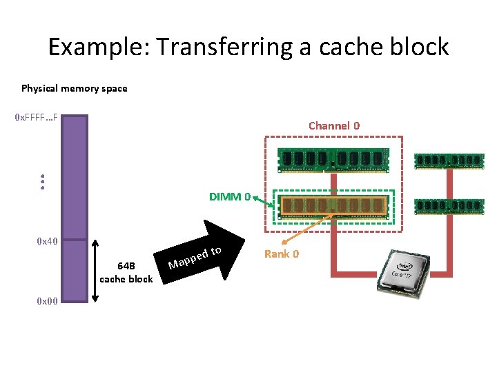
Example: Transferring a cache block Physical memory space 0 x. FFFF…F . . . Channel 0 DIMM 0 0 x 40 64 B cache block 0 x 00 to d e p Map Rank 0

Example: Transferring a cache block Physical memory space Chip 0 Chip 1 0 x. FFFF…F Rank 0 Chip 7 <56: 63> <8: 15> <0: 7> . . . 0 x 40 64 B cache block 0 x 00 Data <0: 63>

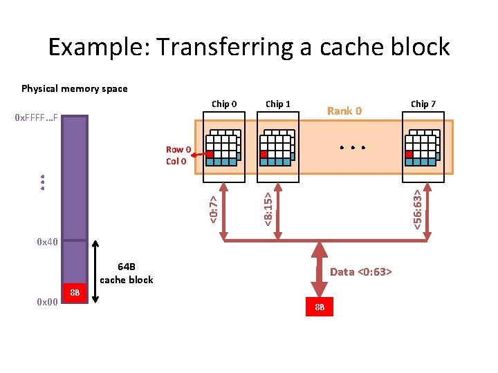
Example: Transferring a cache block Physical memory space Chip 0 Chip 1 0 x. FFFF…F Rank 0 . . . <56: 63> <8: 15> <0: 7> . . . Row 0 Col 0 0 x 40 64 B cache block 0 x 00 Chip 7 Data <0: 63>

Example: Transferring a cache block Physical memory space Chip 0 Chip 1 Rank 0 0 x. FFFF…F . . . <56: 63> <8: 15> <0: 7> . . . Row 0 Col 0 0 x 40 64 B cache block 0 x 00 Chip 7 Data <0: 63> 8 B 8 B

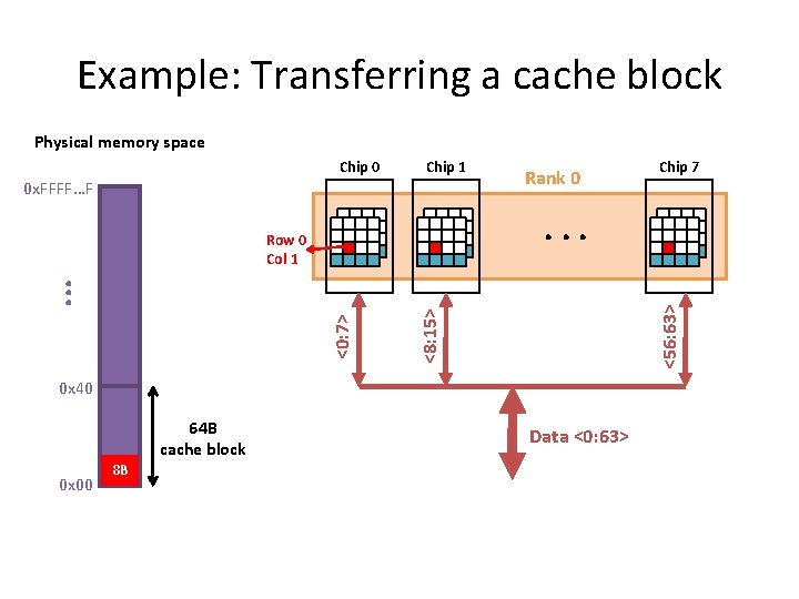
Example: Transferring a cache block Physical memory space Chip 0 Chip 1 0 x. FFFF…F Rank 0 . . . <56: 63> <8: 15> <0: 7> . . . Row 0 Col 1 0 x 40 64 B cache block 0 x 00 8 B Chip 7 Data <0: 63>

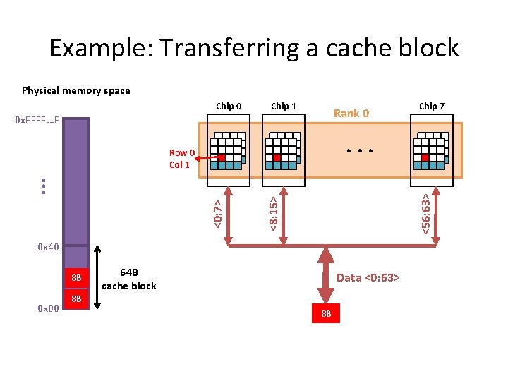
Example: Transferring a cache block Physical memory space Chip 0 Chip 1 Rank 0 0 x. FFFF…F . . . <56: 63> <8: 15> <0: 7> . . . Row 0 Col 1 0 x 40 8 B 0 x 00 Chip 7 64 B cache block Data <0: 63> 8 B 8 B

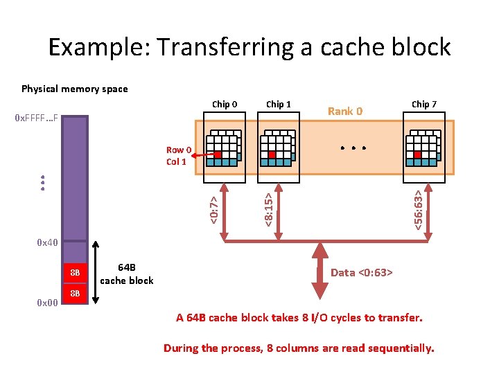
Example: Transferring a cache block Physical memory space Chip 0 Chip 1 0 x. FFFF…F Rank 0 Chip 7 . . . <56: 63> <8: 15> <0: 7> . . . Row 0 Col 1 0 x 40 8 B 0 x 00 64 B cache block Data <0: 63> 8 B A 64 B cache block takes 8 I/O cycles to transfer. During the process, 8 columns are read sequentially.

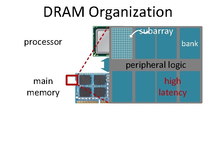
DRAM Organization processor subarray bank peripheral logic main memory high latency

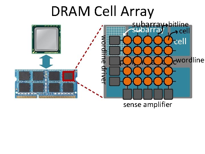
DRAM Cell Array wordline driver subarray bitline subarray cell peripheral logicwordline sense amplifier

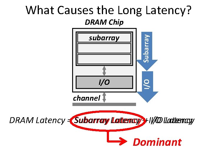
What Causes the Long Latency? I/O subarray cell array Subarray DRAM Chip channel DRAM Latency = Subarray Latency ++ I/O Latency Dominant

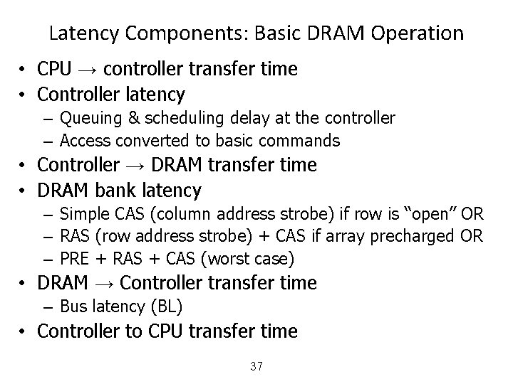
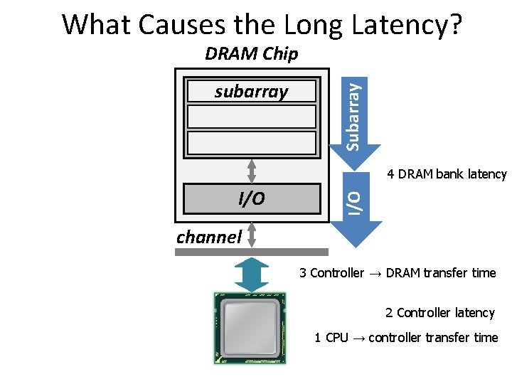
Latency Components: Basic DRAM Operation • CPU → controller transfer time • Controller latency – Queuing & scheduling delay at the controller – Access converted to basic commands • Controller → DRAM transfer time • DRAM bank latency – Simple CAS (column address strobe) if row is “open” OR – RAS (row address strobe) + CAS if array precharged OR – PRE + RAS + CAS (worst case) • DRAM → Controller transfer time – Bus latency (BL) • Controller to CPU transfer time 37

What Causes the Long Latency? subarray cell array Subarray DRAM Chip I/O 4 DRAM bank latency channel 3 Controller → DRAM transfer time 2 Controller latency 1 CPU → controller transfer time

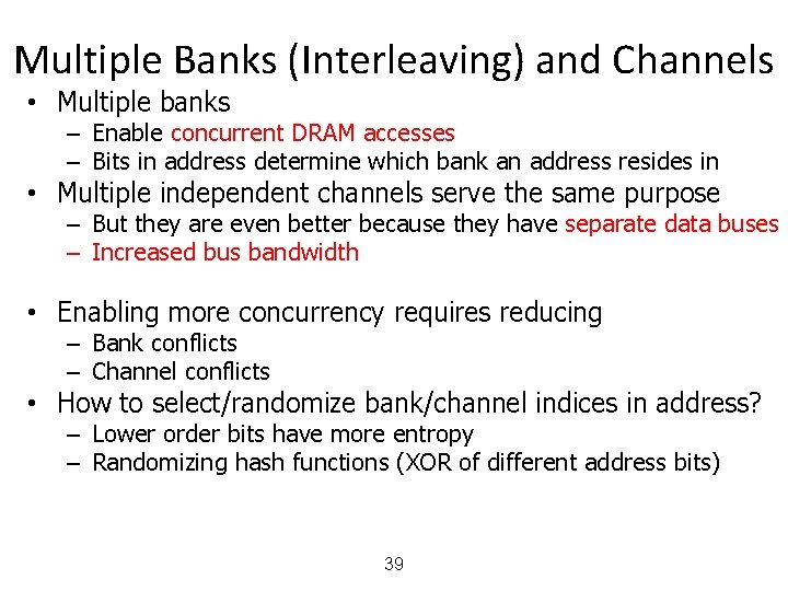
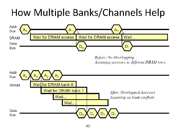
Multiple Banks (Interleaving) and Channels • Multiple banks – Enable concurrent DRAM accesses – Bits in address determine which bank an address resides in • Multiple independent channels serve the same purpose – But they are even better because they have separate data buses – Increased bus bandwidth • Enabling more concurrency requires reducing – Bank conflicts – Channel conflicts • How to select/randomize bank/channel indices in address? – Lower order bits have more entropy – Randomizing hash functions (XOR of different address bits) 39

How Multiple Banks/Channels Help 40

Multiple Channels • Advantages – Increased bandwidth – Multiple concurrent accesses (if independent channels) • Disadvantages – Higher cost than a single channel • More board wires • More pins (if on-chip memory controller) 41

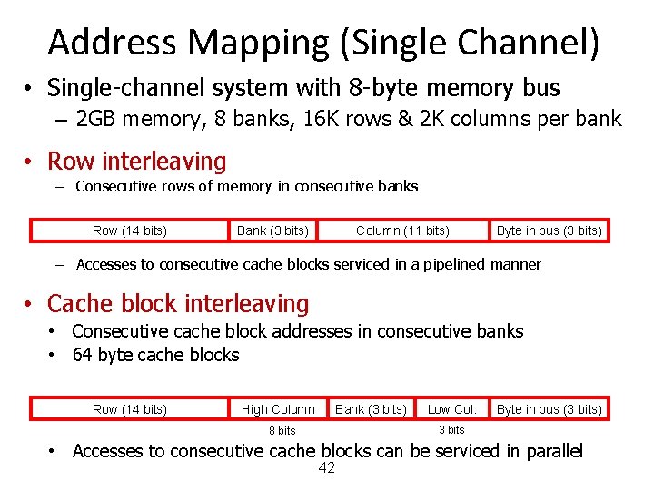
Address Mapping (Single Channel) • Single-channel system with 8 -byte memory bus – 2 GB memory, 8 banks, 16 K rows & 2 K columns per bank • Row interleaving – Consecutive rows of memory in consecutive banks Row (14 bits) Bank (3 bits) Column (11 bits) Byte in bus (3 bits) – Accesses to consecutive cache blocks serviced in a pipelined manner • Cache block interleaving • Consecutive cache block addresses in consecutive banks • 64 byte cache blocks Row (14 bits) High Column Bank (3 bits) Low Col. Byte in bus (3 bits) 3 bits 8 bits • Accesses to consecutive cache blocks can be serviced in parallel 42

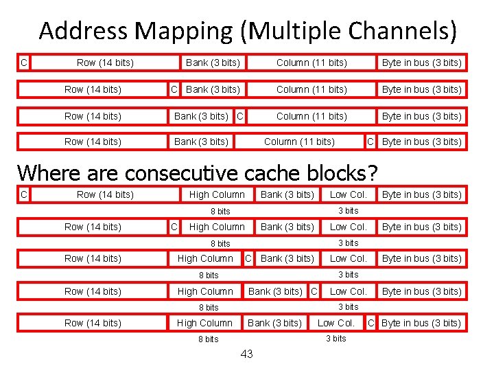
Address Mapping (Multiple Channels) C Row (14 bits) Bank (3 bits) Column (11 bits) Byte in bus (3 bits) Row (14 bits) Bank (3 bits) Column (11 bits) C Byte in bus (3 bits) Where are consecutive cache blocks? C Row (14 bits) High Column Bank (3 bits) Low Col. 3 bits 8 bits Row (14 bits) C High Column Bank (3 bits) Low Col. High Column C Bank (3 bits) Low Col. High Column Bank (3 bits) C High Column Low Col. Byte in bus (3 bits) 3 bits 8 bits Row (14 bits) Byte in bus (3 bits) Bank (3 bits) Low Col. 3 bits 8 bits 43 C Byte in bus (3 bits)

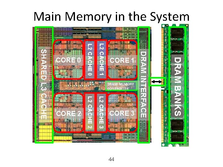
Main Memory in the System 44 DRAM BANKS L 2 CACHE 3 L 2 CACHE 2 SHARED L 3 CACHE DRAM MEMORY CONTROLLER DRAM INTERFACE L 2 CACHE 1 L 2 CACHE 0 CORE 3 CORE 2 CORE 1 CORE 0

MEMORY CONTROLLERS

DRAM VERSUS OTHER TYPES OF MEMORIES • Long latency memories have similar characteristics that need to be controlled. • The following discussion will use DRAM as an example, but many issues are similar in the design of controllers for other types of memories – Flash memory – Other emerging memory technologies • Phase Change Memory • Spin-Transfer Torque Magnetic Memory 46

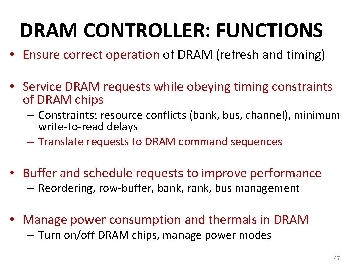
DRAM CONTROLLER: FUNCTIONS • Ensure correct operation of DRAM (refresh and timing) • Service DRAM requests while obeying timing constraints of DRAM chips – Constraints: resource conflicts (bank, bus, channel), minimum write-to-read delays – Translate requests to DRAM command sequences • Buffer and schedule requests to improve performance – Reordering, row-buffer, bank, rank, bus management • Manage power consumption and thermals in DRAM – Turn on/off DRAM chips, manage power modes 47

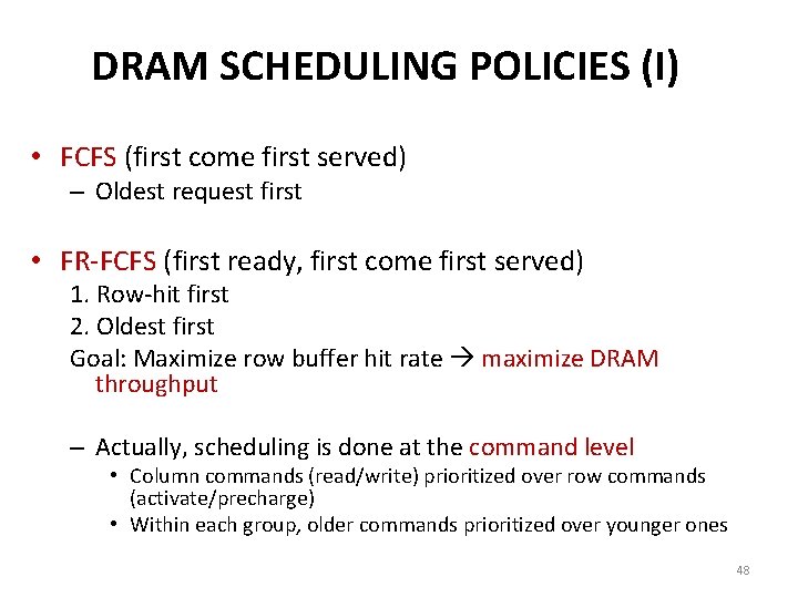
DRAM SCHEDULING POLICIES (I) • FCFS (first come first served) – Oldest request first • FR-FCFS (first ready, first come first served) 1. Row-hit first 2. Oldest first Goal: Maximize row buffer hit rate maximize DRAM throughput – Actually, scheduling is done at the command level • Column commands (read/write) prioritized over row commands (activate/precharge) • Within each group, older commands prioritized over younger ones 48

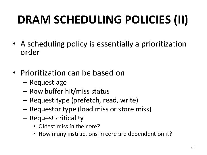
DRAM SCHEDULING POLICIES (II) • A scheduling policy is essentially a prioritization order • Prioritization can be based on – Request age – Row buffer hit/miss status – Request type (prefetch, read, write) – Requestor type (load miss or store miss) – Request criticality • Oldest miss in the core? • How many instructions in core are dependent on it? 49

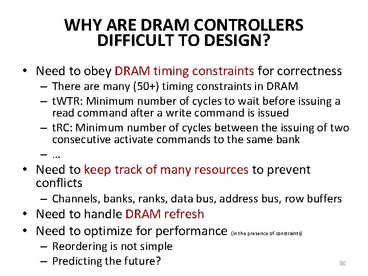
WHY ARE DRAM CONTROLLERS DIFFICULT TO DESIGN? • Need to obey DRAM timing constraints for correctness – There are many (50+) timing constraints in DRAM – t. WTR: Minimum number of cycles to wait before issuing a read command after a write command is issued – t. RC: Minimum number of cycles between the issuing of two consecutive activate commands to the same bank –… • Need to keep track of many resources to prevent conflicts – Channels, banks, ranks, data bus, address bus, row buffers • Need to handle DRAM refresh • Need to optimize for performance – Reordering is not simple – Predicting the future? (in the presence of constraints) 50

Computer Architecture CS 3330 Main Memory Samira Khan University of Virginia Apr 14, 2020 The content and concept of this course are adapted from CMU ECE 447