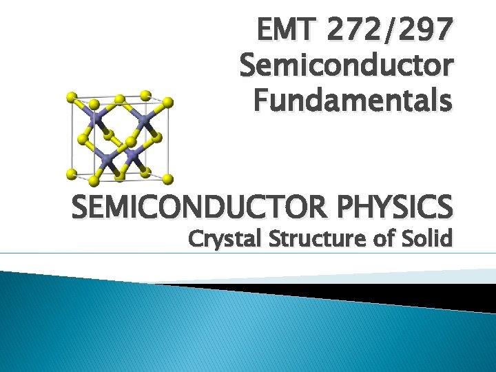
EMT 272297 Semiconductor Fundamentals SEMICONDUCTOR PHYSICS Crystal Structure
- Slides: 40

EMT 272/297 Semiconductor Fundamentals SEMICONDUCTOR PHYSICS Crystal Structure of Solid

Outlines: 1. 2. 3. 4. 5. 6. 7. Solid state materials Semiconductor materials Type of Solids Basic crystal structure Diamond Structure Atomic bonds Crystal growth technique

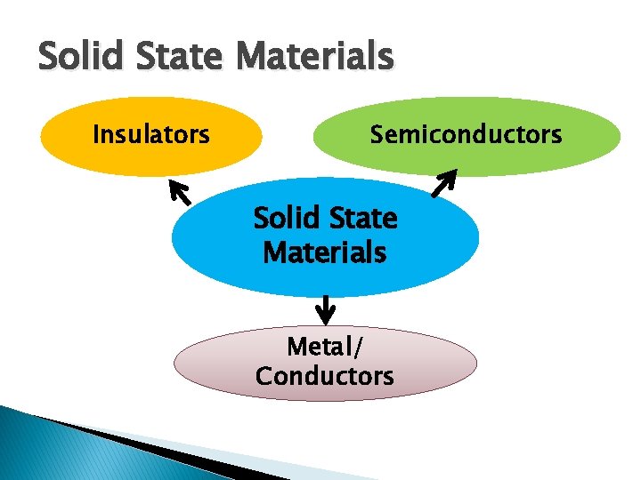
Solid State Materials Insulators Semiconductors Solid State Materials Metal/ Conductors

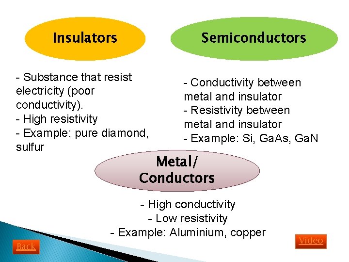
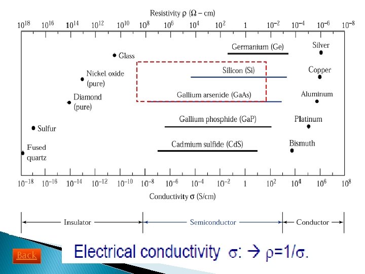
Insulators Semiconductors - Substance that resist electricity (poor conductivity). - High resistivity - Example: pure diamond, sulfur - Conductivity between metal and insulator - Resistivity between metal and insulator - Example: Si, Ga. As, Ga. N Metal/ Conductors - High conductivity - Low resistivity - Example: Aluminium, copper Back Video

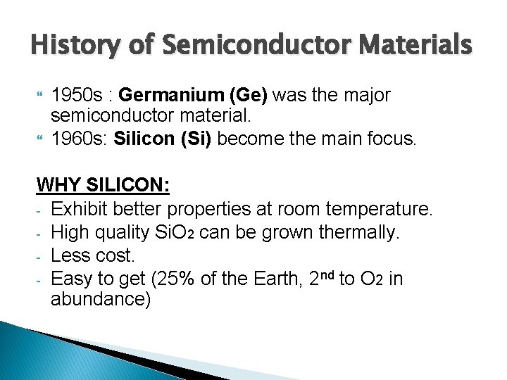
History of Semiconductor Materials 1950 s : Germanium (Ge) was the major semiconductor material. 1960 s: Silicon (Si) become the main focus. WHY SILICON: - Exhibit better properties at room temperature. - High quality Si. O 2 can be grown thermally. - Less cost. - Easy to get (25% of the Earth, 2 nd to O 2 in abundance)

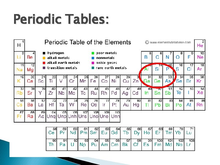
Periodic Tables:

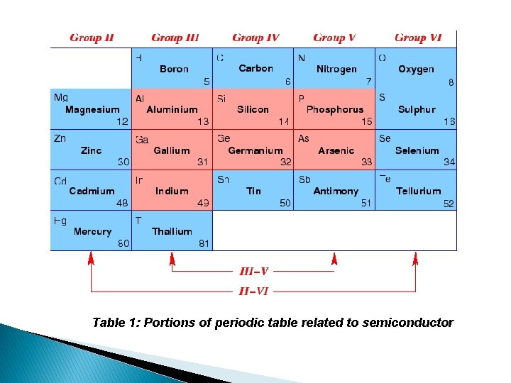
Table 1: Portions of periodic table related to semiconductor

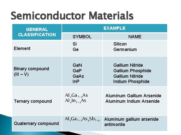
Semiconductor Materials GENERAL CLASSIFICATION EXAMPLE SYMBOL NAME Element Si Ge Silicon Germanium Binary compound (III – V) Ga. N Ga. P Ga. As In. P Gallium Nitride Gallium Phosphide Gallium Nitride Indium Phosphide Ternary compound Quaternary compound Alx. Ga 1 -x. As Alx. In 1 -x. As Aluminum Gallium Arsenide Aluminum Indium Arsenide Alx. Ga 1 -x. Asy. Sb 1 -y Aluminum gallium arsenide antimonite

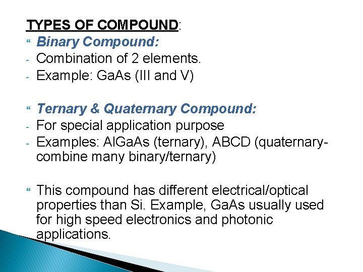
TYPES OF COMPOUND: Binary Compound: - Combination of 2 elements. - Example: Ga. As (III and V) - Ternary & Quaternary Compound: For special application purpose Examples: Al. Ga. As (ternary), ABCD (quaternarycombine many binary/ternary) This compound has different electrical/optical properties than Si. Example, Ga. As usually used for high speed electronics and photonic applications.

Back

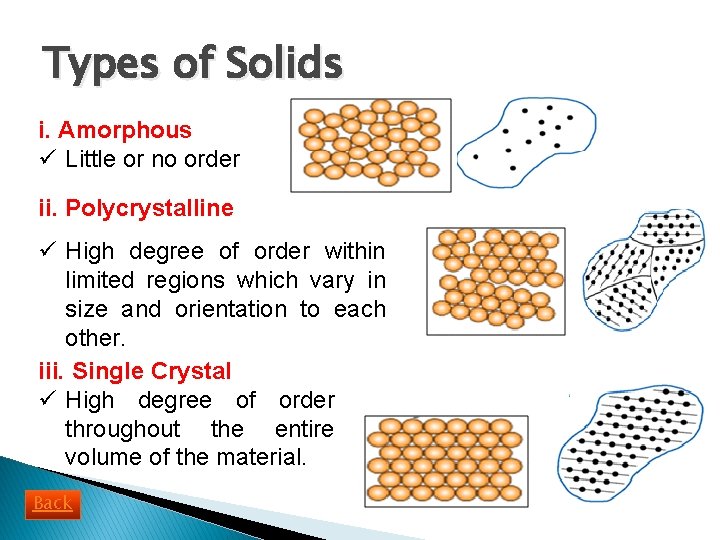
Types of Solids i. Amorphous ü Little or no order ii. Polycrystalline ü High degree of order within limited regions which vary in size and orientation to each other. iii. Single Crystal ü High degree of order throughout the entire volume of the material. Back

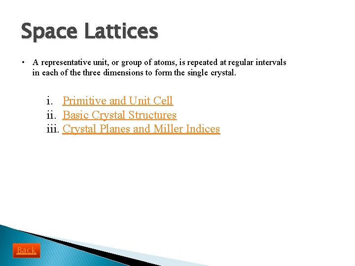
Space Lattices • A representative unit, or group of atoms, is repeated at regular intervals in each of the three dimensions to form the single crystal. i. Primitive and Unit Cell ii. Basic Crystal Structures iii. Crystal Planes and Miller Indices Back

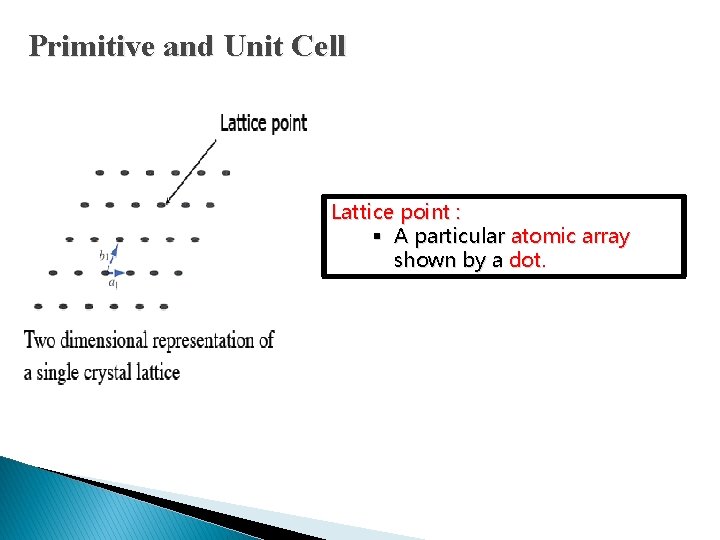
Primitive and Unit Cell Lattice point : § A particular atomic array shown by a dot.

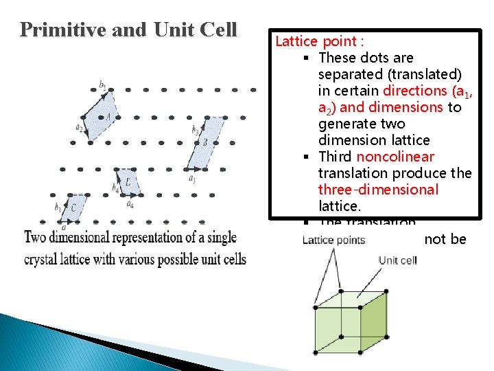
Primitive and Unit Cell Lattice point : § These dots are separated (translated) in certain directions (a 1, a 2) and dimensions to generate two dimension lattice § Third noncolinear translation produce three-dimensional lattice. § The translation directions need not be perpendicular.

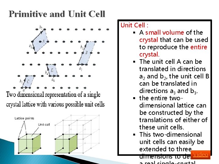
Primitive and Unit Cell : § A small volume of the crystal that can be used to reproduce the entire crystal. § The unit cell A can be translated in directions a 2 and b 2, the unit cell B can be translated in directions a 3 and b 3. § the entire twodimensional lattice can be constructed by the translations of either of these unit cells. § This two-dimensional unit cells can easily be extended to three Video dimensions to describe

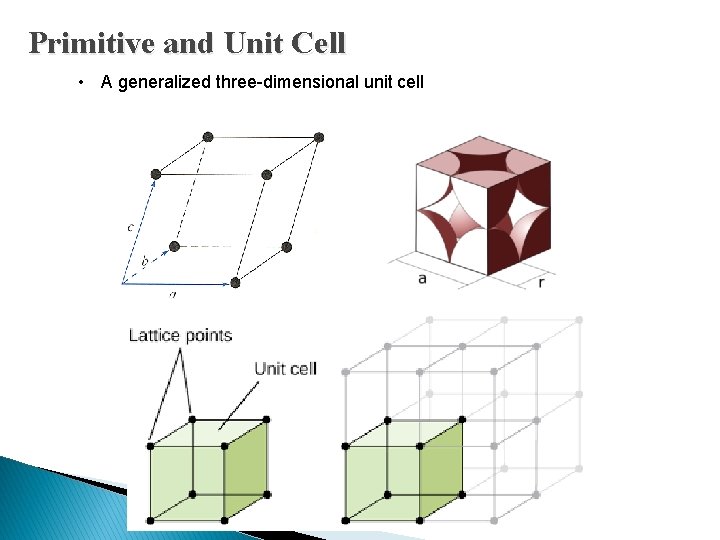
Primitive and Unit Cell • A generalized three-dimensional unit cell

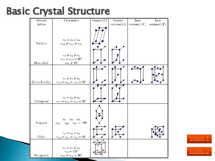
Basic Crystal Structure Video 1 Video 2

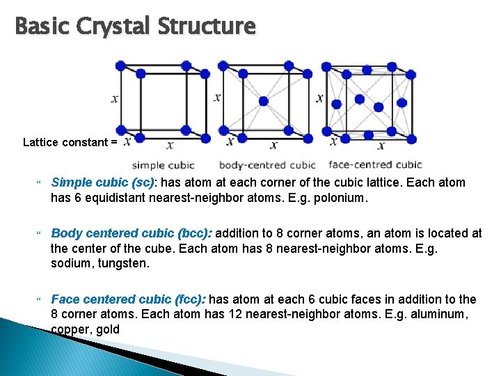
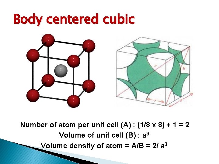
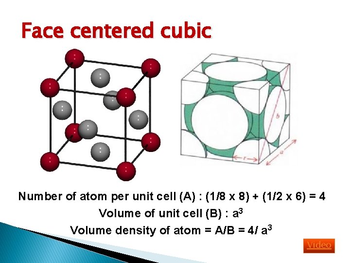
Basic Crystal Structure Lattice constant = Simple cubic (sc): has atom at each corner of the cubic lattice. Each atom has 6 equidistant nearest-neighbor atoms. E. g. polonium. Body centered cubic (bcc): addition to 8 corner atoms, an atom is located at the center of the cube. Each atom has 8 nearest-neighbor atoms. E. g. sodium, tungsten. Face centered cubic (fcc): has atom at each 6 cubic faces in addition to the 8 corner atoms. Each atom has 12 nearest-neighbor atoms. E. g. aluminum, copper, gold

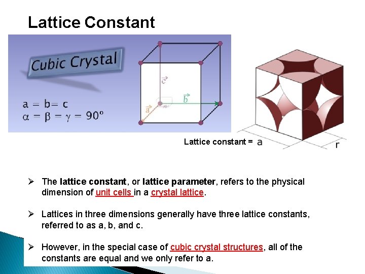
Lattice Constant Lattice constant = Ø The lattice constant, or lattice parameter, refers to the physical dimension of unit cells in a crystal lattice. Ø Lattices in three dimensions generally have three lattice constants, referred to as a, b, and c. Ø However, in the special case of cubic crystal structures, all of the constants are equal and we only refer to a.

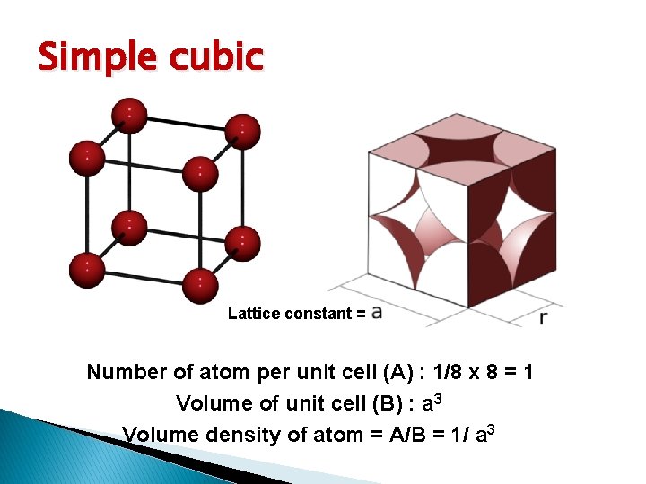
Simple cubic Lattice constant = Number of atom per unit cell (A) : 1/8 x 8 = 1 Volume of unit cell (B) : a 3 Volume density of atom = A/B = 1/ a 3

Body centered cubic Number of atom per unit cell (A) : (1/8 x 8) + 1 = 2 Volume of unit cell (B) : a 3 Volume density of atom = A/B = 2/ a 3

Face centered cubic Number of atom per unit cell (A) : (1/8 x 8) + (1/2 x 6) = 4 Volume of unit cell (B) : a 3 Volume density of atom = A/B = 4/ a 3 Video

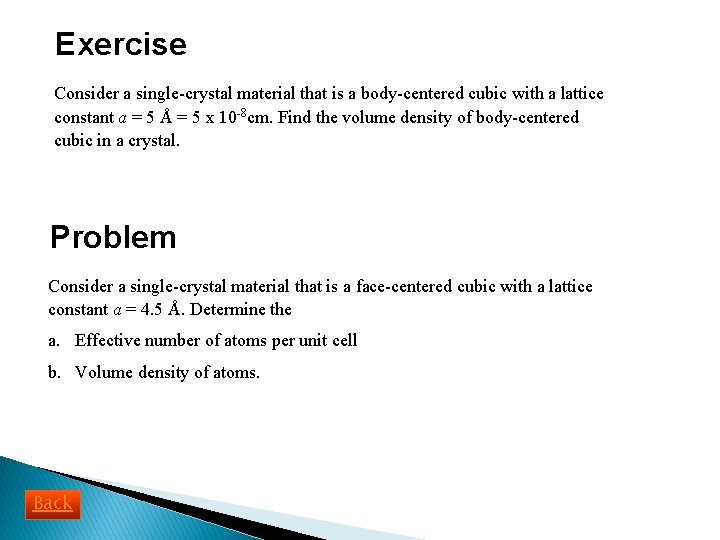
Exercise Consider a single-crystal material that is a body-centered cubic with a lattice constant a = 5 Å = 5 x 10 -8 cm. Find the volume density of body-centered cubic in a crystal. Problem Consider a single-crystal material that is a face-centered cubic with a lattice constant a = 4. 5 Å. Determine the a. Effective number of atoms per unit cell b. Volume density of atoms. Back

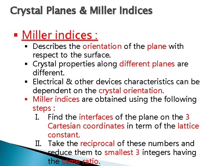
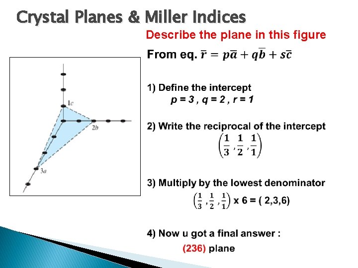
Crystal Planes & Miller Indices § Miller indices : § Describes the orientation of the plane with respect to the surface. § Crystal properties along different planes are different. § Electrical & other devices characteristics can be dependent on the crystal orientation. § Miller indices are obtained using the following steps : I. Find the interfaces of the plane on the 3 Cartesian coordinates in term of the lattice constant. II. Take the reciprocal of these numbers and reduce them to smallest 3 integers having the same ratio.

Crystal Planes & Miller Indices Describe the plane in this figure

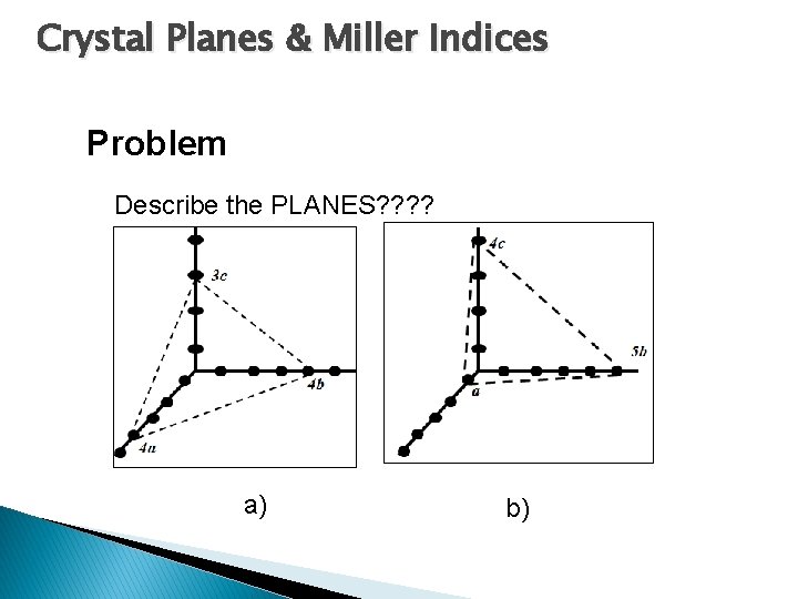
Crystal Planes & Miller Indices Problem Describe the PLANES? ? a) b)

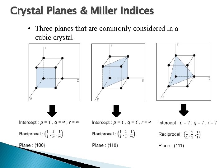
Crystal Planes & Miller Indices • Three planes that are commonly considered in a cubic crystal

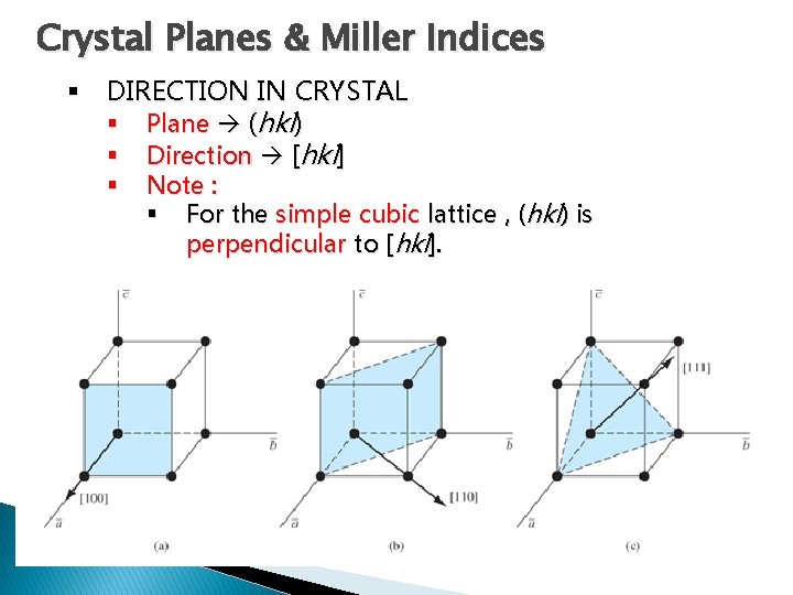
Crystal Planes & Miller Indices § DIRECTION IN CRYSTAL § Plane (hkl) § Direction [hkl] § Note : § For the simple cubic lattice , (hkl) is perpendicular to [hkl].

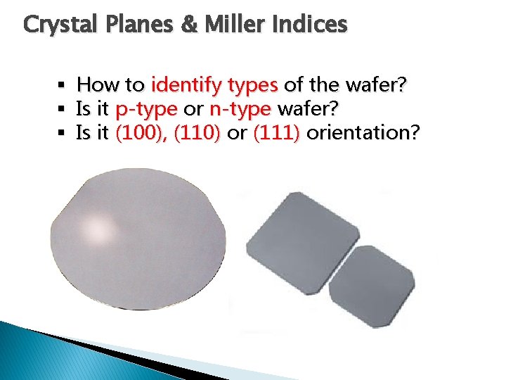
Crystal Planes & Miller Indices § How to identify types of the wafer? § Is it p-type or n-type wafer? § Is it (100), (110) or (111) orientation?

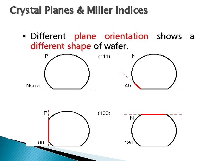
Crystal Planes & Miller Indices § Different plane orientation shows a different shape of wafer.

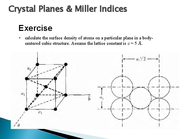
Crystal Planes & Miller Indices Exercise • calculate the surface density of atoms on a particular plane in a bodycentered cubic structure. Assume the lattice constant is a = 5 Å.

Crystal Planes & Miller Indices Problem • The lattice constant of a face-centered-cubic structure is 4. 25 Å. Calculate the surface density of atoms for a a. (100) plane b. (110) place Back

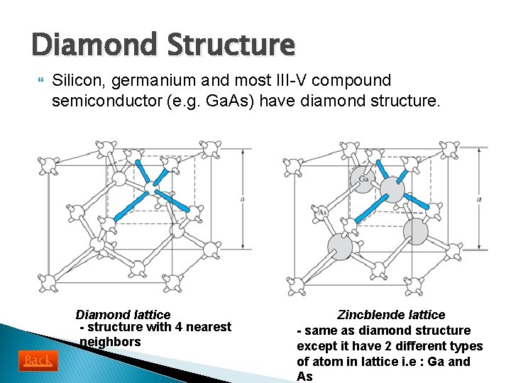
Diamond Structure Silicon, germanium and most III-V compound semiconductor (e. g. Ga. As) have diamond structure. Diamond lattice - structure with 4 nearest neighbors Back Zincblende lattice - same as diamond structure except it have 2 different types of atom in lattice i. e : Ga and As

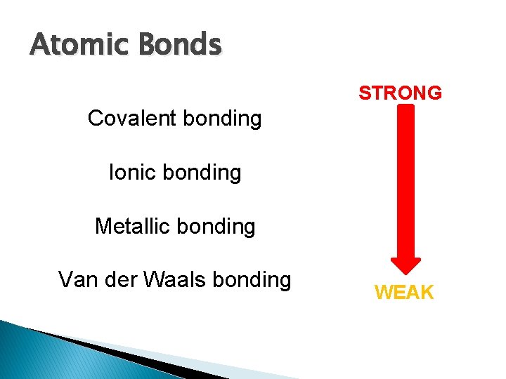
Atomic Bonds STRONG Covalent bonding Ionic bonding Metallic bonding Van der Waals bonding WEAK

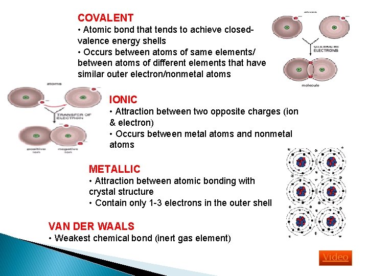
COVALENT • Atomic bond that tends to achieve closedvalence energy shells • Occurs between atoms of same elements/ between atoms of different elements that have similar outer electron/nonmetal atoms IONIC • Attraction between two opposite charges (ion & electron) • Occurs between metal atoms and nonmetal atoms METALLIC • Attraction between atomic bonding with crystal structure • Contain only 1 -3 electrons in the outer shell VAN DER WAALS • Weakest chemical bond (inert gas element) Video

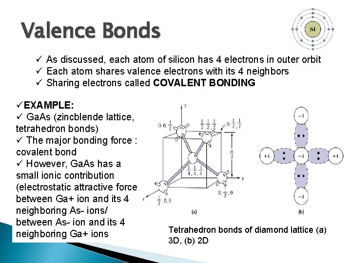
Valence Bonds ü As discussed, each atom of silicon has 4 electrons in outer orbit ü Each atom shares valence electrons with its 4 neighbors ü Sharing electrons called COVALENT BONDING üEXAMPLE: ü Ga. As (zincblende lattice, tetrahedron bonds) ü The major bonding force : covalent bond ü However, Ga. As has a small ionic contribution (electrostatic attractive force between Ga+ ion and its 4 neighboring As- ions/ between As- ion and its 4 neighboring Ga+ ions Tetrahedron bonds of diamond lattice (a) 3 D, (b) 2 D

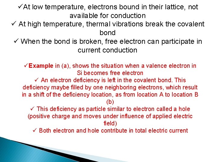
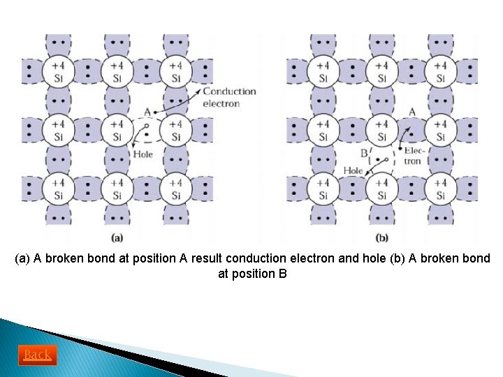
üAt low temperature, electrons bound in their lattice, not available for conduction ü At high temperature, thermal vibrations break the covalent bond ü When the bond is broken, free electron can participate in current conduction üExample in (a), shows the situation when a valence electron in Si becomes free electron ü An electron deficiency is left in the covalent bond. This deficiency maybe filled by one neighboring electrons, which result in a shift of the deficiency location, as from location A to location B (b) ü This deficiency as particle similar to electron called a hole (positive charge and moves under influence of applied electric field) ü Both electron and hole contribute in total electric current

(a) A broken bond at position A result conduction electron and hole (b) A broken bond at position B Back

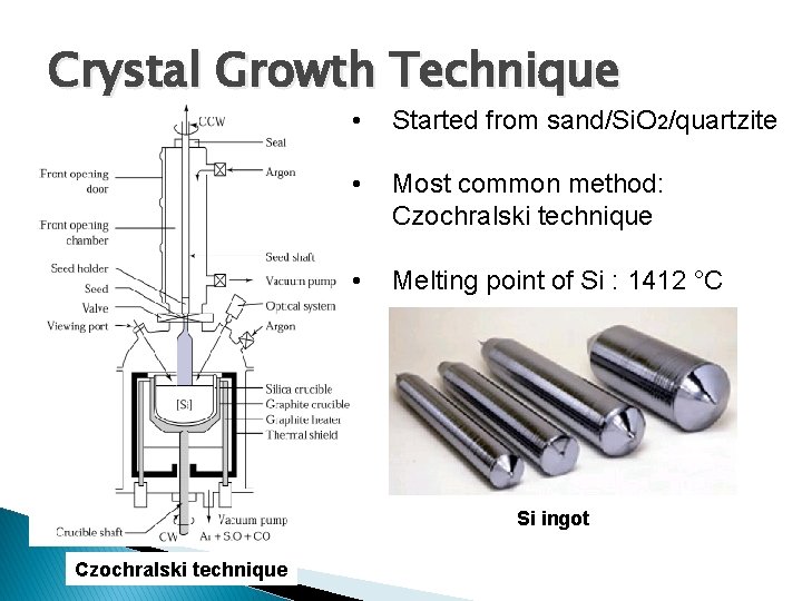
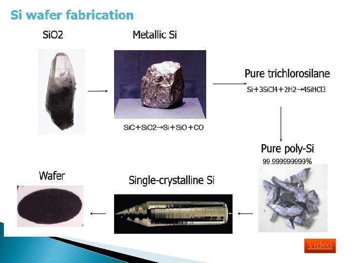
Crystal Growth Technique • Started from sand/Si. O 2/quartzite • Most common method: Czochralski technique • Melting point of Si : 1412 °C Si ingot Czochralski technique

Video