Nonhomogeneous Semiconductors Constancy of the Fermi Level at




- Slides: 65

Nonhomogeneous Semiconductors: Constancy of the Fermi Level at Equilibrium Chapter 4 Section 1 Copyright © 2016 The Mc. Graw-Hill Companies, Inc. Permission required for presentation or display

Nonhomogeneous semiconductors • So far have examined homogeneous semiconductors – Doping constant everywhere in the crystal – Material is the same everywhere (e. g. silicon) • In this chapter will look at nonhomogeneous semiconductor – Doping may vary with location – Material may vary with location • We’ll see that these can create internal electric fields that are very useful

Constancy of Fermi level at equilibrium • In a system at equilibrium, the Fermi level is constant everywhere

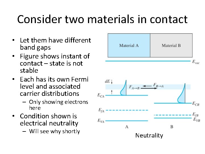
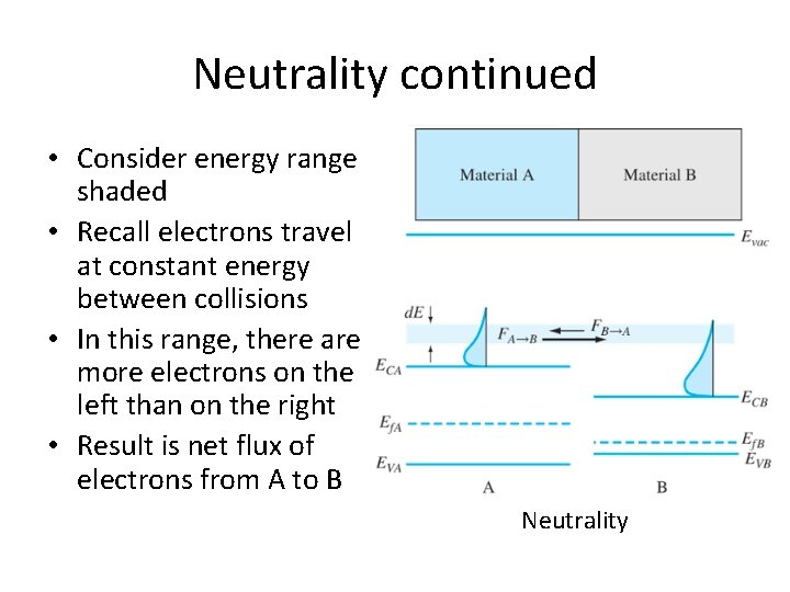
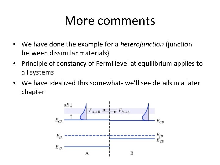
Consider two materials in contact • Let them have different band gaps • Figure shows instant of contact – state is not stable • Each has its own Fermi level and associated carrier distributions – Only showing electrons here • Condition shown is electrical neutrality – Will see why shortly Neutrality

Neutrality continued • Consider energy range shaded • Recall electrons travel at constant energy between collisions • In this range, there are more electrons on the left than on the right • Result is net flux of electrons from A to B Neutrality

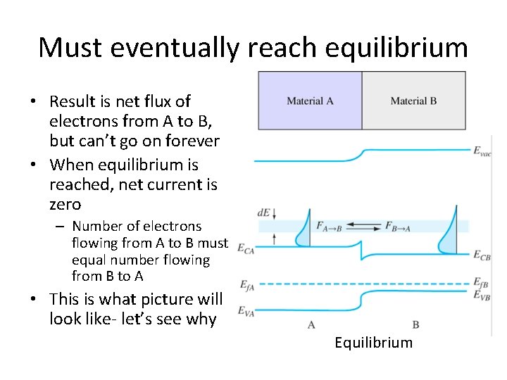
Must eventually reach equilibrium • Result is net flux of electrons from A to B, but can’t go on forever • When equilibrium is reached, net current is zero – Number of electrons flowing from A to B must equal number flowing from B to A • This is what picture will look like- let’s see why Equilibrium

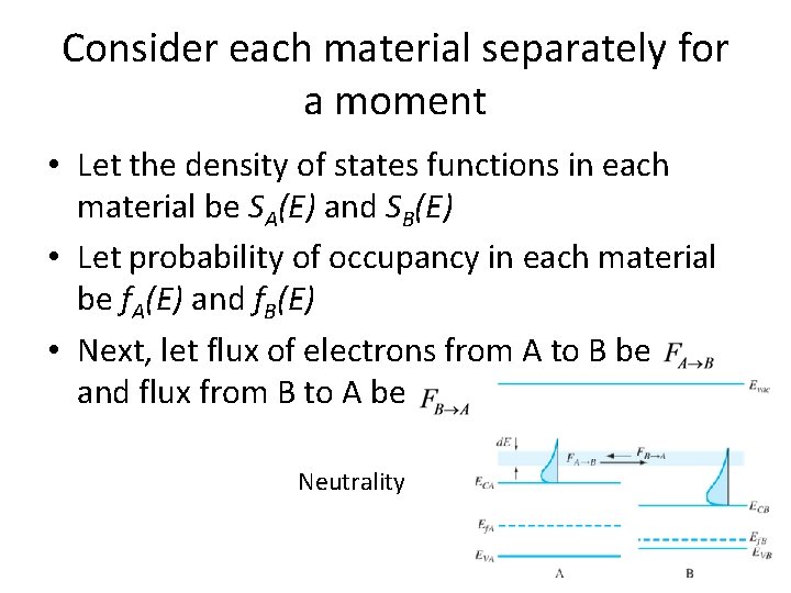
Consider each material separately for a moment • Let the density of states functions in each material be SA(E) and SB(E) • Let probability of occupancy in each material be f. A(E) and f. B(E) • Next, let flux of electrons from A to B be and flux from B to A be Neutrality

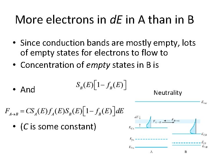
More electrons in d. E in A than in B • Since conduction bands are mostly empty, lots of empty states for electrons to flow to • Concentration of empty states in B is • And • (C is some constant) Neutrality

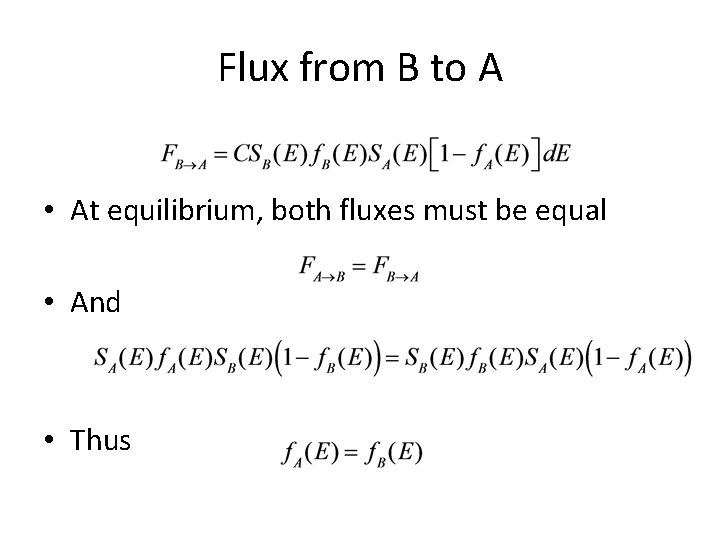
Flux from B to A • At equilibrium, both fluxes must be equal • And • Thus

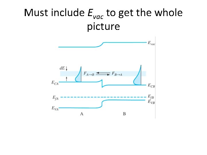
Must include Evac to get the whole picture

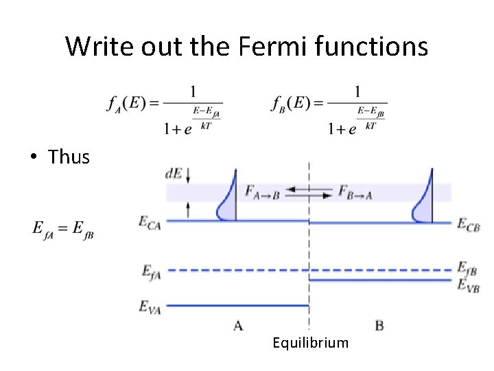
Write out the Fermi functions • Thus Equilibrium

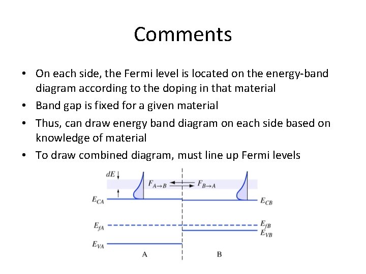
Comments • On each side, the Fermi level is located on the energy-band diagram according to the doping in that material • Band gap is fixed for a given material • Thus, can draw energy band diagram on each side based on knowledge of material • To draw combined diagram, must line up Fermi levels

More comments • We have done the example for a heterojunction (junction between dissimilar materials) • Principle of constancy of Fermi level at equilibrium applies to all systems • We have idealized this somewhat- we’ll see details in a later chapter

Key points • In a system at equilibrium, the Fermi level is constant everywhere • Next section: what happens when the doping concentration varies with position?

Graded Doping Chapter 4 Section 2 Copyright © 2016 The Mc. Graw-Hill Companies, Inc. Permission required for presentation or display

Introduction • In last section we combined two materials with different band gaps • Here, will consider a single material but let the doping vary with position

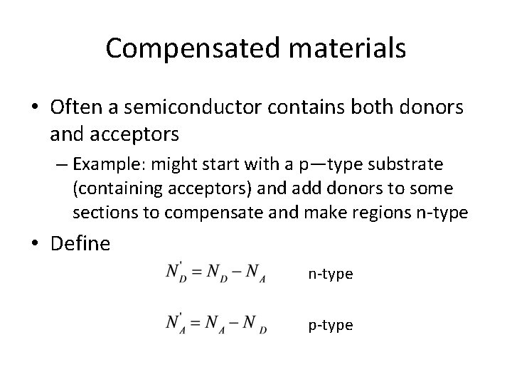
Compensated materials • Often a semiconductor contains both donors and acceptors – Example: might start with a p—type substrate (containing acceptors) and add donors to some sections to compensate and make regions n-type • Define n-type p-type

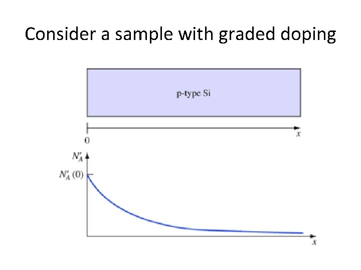
Consider a sample with graded doping

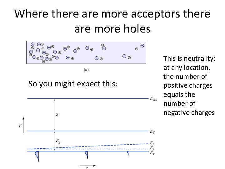
Where there are more acceptors there are more holes So you might expect this: This is neutrality: at any location, the number of positive charges equals the number of negative charges

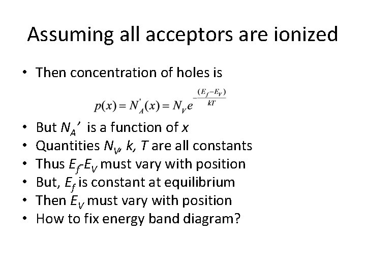
Assuming all acceptors are ionized • Then concentration of holes is • • • But NA’ is a function of x Quantities NV, k, T are all constants Thus Ef-EV must vary with position But, Ef is constant at equilibrium Then EV must vary with position How to fix energy band diagram?

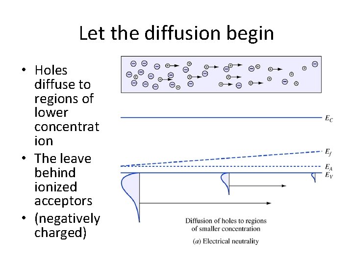
Let the diffusion begin • Holes diffuse to regions of lower concentrat ion • The leave behind ionized acceptors • (negatively charged)

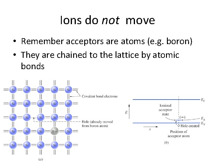
Ions do not move • Remember acceptors are atoms (e. g. boron) • They are chained to the lattice by atomic bonds

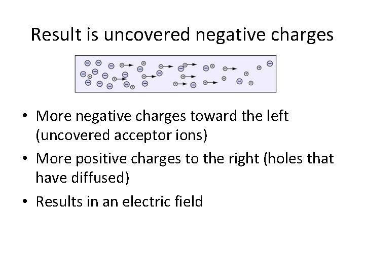
Result is uncovered negative charges • More negative charges toward the left (uncovered acceptor ions) • More positive charges to the right (holes that have diffused) • Results in an electric field

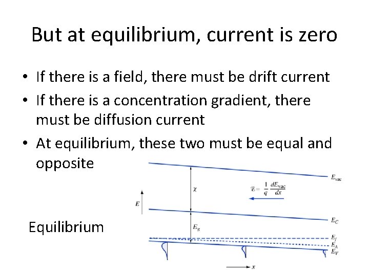
But at equilibrium, current is zero • If there is a field, there must be drift current • If there is a concentration gradient, there must be diffusion current • At equilibrium, these two must be equal and opposite Equilibrium

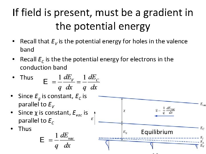
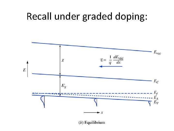
If field is present, must be a gradient in the potential energy • Recall that EV is the potential energy for holes in the valence band • Recall EC is the potential energy for electrons in the conduction band • Thus • Since Eg is constant, EC is parallel to EV • Since χ is constant, Evac is parallel to EC • Thus Equilibrium

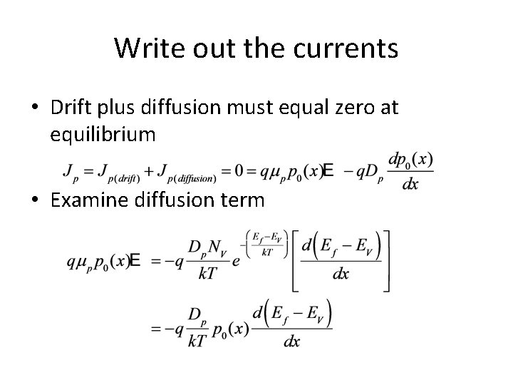
Write out the currents • Drift plus diffusion must equal zero at equilibrium • Examine diffusion term

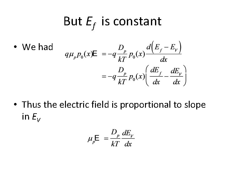
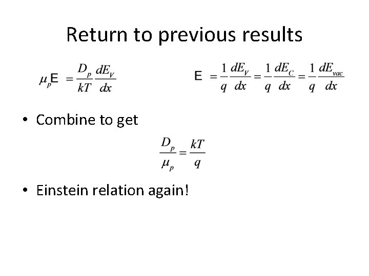
But Ef is constant • We had • Thus the electric field is proportional to slope in EV

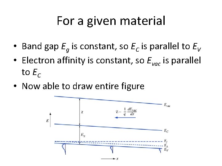
For a given material • Band gap Eg is constant, so EC is parallel to EV • Electron affinity is constant, so Evac is parallel to EC • Now able to draw entire figure

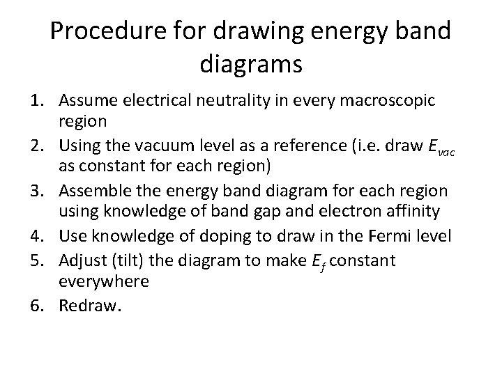
Procedure for drawing energy band diagrams 1. Assume electrical neutrality in every macroscopic region 2. Using the vacuum level as a reference (i. e. draw Evac as constant for each region) 3. Assemble the energy band diagram for each region using knowledge of band gap and electron affinity 4. Use knowledge of doping to draw in the Fermi level 5. Adjust (tilt) the diagram to make Ef constant everywhere 6. Redraw.

Return to previous results • Combine to get • Einstein relation again!

Recall under graded doping:

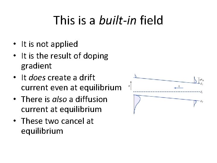
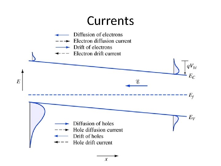
This is a built-in field • It is not applied • It is the result of doping gradient • It does create a drift current even at equilibrium • There is also a diffusion current at equilibrium • These two cancel at equilibrium

Currents

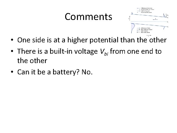
Comments • One side is at a higher potential than the other • There is a built-in voltage Vbi from one end to the other • Can it be a battery? No.

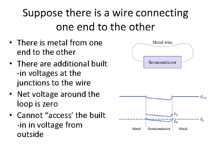
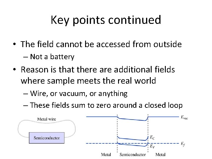
Suppose there is a wire connecting one end to the other • There is metal from one end to the other • There additional built -in voltages at the junctions to the wire • Net voltage around the loop is zero • Cannot “access’ the built -in in voltage from outside

Key points • If the doping varies with position, there is a change in carrier concentration – Sets up a diffusion current • As carriers (charged) diffuse, they leave “uncovered” ionized donors or acceptors – Donors and acceptors cannot move! • The charges set up an electric field • Electric field causes a gradient in the potential energy (band edges) • The electric field causes drift, which exactly compensates the diffusion • Both drift and diffusion going on all the time, even at equilibrium- but they cancel

Key points, continued • Varying the doping concentration creates built-in internal electric fields • Fields create drift currents • Varying doping creates diffusion currents • At equilibrium, these cancel – For both electrons and holes • There additional built-in fields at contacts to sample, so is not a battery

Nonuniform Composition Chapter 4 Section 3 Copyright © 2016 The Mc. Graw-Hill Companies, Inc. Permission required for presentation or display

Introduction • We saw that nonuniform doping in a material created built-in internal electric fields – Band gaps, electron affinities were constant but doping caused band edges to slope • Now we will examine what happens if the material is not uniform – Band gap not uniform- what happens?

Consider a graded alloy • Let the sample be pure silicon at one end • Let germanium be introduced in increasing amounts along sample – Results in alloy of Siy. Ge 1 -y – Variable y denotes fraction of Si • Both Si and Ge are in column four – Will bond covalently – Have same crystal structure • But they have different band gaps

Let the material be doped • Let’s say acceptors • Say doped such that Ef is same distance from EV throughout • Doping is not quite uniform because Si and Si. Ge alloys will have different slightly NV (because of different effective masses)

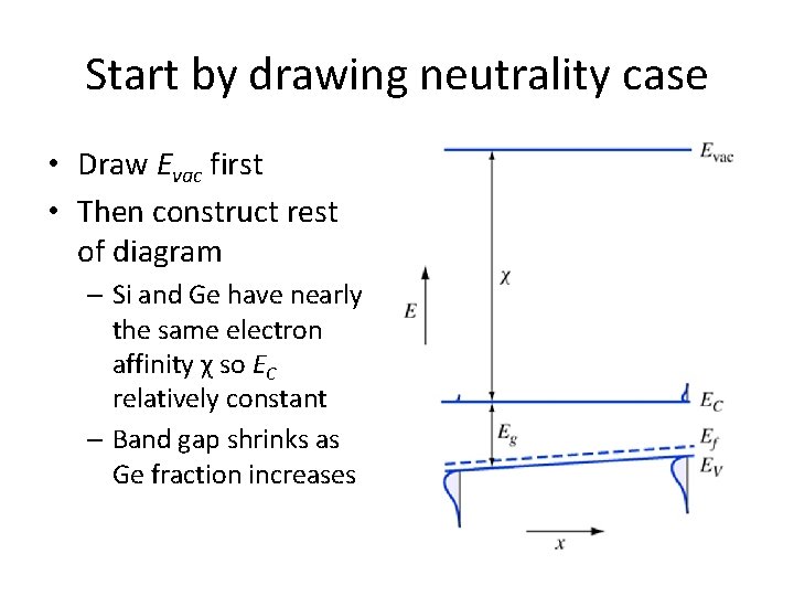
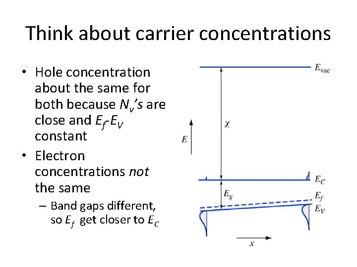
Start by drawing neutrality case • Draw Evac first • Then construct rest of diagram – Si and Ge have nearly the same electron affinity χ so EC relatively constant – Band gap shrinks as Ge fraction increases

Think about carrier concentrations • Hole concentration about the same for both because Nv’s are close and Ef-EV constant • Electron concentrations not the same – Band gaps different, so Ef get closer to EC

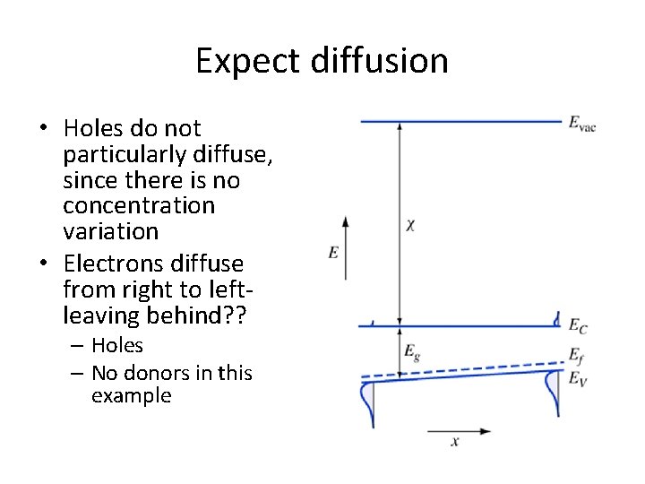
Expect diffusion • Holes do not particularly diffuse, since there is no concentration variation • Electrons diffuse from right to leftleaving behind? ? – Holes – No donors in this example

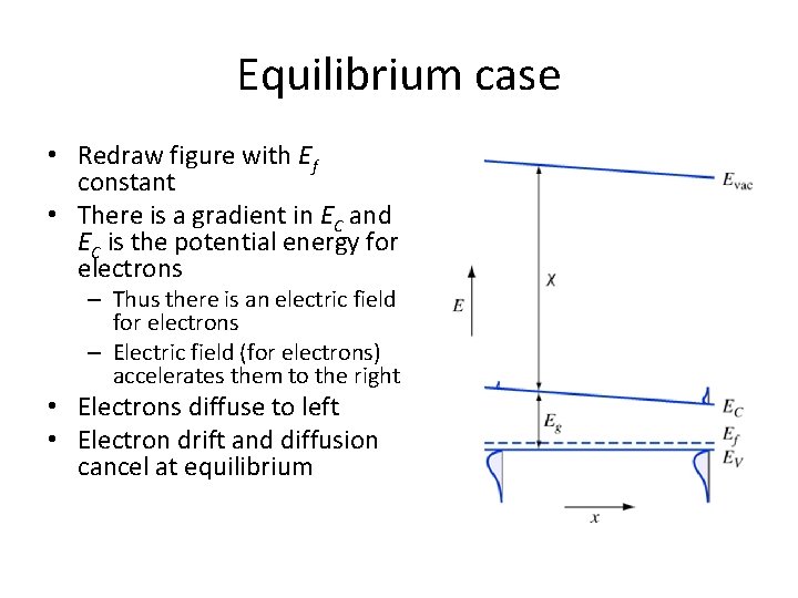
Equilibrium case • Redraw figure with Ef constant • There is a gradient in EC and EC is the potential energy for electrons – Thus there is an electric field for electrons – Electric field (for electrons) accelerates them to the right • Electrons diffuse to left • Electron drift and diffusion cancel at equilibrium

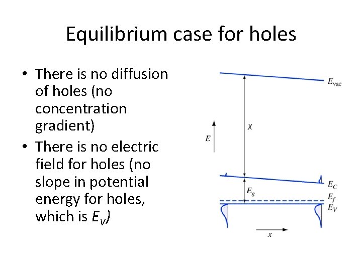
Equilibrium case for holes • There is no diffusion of holes (no concentration gradient) • There is no electric field for holes (no slope in potential energy for holes, which is EV)

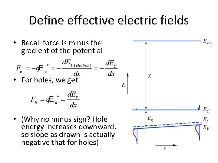
Define effective electric fields • Recall force is minus the gradient of the potential • For holes, we get • (Why no minus sign? Hole energy increases downward, so slope as drawn is actually negative that for holes)

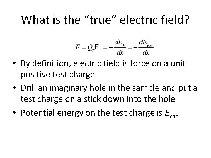
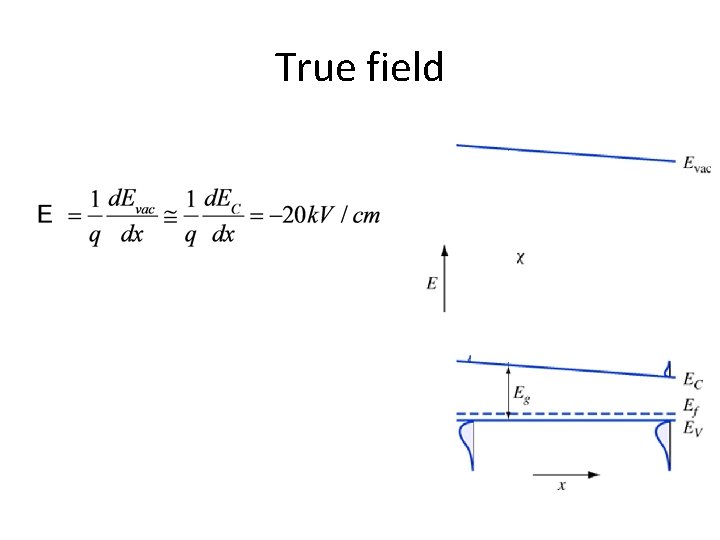
What is the “true” electric field? • By definition, electric field is force on a unit positive test charge • Drill an imaginary hole in the sample and put a test charge on a stick down into the hole • Potential energy on the test charge is Evac

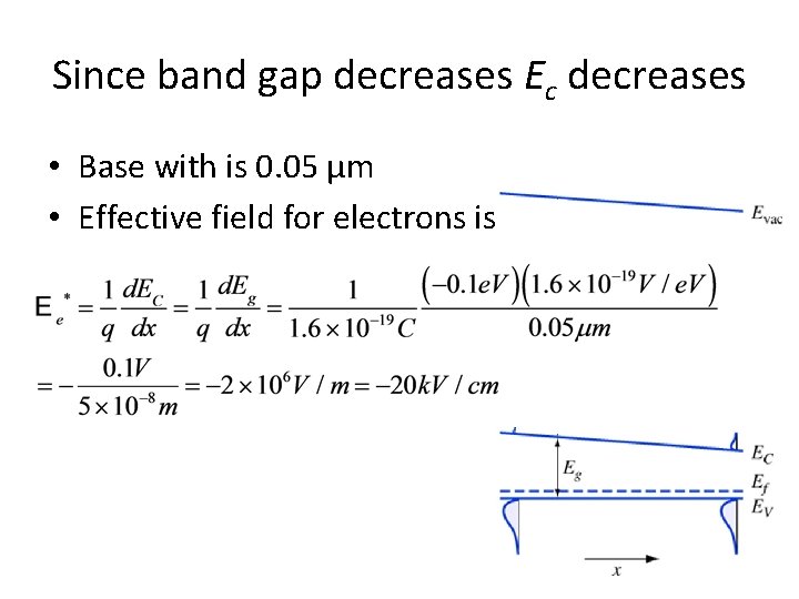
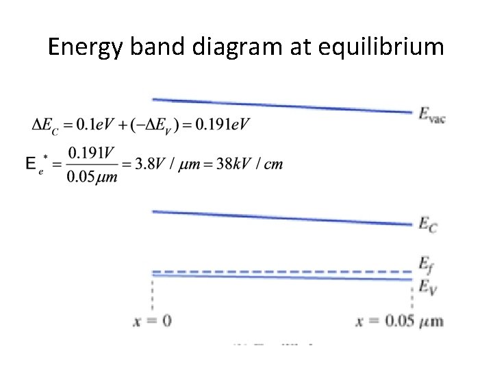
Example • Consider a transistor with a Si: Ge base in which the band gap varies linearly by 0. 1 e. V across the 0. 05 µm base width. Assume that the net acceptor concentration is constant. Find the effective electric field and force for holes and electrons, and the true electric field.

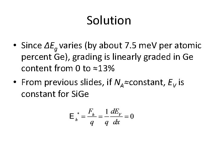
Solution • Since ΔEg varies (by about 7. 5 me. V per atomic percent Ge), grading is linearly graded in Ge content from 0 to ≈13% • From previous slides, if NA≈constant, EV is constant for Si. Ge

Since band gap decreases Ec decreases • Base with is 0. 05 µm • Effective field for electrons is

True field

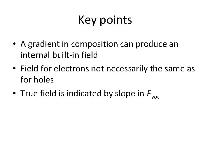
Key points • A gradient in composition can produce an internal built-in field • Field for electrons not necessarily the same as for holes • True field is indicated by slope in Evac

Graded Doping and Nonuniform Composition Combined Chapter 4 Section 4 Copyright © 2016 The Mc. Graw-Hill Companies, Inc. Permission required for presentation or display

Introduction • In an actual Si. Ge transistor base may have both composition gradients and doping gradient • Effect is to speed up transistor even more – Higher operating frequencies

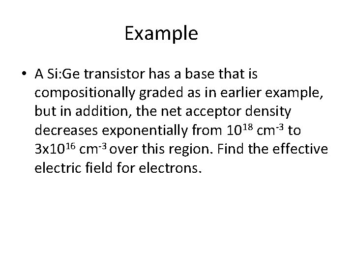
Example • A Si: Ge transistor has a base that is compositionally graded as in earlier example, but in addition, the net acceptor density decreases exponentially from 1018 cm-3 to 3 x 1016 cm-3 over this region. Find the effective electric field for electrons.

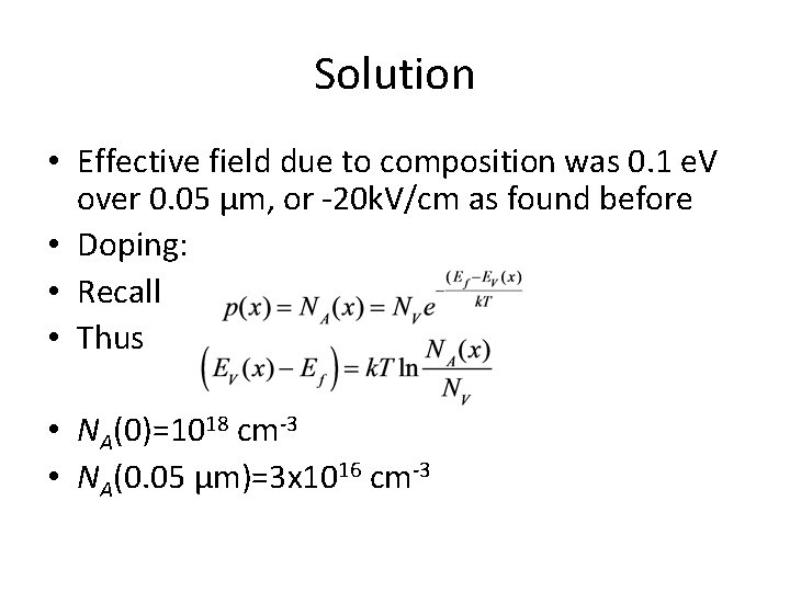
Solution • Effective field due to composition was 0. 1 e. V over 0. 05 µm, or -20 k. V/cm as found before • Doping: • Recall • Thus • NA(0)=1018 cm-3 • NA(0. 05 µm)=3 x 1016 cm-3

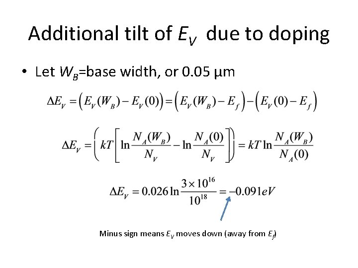
Additional tilt of EV due to doping • Let WB=base width, or 0. 05 µm Minus sign means EV moves down (away from Ef)

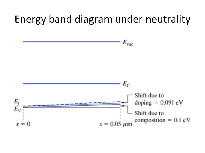
Energy band diagram under neutrality

Energy band diagram at equilibrium

Key points • Both doping gradients and compositional variations can be used to create internal, builtin electric fields • These can be combined to increase the effect • Effective fields for electrons may be different from those for holes

Summary Chapter 4 Section 5 Copyright © 2016 The Mc. Graw-Hill Companies, Inc. Permission required for presentation or display

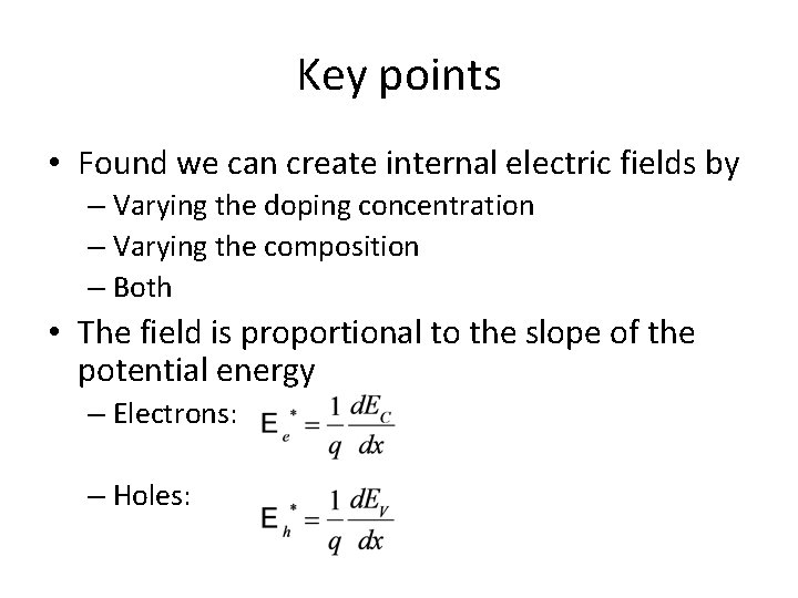
Key points • Found we can create internal electric fields by – Varying the doping concentration – Varying the composition – Both • The field is proportional to the slope of the potential energy – Electrons: – Holes:

Key points continued • The field cannot be accessed from outside – Not a battery • Reason is that there additional fields where sample meets the real world – Wire, or vacuum, or anything – These fields sum to zero around a closed loop

Road map • Real semiconductor devices are usually made of combinations of n-type and p-type materials, joined – Example: a diode can be made from a junction between an n-type region and a p-type region • The internal fields will have some very interesting effects • Next up: Part 2 Diodes