Welcome to EE 130230 A Integrated Circuit Devices

- Slides: 11

Welcome to EE 130/230 A Integrated Circuit Devices Instructors: Prof. Tsu-Jae King Liu (tsujae@berkeley. edu) TA: Peng Zheng (pzheng@eecs. berkeley. edu) Web page: http: //www-inst. eecs. berkeley. edu/~ee 130/ b. Space: EE 130/230 A Fall 2013 Piazza: https: //piazza. com/berkeley/fall 2013/ee 130230 a/home Objectives: • Fundamental understanding of the working principles of semiconductor devices used in modern ICs. • An ability to design a transistor to meet performance requirements within realistic constraints.

Schedule • Lectures (241 Cory): Tu. Th 2 -3: 30 PM • Discussion Section (beginning Tuesday 9/3): – Section 101 (247 Cory): Mo 10 -11 AM – Section 102 (247 Cory): We 12 -1 PM • Office Hours: – Prof. Liu (225 Cory): – Peng Zheng (288 Cory): EE 130/230 A Fall 2013 Mo 4 -5 PM Tu 9 -10 AM and We 4 -5 PM Course Overview, Slide 2

Relation to Other Courses • Prerequisite: – EECS 40: Basic properties of semiconductors; basic understanding of transistor operation – Familiarity with the Bohr atomic model • Relation to other courses: – EE 230 A is prerequisite for EE 230 B (Solid State Devices) – EE 130 is also helpful (but not required) for IC analysis and design courses such as EE 140 and EE 141, as well as for the microfabrication technology course EE 143 EE 130/230 A Fall 2013 Course Overview, Slide 3

Reading Material • Textbook: Semiconductor Device Fundamentals by R. F. Pierret (Addison Wesley, 1996) • Reference: – Modern Semiconductor Devices for Integrated Circuits by C. Hu (Prentice Hall, 2009) EE 130/230 A Fall 2013 Course Overview, Slide 4

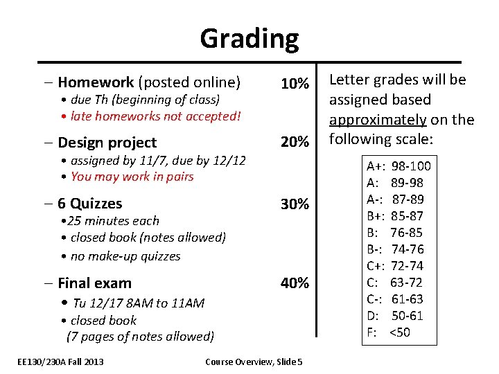
Grading – Homework (posted online) 10% – Design project 20% • due Th (beginning of class) • late homeworks not accepted! • assigned by 11/7, due by 12/12 • You may work in pairs – 6 Quizzes 30% – Final exam • Tu 12/17 8 AM to 11 AM 40% • 25 minutes each • closed book (notes allowed) • no make-up quizzes • closed book (7 pages of notes allowed) EE 130/230 A Fall 2013 Course Overview, Slide 5 Letter grades will be assigned based approximately on the following scale: A+: 98 -100 A: 89 -98 A-: 87 -89 B+: 85 -87 B: 76 -85 B-: 74 -76 C+: 72 -74 C: 63 -72 C-: 61 -63 D: 50 -61 F: <50

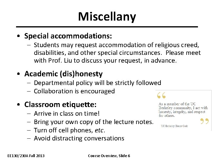
Miscellany • Special accommodations: – Students may request accommodation of religious creed, disabilities, and other special circumstances. Please meet with Prof. Liu to discuss your request, in advance. • Academic (dis)honesty – Departmental policy will be strictly followed – Collaboration is encouraged • Classroom etiquette: – – Arrive in class on time! Bring your own copy of the lecture notes. Turn off cell phones, etc. Avoid distracting conversations EE 130/230 A Fall 2013 Course Overview, Slide 6

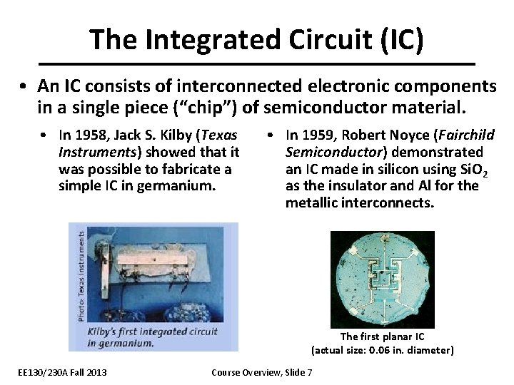
The Integrated Circuit (IC) • An IC consists of interconnected electronic components in a single piece (“chip”) of semiconductor material. • In 1958, Jack S. Kilby (Texas Instruments) showed that it was possible to fabricate a simple IC in germanium. • In 1959, Robert Noyce (Fairchild Semiconductor) demonstrated an IC made in silicon using Si. O 2 as the insulator and Al for the metallic interconnects. The first planar IC (actual size: 0. 06 in. diameter) EE 130/230 A Fall 2013 Course Overview, Slide 7

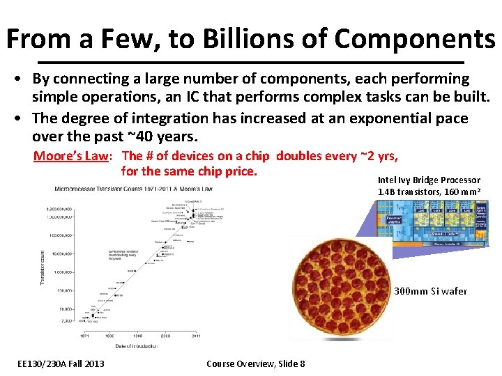
From a Few, to Billions of Components • By connecting a large number of components, each performing simple operations, an IC that performs complex tasks can be built. • The degree of integration has increased at an exponential pace over the past ~40 years. Moore’s Law: The # of devices on a chip doubles every ~2 yrs, for the same chip price. Intel Ivy Bridge Processor 1. 4 B transistors, 160 mm 2 300 mm Si wafer EE 130/230 A Fall 2013 Course Overview, Slide 8

Impact of Moore’s Law http: //www. morganstanley. com/institutional/techresearch/pdfs/2 SETUP_12142009_RI. pdf # DEVICES (MM) Transistor Scaling Higher Performance, Investment Lower Cost Market Growth CMOS generation: 1 um • • 180 nm • • 22 nm YEAR EE 130/230 A Fall 2013 Course Overview, Slide 9

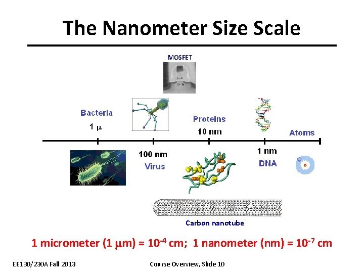
The Nanometer Size Scale MOSFET Carbon nanotube 1 micrometer (1 mm) = 10 -4 cm; 1 nanometer (nm) = 10 -7 cm EE 130/230 A Fall 2013 Course Overview, Slide 10

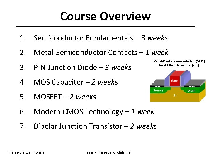
Course Overview 1. Semiconductor Fundamentals – 3 weeks 2. Metal-Semiconductor Contacts – 1 week 3. P-N Junction Diode – 3 weeks Metal-Oxide-Semiconductor (MOS) Field-Effect Transistor (FET) 4. MOS Capacitor – 2 weeks 5. MOSFET – 2 weeks 6. Modern CMOS Technology – 1 week 7. Bipolar Junction Transistor – 2 weeks EE 130/230 A Fall 2013 Course Overview, Slide 11