EMT 248 Design 8085 Microprocessor System Semester II


 and data are stored Ø Organized")


 A 13 A 14")


- Slides: 54
EMT 248: Design 8085 Microprocessor System Semester II 2013/14 School of Microelectronic Engineering Universiti Malaysia Perlis
Outline Ø Ø Ø Bus organization Address/Data Bus Control Bus Memory and I/O Address Decoders I/O Mapping
Bus Organization
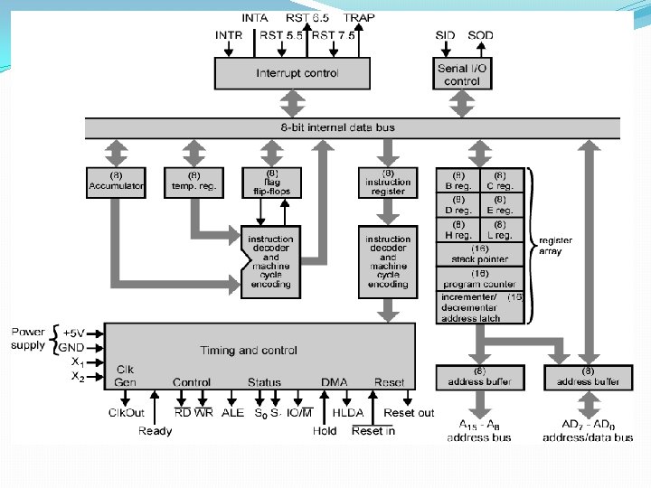
8085 CPU
8085 Microprocessor System Block Diagram
Example Block Diagram Address Bus 8085 Data Bus Control Bus Interface Memory
What is an Interface? Ø an interface is a concept that refers to a point of interaction between components, and is applicable at the level of both hardware and software. Ø This allows a component, (such as a graphics card or an Internet browser), to function independently while using interfaces to communicate with other components via an input/output system and an associated protocol.
8085 Interfacing Pins Higher Address Bus Lower Address/Data Bus 8085 ALE Control Bus A 15 – A 8 AD 7 – AD 0
The 8085 Bus Structure Ø Consists of 16 address lines: A 0 – A 15 Ø Operates in unidirectional mode: The address bits are always sent from the MPU to peripheral devices, not reverse. Ø 16 address lines are capable of addressing a total of 216 = 65, 536 (64 k) memory locations. Ø Address locations: 0000 (hex) – FFFF (hex)
The 8085 Bus Structure Data Bus Ø Consists of 8 data lines: D 0 – D 7 Ø Operates in bidirectional mode: The data bits are sent from the MPU to peripheral devices, as well as from the peripheral devices to the MPU. Higher-order Address Lower-order Address A 15 A 14 A 13 A 12 A 11 A 10 A 9 A 8 AD 7 AD 6 AD 5 AD 4 AD 3 AD 2 AD 1 AD 0 Data Bus
The 8085 Bus Structure Control Bus Ø Comprised of various signal lines that carry synchronization signals Ø The MPU use such lines to perform the third function: providing timing signals Ø A group of signal includes: § two control signals (RD/ and WR/) § Three status signals ( ) to identify the nature of the operation, § One special signal (ALE) to indicate the beginning of the operation.
Address/Data Bus
Higher Order Address Bus Ø The higher order address bus is a unidirectinal bus. Ø It carries most significant 8 -bits of a 16 -bit address of memory or I/O device. Ø Address remains on lines as long operation is not completed.
Lower Order Address/Data Bus Ø This bus is bidirectional and works on time division multiplexing between address and data. Ø During first clock cycle, it serves as a least significant 8 -bits of memory/ IO address. Ø For second and third clock cycles it acts as data bus and carries data.
Question How the processor knows the Lower Order bits is for Address or Data? Demultiplexing (DEMUX)
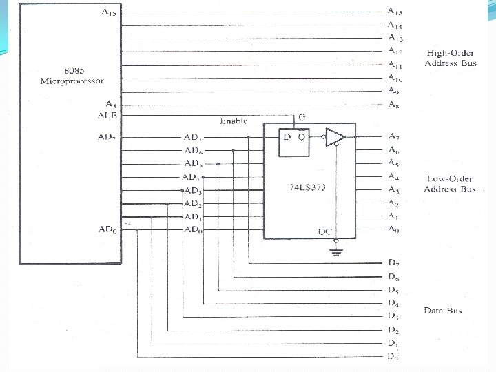
Demultiplexing § A hardware register provided by the system designer to save the contents of the data bus and low order address lines. § 8085 microprocessor commonly uses latch to demultiplex the address and data bus. § The most widely used latch for demultiplexing is 74 LS 373 IC. § separation of address/data bus AD 0 -AD 7 into address bus A 7—A 0 and data bus D 7—D 0. § The data bus and low order address lines are multiplexed in order to save pin count.
How the Latch / Demultiplexer is Function? § 1 st clock cycle, • lower address is transferred on AD 0— AD 7. • ALE is high and latch is enabled. • Address available at A 0 —A 7. § 2 nd and 3 rd clock cycle • ALE goes low and latch is disabled. • ADo—AD 7 will act as D 0—D 7.
Multiplexing § A method by which multiple digital data streams are combined into one signal over a shared medium. § Lower order address bus & Data bus are on the 8085 microprocessor multiplexed on same lines i. e. AD 0 to AD 7 and A 8 to A 15.
74 LS 373
Control Bus
8085 Machine Cycle Status and Control Signal
8085 Machine Cycle Status and Control Signal
Memory and I/O
Memory and I/O Memory Ø Where instructions (programs) and data are stored Ø Organized in arrays of locations (addresses), each storing one byte (8 bits) in general Ø A read operation to a particular location always returns the last value stored in that location. Ø The memory is made up of semiconductor material used to store the programs and data. The types of memory is, Ø Primary or main memory - RAM and ROM Ø storing a program temporarily (commonly called loading) and executing a program. Ø speed of this type of memory should be fast.
Memory and I/O Ø Secondary memory - Floppy, Hard Disk and CD-ROM Ø used for bulk storage of data and information Ø Slower and Sequential Access Nature. Ø non-volatile nature. I/O devices Ø Enable system to interact with the world Ø The MPU views the I/O device registers just like memory that can be accessed over the bus. However, I/O registers are connected to external wires, device control logic, etc. Ø The MPU accepts binary data as input from devices (keyboards and Analog To Digital (A/D) converters) and sends the data to output devices (LEDs and printer)
Address Decoders
Memory Chip ‘k’ data input lines ‘n’ address lines read write Memory Chip select 2 n words ‘k’ bits per word ‘k’ data output lines
Interface with two memory chips A 1 A 0 11 11 10 10 01 01 00 00 Memory 1 Memory 2
Interface with two memory chips A 1 A 0 A 2 11 011 11 10 010 10 110 01 01 101 00 00 100 Memory 1 Memory 2
Interface with Multiple Chips Ø In case of multiple chips, simple circuit like NOT gate will not work. Ø In this case normally decoder circuits like 3 -to-8 decoder circuit 74 LS 138 are used. Ø These circuit are called address decoders.
Interface with Multiple Chips Ø Using random logic - Using logic gates such as AND, OR, NOT and etc. Ø Using M-Line to N-Line Decoder - Use existing general decoders such as 74 LS 138, 74 LS 154 and etc. Ø Using PAL or FPGA - Using Programmable logic array devices such as PAL 22 V 10 , PAL 16 L 8 or Field Programmable Gate Array, i. e. XILINK.
Example ROM & RAM Size Ø ROM size 8 K x 8 bit 13 bit address line A 0 - A 12 213 = 8192 (0000 H - 1 FFFH) Ø RAM size 8 K x 8 bit 13 bit address line A 0 - A 12 213 = 8192 (0000 H - 1 FFFH)
Memory Map 0000 H 1 FFFH 2000 H 3 FFFH 4000 H ROM RAM Not Used FFFFH 1 FFFH 2000 H 3 FFFH 4000 H OR RAM ROM Not Used FFFFH
Address Decoding ROM RAM Note: A 15. . A 12 0000 0001 0010 0011 A 11. . A 8 0000 1111 A 7. . A 4 0000 1111 A 3. . A 0 0000 1111 ROM A 13 = 0 , RAM A 13 = 1 Memory access, signal IO/M = 0
Memory Decoding Using Random Logic A 15 A 14 A 13 OR ROM CS RAM CS
Memory Decoding Using 3 to 8 Decoder (74 LS 138) A 13 A 14 A 15 ROM CS +5 V IO/M GND RAM CS
Truth Table 74 LS 138 INPUT C B A G 1 G 2 A G 2 B X X X 0 0 1 1 X X X 0 1 0 1 0 1 1 1 1 1 X 1 0 0 0 0 0 X X 1 0 0 0 0 Y 0 Y 1 Y 2 1 1 1 1 1 0 1 1 1 1 OUTPUT Y 3 Y 4 1 1 1 0 1 1 1 1 Y 5 Y 6 Y 7 1 1 1 1 1 1 0 1 1 1 0
Types of Address Decoding Ø There are two types of address decoding techniques § Exhaustive Decoding § Partial Decoding
Exhaustive Decoding Ø In this type of scheme all the 16 bits of the 8085 address bus are used to select a particular location in memory chip. Ø Advantages: § Complete Address Utilization § Ease in Future Expansion § No Bus Contention, as all addresses are unique. Ø Disadvantages § Increased hardware and cost. § Speed is less due to increased delay.
Partial Decoding Ø In this scheme minimum number of address lines are used as required to select a memory location in chip. Ø Advantages: § Simple, Cheap and Fast. Ø Disadvantages: § Unutilized space & fold back (multiple mapping). § Bus Contention. § Difficult future expansion.
I/O Mapping
Interfacing I/O Devices Ø Using I/O devices data can be transferred between the microprocessor and the outside world. Ø This can be done in groups of 8 bits using the entire data bus. This is called parallel I/O. Ø The other method is serial I/O where one bit is transferred at a time using the SID and SOD pins on the Microprocessor.
Types of Parallel Interface Ø There are two ways to interface 8085 with I/O devices in parallel data transfer mode: Ø Memory Mapped I/O Ø I/O Mapped I/O
Memory Mapped I/O Ø It considers them like any other memory location. Ø They are assigned a 16 -bit address within the address range of the 8085. Ø The exchange of data with these devices follows the transfer of data with memory. The user uses the same instructions used for memory.
I/O Mapped I/O Ø It treats them separately from memory. Ø I/O devices are assigned a “port number” within the 8 -bit address range of 00 H to FFH. Ø The user in this case would access these devices using the IN and OUT instructions only.
I/O Mapped I/O Ø Memory Mapped I/O Ø I/O Mapped I/O �I/O is treated as memory. �I/O is treated I/O. � 16 -bit addressing. � 8 - bit addressing. �More Decoder Hardware. �Less Decoder �Can address 216=64 k locations. �Less memory is available Hardware. �Can address 28=256 locations. �Whole memory address space is available.
I/O mapped I/O Vs Memory Mapped I/O Ø Memory Mapped I/O �Memory Instructions are used. �Memory control signals are used. �Arithmetic and logic operations can be performed on data. �Data transfer b/w register and IO. Ø I/O Mapped I/O �Special Instructions are used like IN, OUT. �Special control signals are used. �Arithmetic and logic operations can not be performed on data. �Data transfer b/w accumulator and IO.
The interfacing of output devices Ø Output devices are usually slow. Ø Also, the output is usually expected to continue appearing on the output device for a long period of time. Ø Given that the data will only be present on the data lines for a very short period (microseconds), it has to be latched externally.
The interfacing of output devices Ø To do this, the external latch should be enabled when the port’s address is present on the address bus, the IO/M signal is set high and WR is set low. Ø The resulting signal would be active when the output device is being accessed by the microprocessor. Ø Decoding the address bus (for memorymapped devices) follows the same techniques discussed in interfacing memory.
The interfacing of Input devices Ø The basic concepts are similar to interfacing of output devices. Ø The address lines are decoded to generate a signal that is active when the particular port is being accessed. Ø An IO/RD signal is generated by combining the IO/M and the RD signals from the microprocessor.
The interfacing of Input devices Ø A tri-state buffer is used to connect the input device to the data bus. Ø The control (Enable) for these buffers is connected to the result of combining the address signal and the signal IO/RD.
Thank you Q&A