Chapter 16 MOS Fundamental Semiconductor Device Fundamentals Chapter

- Slides: 50

Chapter 16. MOS Fundamental Semiconductor Device Fundamentals Chapter 16. MOS FUNDAMENTALS Sung June Kim kimsj@snu. ac. kr http: //nanobio. snu. ac. kr Bioelectronic & Systems Lab.

Chapter 16. MOS Fundamental Semiconductor Device Fundamentals Contents q MOS Structure q Ideal Structure Assumption q Effect of an Applied Bias q Capacitance - Voltage Characteristics 2 Bioelectronic & Systems Lab.

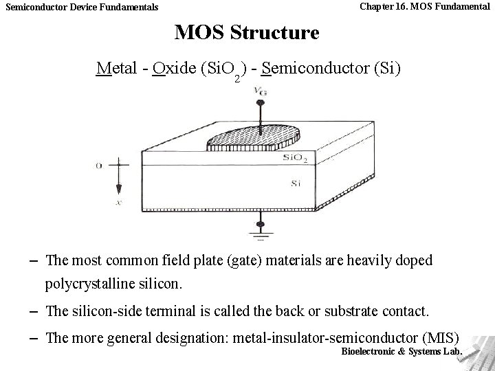
Chapter 16. MOS Fundamental Semiconductor Device Fundamentals MOS Structure Metal - Oxide (Si. O ) - Semiconductor (Si) 2 – The most common field plate (gate) materials are heavily doped polycrystalline silicon. – The silicon-side terminal is called the back or substrate contact. – The more general designation: metal-insulator-semiconductor (MIS) Bioelectronic & Systems Lab.

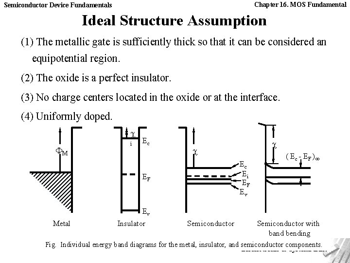
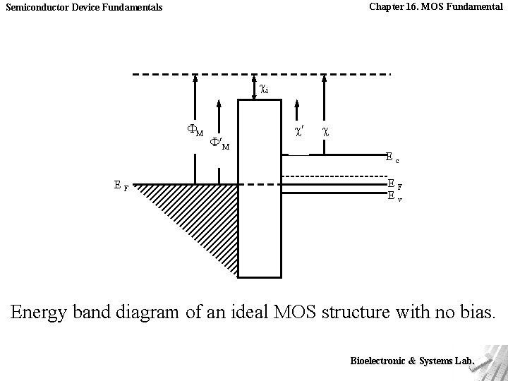
Chapter 16. MOS Fundamental Semiconductor Device Fundamentals Ideal Structure Assumption (1) The metallic gate is sufficiently thick so that it can be considered an equipotential region. (2) The oxide is a perfect insulator. (3) No charge centers located in the oxide or at the interface. (4) Uniformly doped. M i Ec Ei EF Ev EF ( E c - E F ) Ev Metal Insulator Semiconductor with band bending Fig. Individual energy band diagrams for the metal, insulator, and semiconductor components. Bioelectronic & Systems Lab.

Chapter 16. MOS Fundamental Semiconductor Device Fundamentals (5) The semiconductor is sufficiently thick so that a field-free region(“bulk”) is encountered before reaching the back contact. (6) An ohmic contact between the semiconductor and the metal on the back side. (7) One-dimensional structure. (8) No work function difference between metal and semiconductor. ( M = S) M i Ec Ei EF Ev EF ( E c - E F ) Ev Semiconductor with band bending Fig. Individual energy band diagrams for the metal, insulator, and semiconductor components. Metal Insulator Semiconductor Bioelectronic & Systems Lab.

Chapter 16. MOS Fundamental Semiconductor Device Fundamentals i M EF M Ec EF Ev Energy band diagram of an ideal MOS structure with no bias. Bioelectronic & Systems Lab.

Semiconductor Device Fundamentals Chapter 16. MOS Fundamental Effect Of An Applied Bias - Qualitative description • General observations – – Even with VG 0, semiconductor Fermi energy is unaffected by the bias and remains invariant as a function of position because of the assumed zero current flow. Bioelectronic & Systems Lab.

Semiconductor Device Fundamentals Chapter 16. MOS Fundamental – Since the barrier heights are fixed quantities, the movement of the metal Fermi level leads to a band bending. • In the metal, no band-bending. • In the oxide and semiconductor, an upward slope when VG>0 a downward slope when VG < 0. • With no oxide charges, the Poisson's equation yields a constant slope in the oxide. • Band bending in the semiconductor is somewhat more complex. Bioelectronic & Systems Lab.

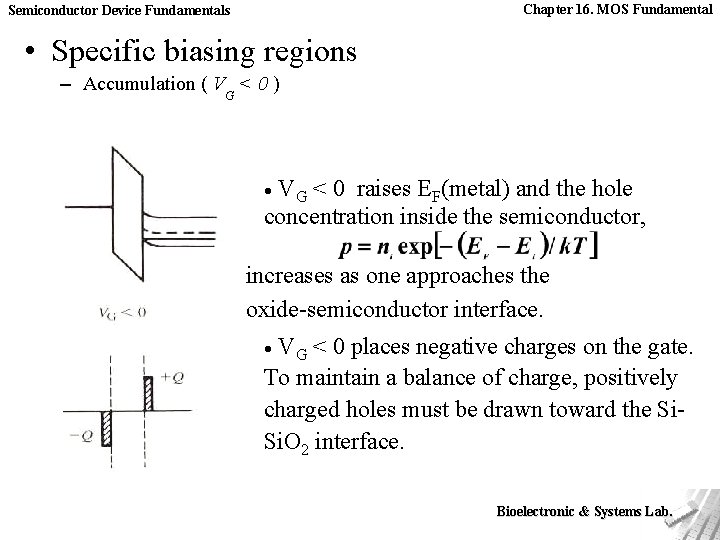
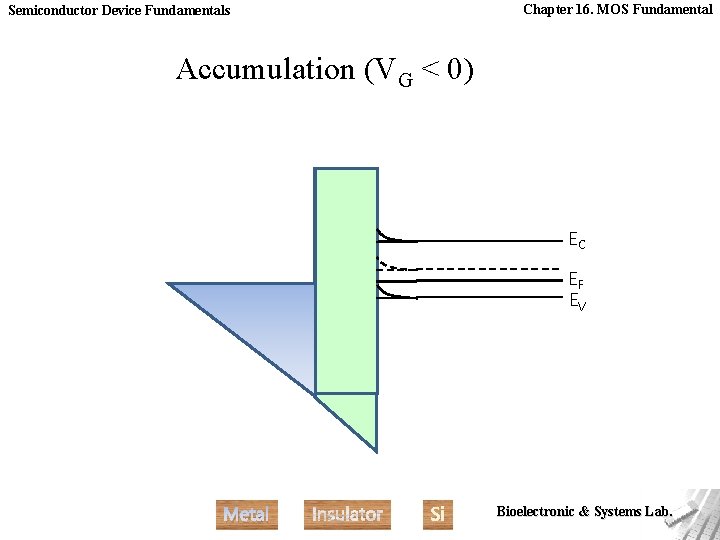
Chapter 16. MOS Fundamental Semiconductor Device Fundamentals • Specific biasing regions – Accumulation ( VG < 0 ) VG < 0 raises EF(metal) and the hole concentration inside the semiconductor, · increases as one approaches the oxide-semiconductor interface. VG < 0 places negative charges on the gate. To maintain a balance of charge, positively charged holes must be drawn toward the Si. O 2 interface. · Bioelectronic & Systems Lab.

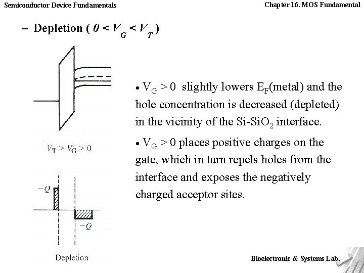
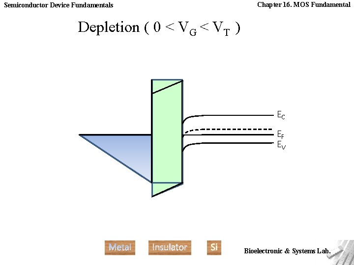
Chapter 16. MOS Fundamental Semiconductor Device Fundamentals – Depletion ( 0 < VG < VT ) VG > 0 slightly lowers EF(metal) and the hole concentration is decreased (depleted) in the vicinity of the Si-Si. O 2 interface. · VG > 0 places positive charges on the gate, which in turn repels holes from the interface and exposes the negatively charged acceptor sites. · Bioelectronic & Systems Lab.

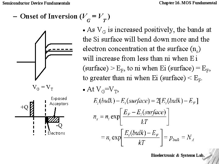
Chapter 16. MOS Fundamental Semiconductor Device Fundamentals – Onset of Inversion (VG = VT ) As VG is increased positively, the bands at the Si surface will bend down more and the electron concentration at the surface (ns) will increase from less than ni when E i (surface) > EF, to ni when Ei (surface) = EF, to greater than ni when Ei (surface) < EF. · VG = V T +Q · At VG=VT, Exposed Acceptors -Q Electrons Bioelectronic & Systems Lab.

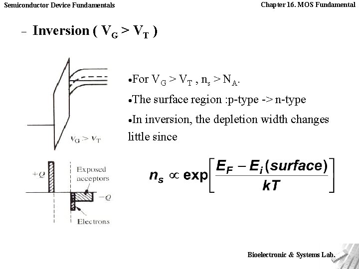
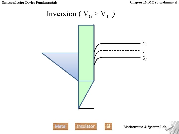
Chapter 16. MOS Fundamental Semiconductor Device Fundamentals - Inversion ( VG > VT ) ·For VG > VT , ns > NA. ·The surface region : p-type -> n-type ·In inversion, the depletion width changes little since Bioelectronic & Systems Lab.

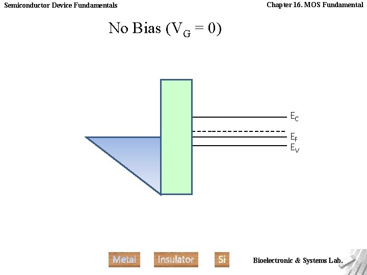
Semiconductor Device Fundamentals Chapter 16. MOS Fundamental No Bias (VG = 0) EC EF EV Metal Bioelectronic & Systems Lab.

Semiconductor Device Fundamentals Chapter 16. MOS Fundamental Accumulation (VG < 0) EC EF EV Metal Bioelectronic & Systems Lab.

Semiconductor Device Fundamentals Chapter 16. MOS Fundamental Depletion ( 0 < VG < VT ) EC EF EV Metal Bioelectronic & Systems Lab.

Semiconductor Device Fundamentals Chapter 16. MOS Fundamental Inversion ( VG > VT ) EC EF EV Metal Bioelectronic & Systems Lab.

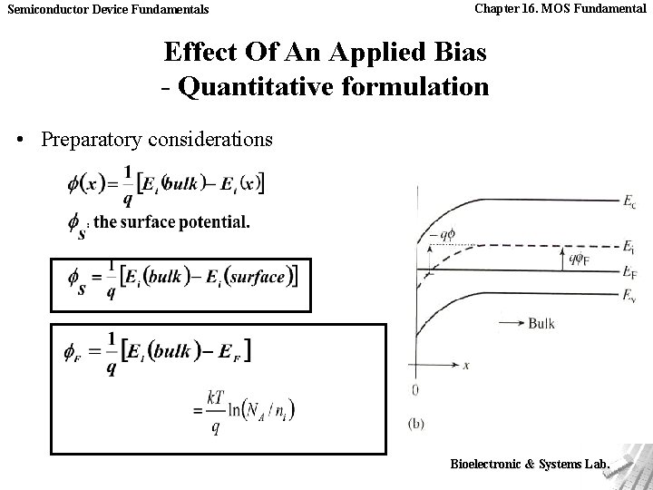
Semiconductor Device Fundamentals Chapter 16. MOS Fundamental Effect Of An Applied Bias - Quantitative formulation • Preparatory considerations Bioelectronic & Systems Lab.

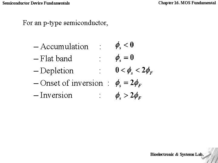
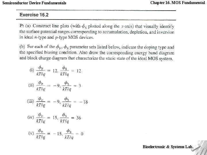
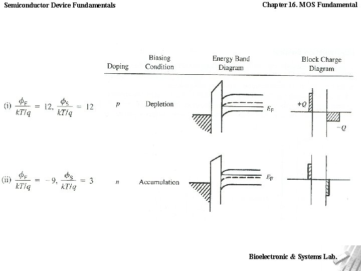
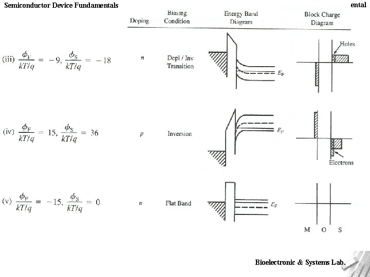
Semiconductor Device Fundamentals Chapter 16. MOS Fundamental For an p-type semiconductor, – Accumulation : – Flat band : – Depletion : – Onset of inversion : – Inversion : Bioelectronic & Systems Lab.

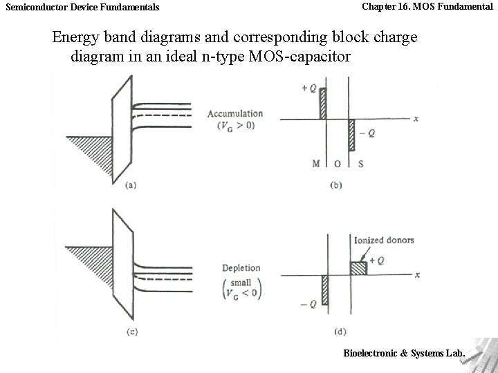
Semiconductor Device Fundamentals Chapter 16. MOS Fundamental Energy band diagrams and corresponding block charge diagram in an ideal n-type MOS-capacitor Bioelectronic & Systems Lab.

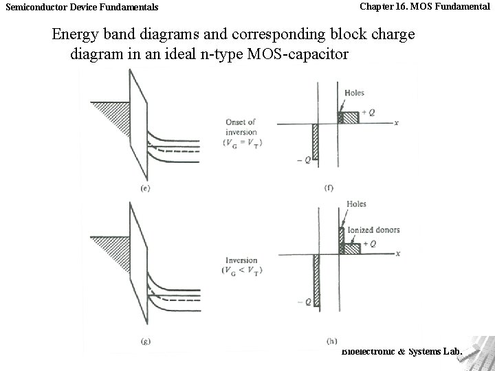
Semiconductor Device Fundamentals Chapter 16. MOS Fundamental Energy band diagrams and corresponding block charge diagram in an ideal n-type MOS-capacitor Bioelectronic & Systems Lab.

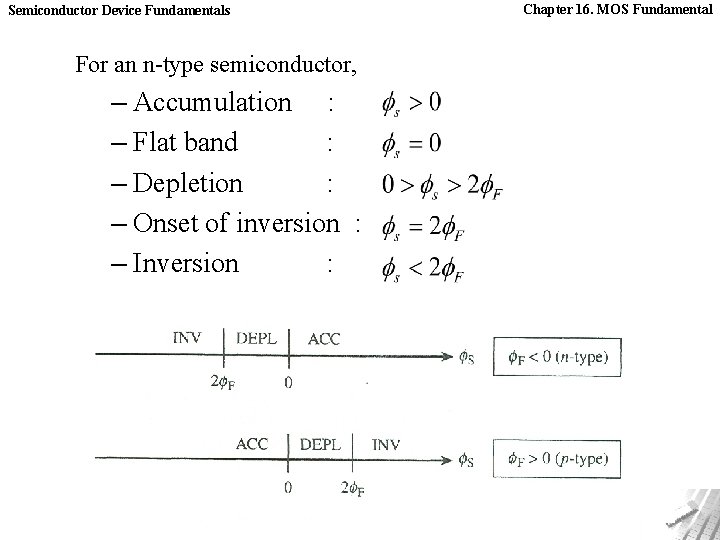
Semiconductor Device Fundamentals Chapter 16. MOS Fundamental For an n-type semiconductor, – Accumulation : – Flat band : – Depletion : – Onset of inversion : – Inversion : Bioelectronic & Systems Lab.

Semiconductor Device Fundamentals Chapter 16. MOS Fundamental Bioelectronic & Systems Lab.

Semiconductor Device Fundamentals Chapter 16. MOS Fundamental Bioelectronic & Systems Lab.

Semiconductor Device Fundamentals Chapter 16. MOS Fundamental Bioelectronic & Systems Lab.

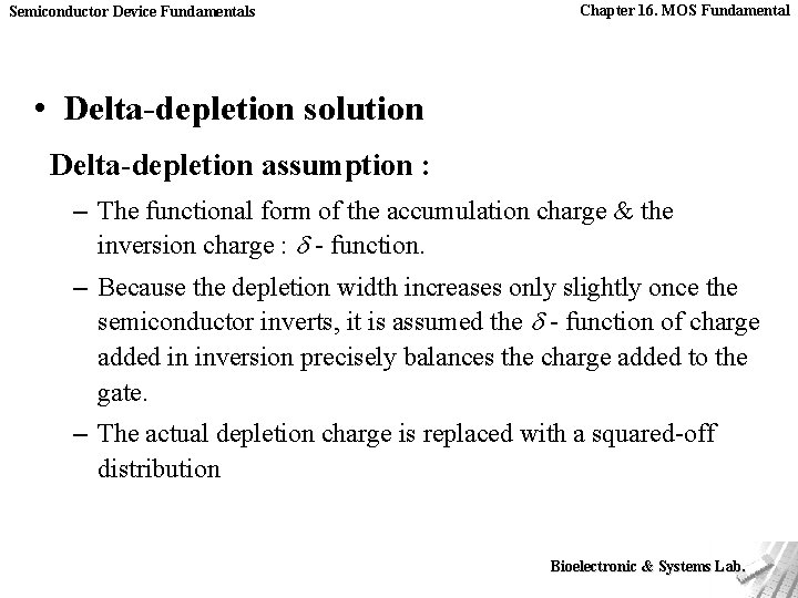
Semiconductor Device Fundamentals Chapter 16. MOS Fundamental • Delta-depletion solution Delta-depletion assumption : – The functional form of the accumulation charge & the inversion charge : - function. – Because the depletion width increases only slightly once the semiconductor inverts, it is assumed the - function of charge added in inversion precisely balances the charge added to the gate. – The actual depletion charge is replaced with a squared-off distribution Bioelectronic & Systems Lab.

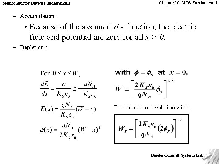
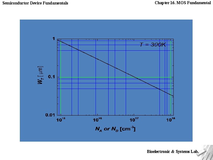
Semiconductor Device Fundamentals Chapter 16. MOS Fundamental – Accumulation : • Because of the assumed - function, the electric field and potential are zero for all x > 0. – Depletion : The maximum depletion width, Bioelectronic & Systems Lab.

Semiconductor Device Fundamentals Chapter 16. MOS Fundamental Bioelectronic & Systems Lab.

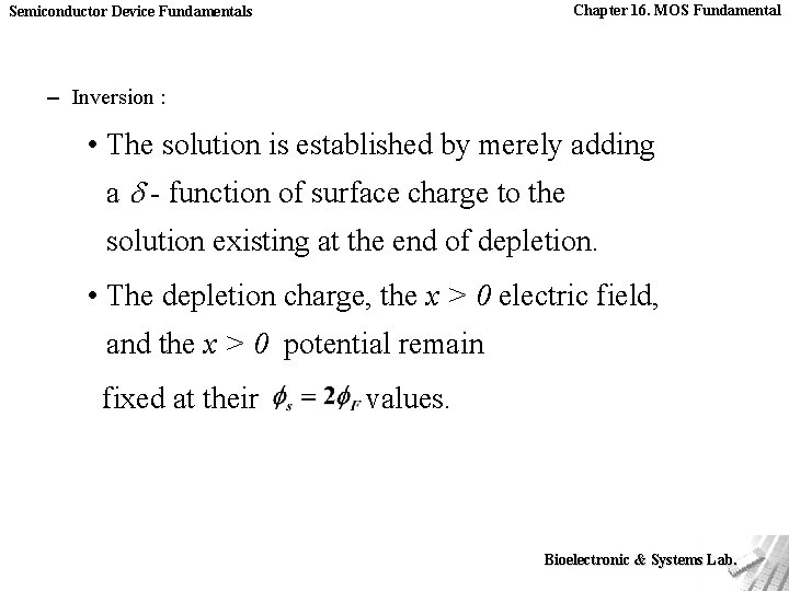
Chapter 16. MOS Fundamental Semiconductor Device Fundamentals – Inversion : • The solution is established by merely adding a - function of surface charge to the solution existing at the end of depletion. • The depletion charge, the x > 0 electric field, and the x > 0 potential remain fixed at their values. Bioelectronic & Systems Lab.

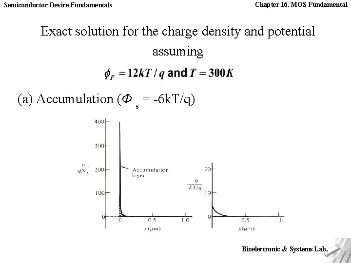
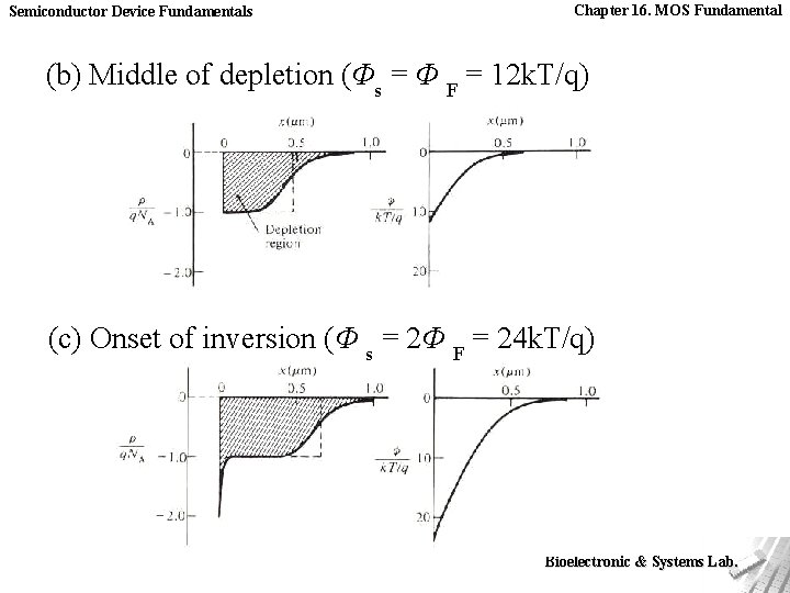
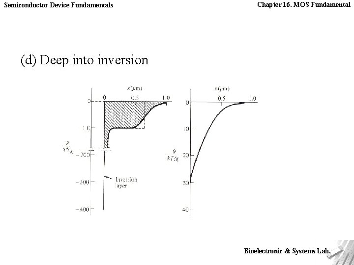
Semiconductor Device Fundamentals Chapter 16. MOS Fundamental Exact solution for the charge density and potential assuming (a) Accumulation (Φ s = -6 k. T/q) Bioelectronic & Systems Lab.

Semiconductor Device Fundamentals Chapter 16. MOS Fundamental (b) Middle of depletion (Φs = Φ F = 12 k. T/q) (c) Onset of inversion (Φ s = 2Φ F = 24 k. T/q) Bioelectronic & Systems Lab.

Semiconductor Device Fundamentals Chapter 16. MOS Fundamental (d) Deep into inversion Bioelectronic & Systems Lab.

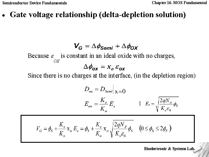
Semiconductor Device Fundamentals · Chapter 16. MOS Fundamental Gate voltage relationship (delta-depletion solution) Because OX is constant in an ideal oxide with no charges, Since there is no charges at the interface, (in the depletion region) Bioelectronic & Systems Lab.

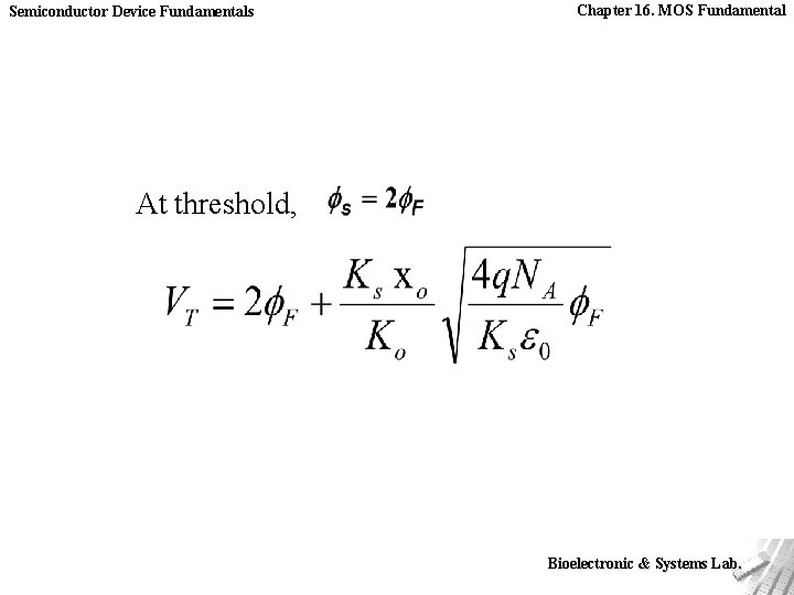
Semiconductor Device Fundamentals Chapter 16. MOS Fundamental At threshold, Bioelectronic & Systems Lab.

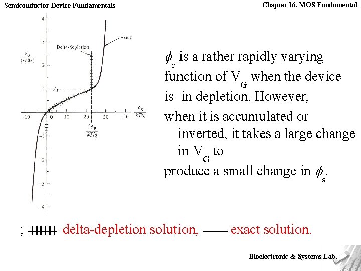
Chapter 16. MOS Fundamental Semiconductor Device Fundamentals fs is a rather rapidly varying function of VG when the device is in depletion. However, when it is accumulated or inverted, it takes a large change in VG to produce a small change in fs. ; delta-depletion solution, exact solution. Bioelectronic & Systems Lab.

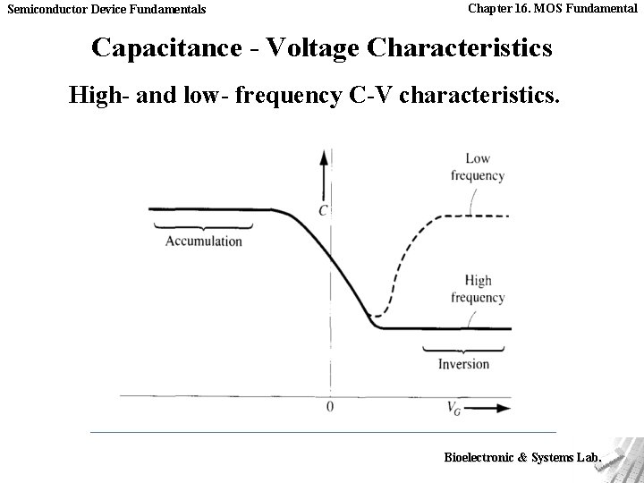
Semiconductor Device Fundamentals Chapter 16. MOS Fundamental Capacitance - Voltage Characteristics High- and low- frequency C-V characteristics. Bioelectronic & Systems Lab.

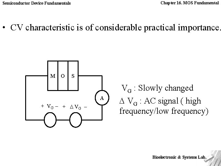
Chapter 16. MOS Fundamental Semiconductor Device Fundamentals • CV characteristic is of considerable practical importance. M O S A + V G – + VG – VG : Slowly changed VG : AC signal ( high frequency/low frequency) Bioelectronic & Systems Lab.

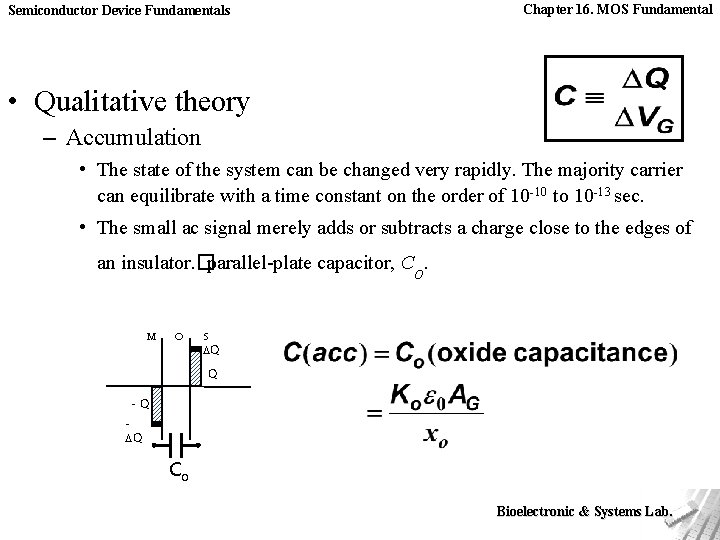
Semiconductor Device Fundamentals Chapter 16. MOS Fundamental • Qualitative theory – Accumulation • The state of the system can be changed very rapidly. The majority carrier can equilibrate with a time constant on the order of 10 -10 to 10 -13 sec. • The small ac signal merely adds or subtracts a charge close to the edges of an insulator. �parallel-plate capacitor, CO. M O S Q Q -Q Q Co Bioelectronic & Systems Lab.

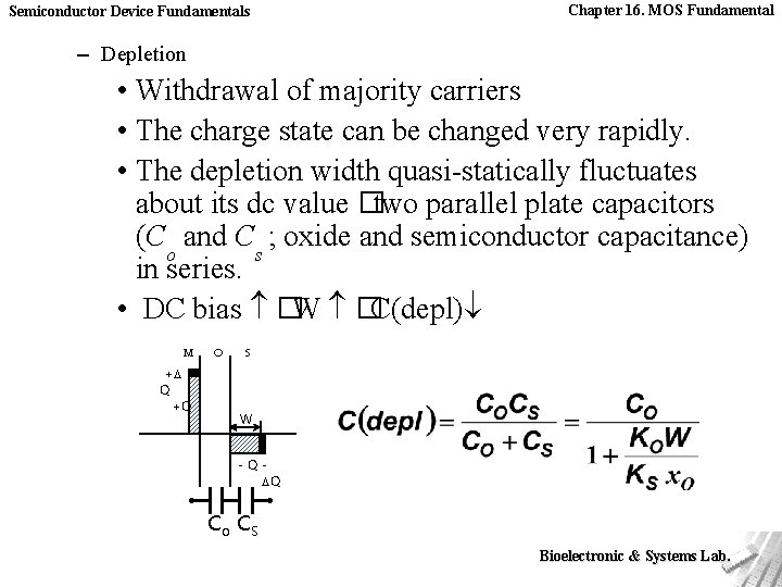
Semiconductor Device Fundamentals Chapter 16. MOS Fundamental – Depletion • Withdrawal of majority carriers • The charge state can be changed very rapidly. • The depletion width quasi-statically fluctuates about its dc value �two parallel plate capacitors (Co and Cs ; oxide and semiconductor capacitance) in series. • DC bias �W �C(depl) M + Q +Q O S W -Q Q Co CS Bioelectronic & Systems Lab.

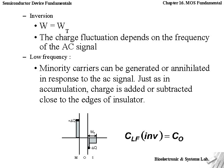
Chapter 16. MOS Fundamental Semiconductor Device Fundamentals – Inversion • W = WT • The charge fluctuation depends on the frequency of the AC signal – Low frequency : • Minority carriers can be generated or annihilated in response to the ac signal. Just as in accumulation, charge is added or subtracted close to the edges of insulator. + Q WT - Q M O S Bioelectronic & Systems Lab.

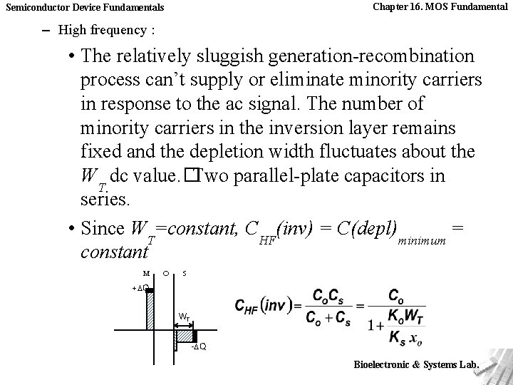
Chapter 16. MOS Fundamental Semiconductor Device Fundamentals – High frequency : • The relatively sluggish generation-recombination process can’t supply or eliminate minority carriers in response to the ac signal. The number of minority carriers in the inversion layer remains fixed and the depletion width fluctuates about the WT dc value. �Two parallel-plate capacitors in series. • Since WT=constant, CHF(inv) = C(depl)minimum = constant M O S + Q WT - Q Bioelectronic & Systems Lab.

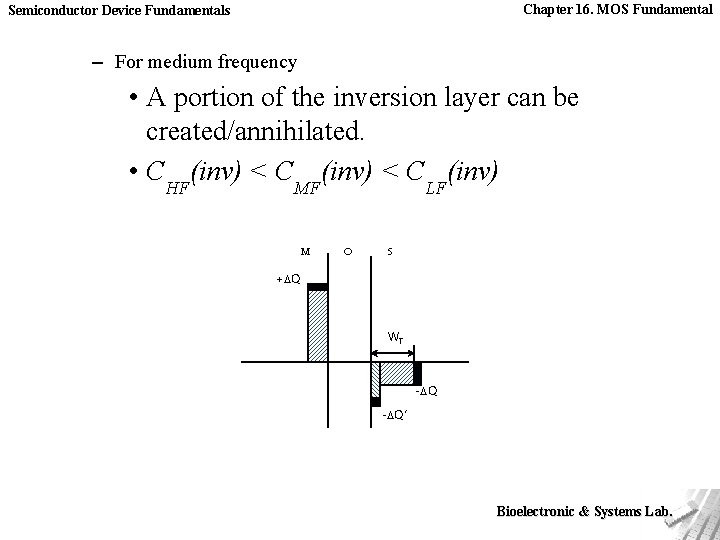
Chapter 16. MOS Fundamental Semiconductor Device Fundamentals – For medium frequency • A portion of the inversion layer can be created/annihilated. • CHF(inv) < CMF(inv) < CLF(inv) M O S + Q WT - Q’ Bioelectronic & Systems Lab.

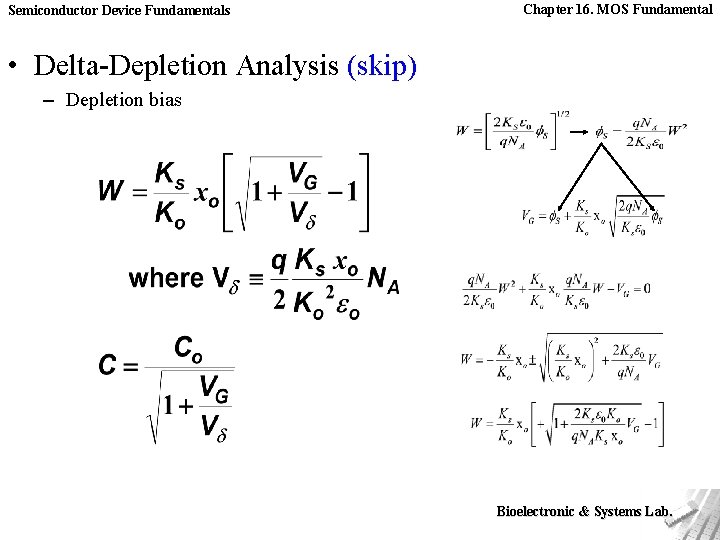
Semiconductor Device Fundamentals Chapter 16. MOS Fundamental • Delta-Depletion Analysis (skip) – Depletion bias Bioelectronic & Systems Lab.

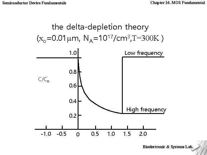
Chapter 16. MOS Fundamental Semiconductor Device Fundamentals the delta-depletion theory (xo=0. 01 mm, NA=1017/cm 3, T=300 K ) 1. 0 Low frequency 0. 8 C/Co 0. 6 0. 4 High frequency 0. 2 -1. 0 -0. 5 0 0. 5 1. 0 1. 5 2. 0 Bioelectronic & Systems Lab.

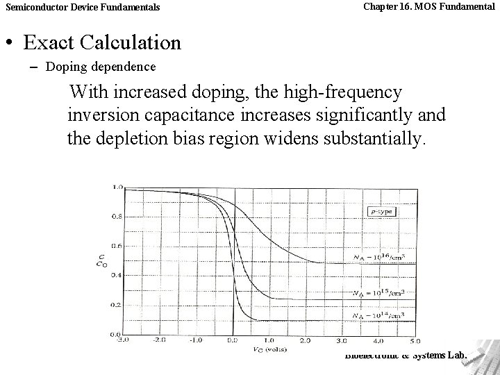
Semiconductor Device Fundamentals Chapter 16. MOS Fundamental • Exact Calculation – Doping dependence With increased doping, the high-frequency inversion capacitance increases significantly and the depletion bias region widens substantially. Bioelectronic & Systems Lab.

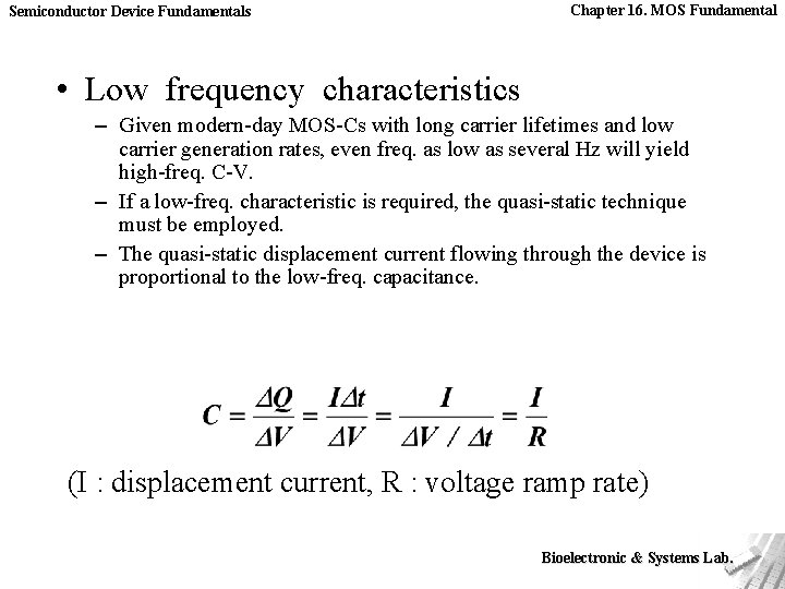
Semiconductor Device Fundamentals Chapter 16. MOS Fundamental • Low frequency characteristics – Given modern-day MOS-Cs with long carrier lifetimes and low carrier generation rates, even freq. as low as several Hz will yield high-freq. C-V. – If a low-freq. characteristic is required, the quasi-static technique must be employed. – The quasi-static displacement current flowing through the device is proportional to the low-freq. capacitance. (I : displacement current, R : voltage ramp rate) Bioelectronic & Systems Lab.

Semiconductor Device Fundamentals Chapter 16. MOS Fundamental • High frequency characteristics – Normal measurement frequency ~ 1 MHz. – In the ramped-measurement, a deep-depletion phenomenon may appear. Bioelectronic & Systems Lab.

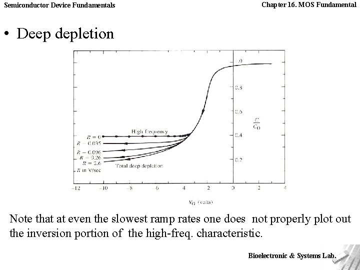
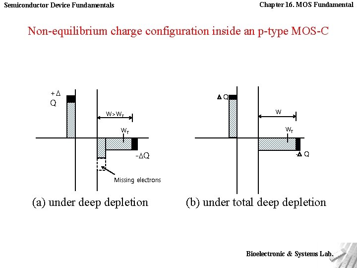
Semiconductor Device Fundamentals Chapter 16. MOS Fundamental • Deep depletion Note that at even the slowest ramp rates one does not properly plot out the inversion portion of the high-freq. characteristic. Bioelectronic & Systems Lab.

Semiconductor Device Fundamentals Chapter 16. MOS Fundamental – In accumulation or depletion, only majority carriers are involved � Charge configuration rapidly reacts to the changing gate bias. – In inversion region, minority carriers should be generated – The generation process is sluggish and has difficulty supplying the minority carriers needed for the structure to equilibrate. Bioelectronic & Systems Lab.

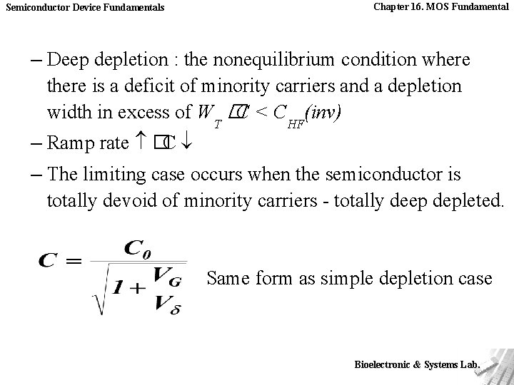
Semiconductor Device Fundamentals Chapter 16. MOS Fundamental – Deep depletion : the nonequilibrium condition where there is a deficit of minority carriers and a depletion width in excess of WT �C < CHF(inv) – Ramp rate �C – The limiting case occurs when the semiconductor is totally devoid of minority carriers - totally deep depleted. Same form as simple depletion case Bioelectronic & Systems Lab.

Chapter 16. MOS Fundamental Semiconductor Device Fundamentals Non-equilibrium charge configuration inside an p-type MOS-C + Q Q W W>WT WT WT - Q Missing electrons (a) under deep depletion (b) under total deep depletion Bioelectronic & Systems Lab.