SRAM Memory External Interface A 0 A 9


 E")


 RAS’ Column Row Data BURST From Prof. Sankaralingam, UWisc-Madison")


- Slides: 58
SRAM Memory External Interface A 0 -A 9 D 0 R/W! E 1 Kbit SRAM GEOMETRY: ( ROWS , COLS ) == ADDRESSES x DATA WIDTH CAPACITY
Making Wider Memories • WANT A 0 -A 9 HAVE D 0 -D 1 A 0 -A 9 R/W! E E 1 Kx 2 bit SRAM D 0 1 Kx 1 bit SRAM
Making Wider Memories A 0 -A 10 A 0 -A 9 D 0 R/W! E R/W! A 0 -A 9 R/W! E E 2 Kx 1 bit SRAM D 0 D 1 D 0 -D 1
Making Taller Memories • WANT A 0 -A 10 HAVE D 0 A 0 -A 9 R/W! E E 2 Kx 1 bit SRAM D 0 1 Kx 1 bit SRAM
Making Taller Memories • WANT A 0 -A 10 HAVE D 0 A 0 -A 9 R/W! E E 2 Kx 1 bit SRAM D 0 1 Kx 1 bit SRAM
Making Taller Memories A 0 -A 10 D 0 A 0 -A 9 R/W! E E 2 Kx 1 bit SRAM D 0 1 Kx 1 bit SRAM
Address Mapping 0 00000 1 K rows 0 11111 1 00000 1 11111 2 K rows
Address Mapping 0 XXXXX 1 K rows 2 K rows A 10 1 XXXXX
Making Taller Memories A 0 -A 9 A 0 -A 10 A 0 -A 9 D 0 R/W! A 10 E R/W! A 0 -A 9 R/W! E E 2 Kx 1 bit SRAM D 0 D 0
Making Taller Memories A 0 -A 11 D 0 A 0 -A 9 R/W! E E 4 Kx 1 bit SRAM D 0 1 Kx 1 bit SRAM
Address Mapping 00 00000 1 K rows 00 11111 01 00000 01 11111 10 00000 10 11111 11 00000 11 11111 4 K rows
Address Mapping 00 XXXXX 1 K rows 01 XXXXX 4 K rows 10 XXXXX 11 XXXXX
Making Taller Memories A 0 -A 11 A 0 -A 9 D 0 R/W! A 11 -A 10 E R/W! A 0 -A 9 D 0 R/W! E E A 0 -A 9 D 0 R/W! E A 0 -A 9 R/W! E D 0 D 0
Where is the decoder? A 0 -A 9 A 0 -A 10 A 0 -A 9 D 0 R/W! A 10 E R/W! A 0 -A 9 R/W! E E 2 Kx 1 bit SRAM D 0 D 0
Memory External Interface A 0 -A 9 D 0 R/W! E 1 Kbit SRAM
SRAM Internal Organization A 0 -A 9 SRAM bit Wire delay = f(length^2) E Decoder R/W! Sense Amp D 0
SRAM Internal Organization A 0 -A 4 A 0 -A 9 s Row Decoder u 32 x 32 array q s s A R/W! A 5 -A 9 Column Mux D 0 E e ar a o p s le sib
Wider Data Bus A 0 -A 4 A 0 -A 9 Row Decoder R/W! A 5 -A 9 E 32 x 32 array Column Mux D 3 D 2 D 1 D 0
Wider Data Bus A 0 -A 4 A 0 -A 9 s Row Decoder u 32 x 32 array q s s A R/W! A 5 -A 9 Column Mux D 0 -D 3 E D 0 -D 3 e ar a o p s le sib
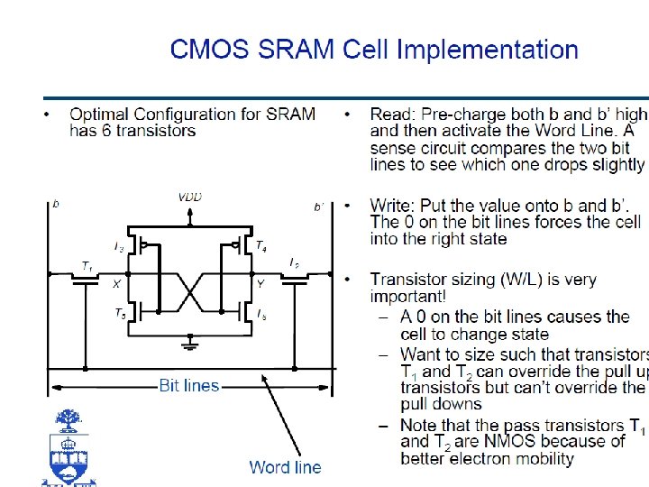
SRAM Bit Cell 6 T Cell bitline! bitline row select bit-cell array 2 n n -Read Sequence 1. precharge all bitlines 2. address decode 3. drive row select 4. selected bit-cells drive bitlines 5. diff. sensing and col. select n+m 2 n row x 2 m-col (n m to minmize overall latency) m 2 m diff pairs sense amp and mux 1 From Prof. Sankaralingam, UWisc-Madison
SRAM Bit Cell - Precharge Vdd bitline! bitline wordline
SRAM Bit Cell – Decode Row and Select bitline! bitline row select
SRAM Bit Cell – Mux and Sense bitline! bitline row select
SRAM Bit Cell – Mux and Sense bitline! bitline row select
SRAM Bit Cell – Writes 0 1 bitline! bitline row select
Memory Array From prof. Gulak’s Slides
Decoders users. ece. utexas. edu/~adnan/vlsi-05 -backup/lec 13 SRAM. ppt
Larger Decoders • For N>4 NAND becomes slow • Use 2 -input gates hierarchically users. ece. utexas. edu/~adnan/vlsi-05 -backup/lec 13 SRAM. ppt
Pre-Decoding • Many gates are redundant – Saves area
Dynamic RAM • _bitline wordline • • RAS bit-cell array 2 n n 2 n row x 2 m-col (n m to minmize overall latency) m CAS 2 m sense amp and mux 1 • Value is stored on a capacitor C – single pass transistor T connects C to the bit line when the cell is being read or written C experiences leakage meaning the charge stored on C will slowly leak out, thus destroying the value To prevent this DRAM cells need to be periodically refreshed – emory controller goes through and reads all the cells and then writes the same values back DRAM cells have a different manufacturing process than processors so it’s difficult and expensive to incorporate them onto the same chip A DRAM die comprises of multiple such arrays From Prof. Sankaralingam, UWisc-Madison
_bitline wordline From http: //en. wikipedia. org/wiki/File: DRAM_trench_structure_configuration 1_1. svg
DRAM Notes • Read: – Bit line is pre-charged and then word line is activated. If there is a 1 in the capacitor, then the bit line remains high. Otherwise it gets pulled down • Write: – Bit line is driven to the write value and either charges or drains the capacitor writing the value into it. • Refresh adds overhead: – Usually each cell has to be refreshed every 64 ms – Cell is unavailable for 2 -4% of refresh period (i. e. 1. 2 to 2. 4 ms of each 64 ms period) – Memory controller tries to schedule refreshes so they don’t interfere with regular memory traffic – Self-Refreshing memories
Synchronous DRAM http: //search. library. utoronto. ca/details? 6949501 Memory Systems Cache, DRAM, Disk About this Book Author(s): Bruce Jacob, Spencer W. Ng, David T. Wang and Samuel Rodriguez
Synchronous DRAM (SDRAM) RAS’ Column Row Data BURST From Prof. Sankaralingam, UWisc-Madison
DDR 2 (Double Data Rate RAS’ Column Row Data From Prof. Sankaralingam, UWisc-Madison
Addressing in Modern DRAM
DRAM Organization Alternatives • 128 MB DRAM Capacity • 64 -bit data bus – 1 Gbit capacity • 64 MBit w/ 4 -bit data bus? • 64 Mbit w/ 8 -bit data bus? • 128 Mbit w/ 16 -bit data bus?
DRAM Organization Alternatives • 128 MB DRAM Capacity • 64 -bit data bus – 1 Gbit capacity • 64 MBit w/ 4 -bit data bus? – 64 bit bus? 16 devices – 16 x 64 Mb = 1 Gbit • 64 Mbit w/ 8 -bit data bus? – 64 -bit bus? 8 devices – Capacity? 8 x 64 Mbit = 512 Mbit 2 ranks • 128 Mbit w/ 16 -bit data bus? – 64 -bit bus? 4 devices – 1 Gbit capacity
• Home > Computer Hardware > Memory > Desktop Memory > Mushkin Enhanced > Item#: N 82 E 16820146744 • • • Mushkin Enhanced Essentials 2 GB 240 -Pin DDR 3 SDRAM DDR 3 1333 (PC 3 10666) Desktop Memory Model 991586 • DDR 3 1333 (PC 3 10666) • Timing 9 -9 -9 -24 • Cas Latency 9 • Voltage 1. 5 V
DDR 3 1333 • Operates at 667 Mhz • Can tranfer data at double the rate – Bandwidth 1333 MT/sec • Mega transfers per second
DRAM Access Sequence • • • 1. Precharge 2. Row Access 3. Column Access 4. Data Transfer 5. Close Row (write data back)
DRAM Timing • t. CAS-t. RCD-t. RP-t. RAS • t. CAS: column address strobe column to data appearing • t. RCD: – RAS to CAS row to column • t. RP: – RAS precharge, Precharge latency • t. RAS: – Row Access Strobe: Shortest time between two Row activations
DDR 3 Timing • Timing 9 -9 -9 -24 • t. CAS-t. RCD-t. RP-t. RAS
DDR DRAM Timing 9 -9 -9 -24 t. CAS-t. RCD-t. RP-t. RAS From anandtech: http: //images. anandtech. com/doci/3851/Back%20 to%20 Back%20 Burst%20 Read%20 with%20 Page%20 Close. png
Interleaved Main Memory • Divide memory into M banks and “interleave” addresses across them, so word A is – in bank (A mod M) – at word (A div M) Bank 0 Bank 1 word 0 word n word 2 n word 1 word n+1 word 2 n+1 Bank 2 Bank n word 2 word n+2 word 2 n+2 word n-1 word 2 n-1 word 3 n-1 PA Doubleword in bank Bank Word in doubleword Interleaved memory increases memory BW without wider bus • Use parallelism in memory banks to hide memory latency Copyright © 2002 Falsafi, from Hill, Smith, Sohi, Vijaykumar, and Wood 47
Flash Memory gate Floating gate n n p
Flash Memory “ 1” “ 0” - ------ - --- n n p n Trapped charge n p • Floating gate changes threshold voltage • SLC 2 states • MLC more states
Flash Memory -- Reading gate Voltage Floating gate n n p
Flash Memory – Writing a “ 0” gate High Possitive Voltage ------ ---n n p
Flash Memory – Writing a “ 1” gate High negative Voltage n n p
NAND FLASH
NAND FLASH Reading Conduct no matter what value Conduct only if no charge Von Von VA Von Von Von
NAND FLASH Erasing Clear off all charge: negative Von Ve Ve Von
NAND FLASH Writing Conduct no matter what value High possitive Von Von VA Von Von Von