Plan for Memory Technologies Topic Static RAM SRAM
- Slides: 16

Plan for Memory Technologies Topic • • Static RAM (SRAM) Dynamic RAM (DRAM) Memory Hierarchy DRAM Accelerating Techniques – Reading B. 5 COMP 203/NWEN 201 2009 Memory Technologies 0

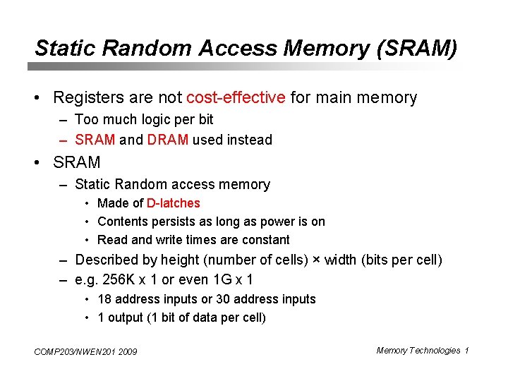
Static Random Access Memory (SRAM) • Registers are not cost-effective for main memory – Too much logic per bit – SRAM and DRAM used instead • SRAM – Static Random access memory • Made of D-latches • Contents persists as long as power is on • Read and write times are constant – Described by height (number of cells) × width (bits per cell) – e. g. 256 K x 1 or even 1 G x 1 • 18 address inputs or 30 address inputs • 1 output (1 bit of data per cell) COMP 203/NWEN 201 2009 Memory Technologies 1

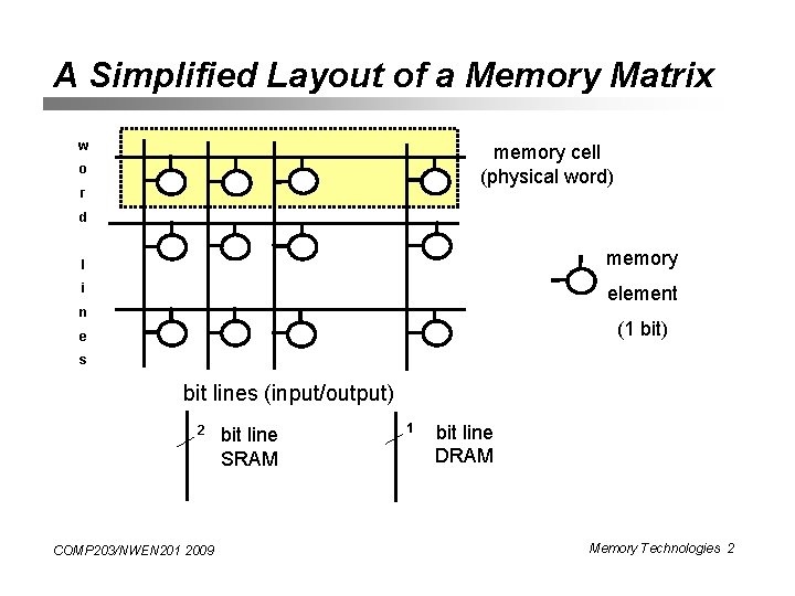
A Simplified Layout of a Memory Matrix w memory cell (physical word) o r d memory l i element n (1 bit) e s bit lines (input/output) 2 COMP 203/NWEN 201 2009 bit line SRAM 1 bit line DRAM Memory Technologies 2

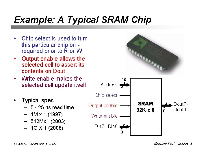
Example: A Typical SRAM Chip • Chip select is used to turn this particular chip on required prior to R or W • Output enable allows the selected cell to assert its contents on Dout • Write enable makes the selected cell update itself • Typical spec – – 5 - 25 ns read time 4 M x 1 (1997) 512 Mx 1 (2003) 1 G X 1 (2008) COMP 203/NWEN 201 2009 15 Address Chip select SRAM 32 K x 8 Output enable 8 Dout 7 Dout 0 Write enable Din 7 - Din 0 8 Memory Technologies 3

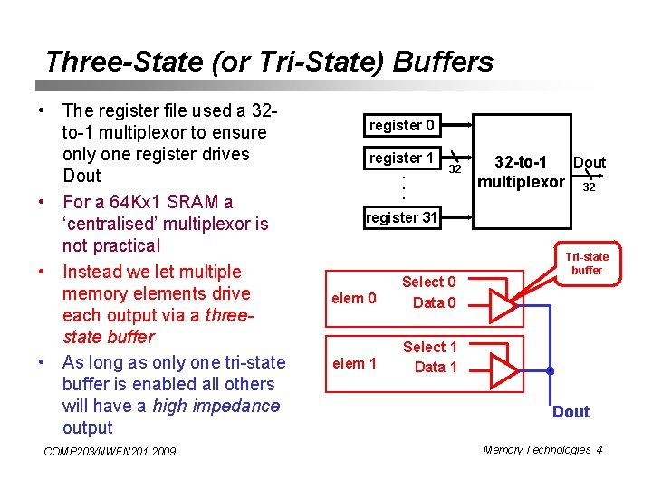
Three-State (or Tri-State) Buffers • The register file used a 32 to-1 multiplexor to ensure only one register drives Dout • For a 64 Kx 1 SRAM a ‘centralised’ multiplexor is not practical • Instead we let multiple memory elements drive each output via a threestate buffer • As long as only one tri-state buffer is enabled all others will have a high impedance output COMP 203/NWEN 201 2009 register 0 register 1. . . 32 Dout 32 -to-1 multiplexor 32 register 31 elem 0 Select 0 Data 0 elem 1 Select 1 Data 1 Tri-state buffer Dout Memory Technologies 4

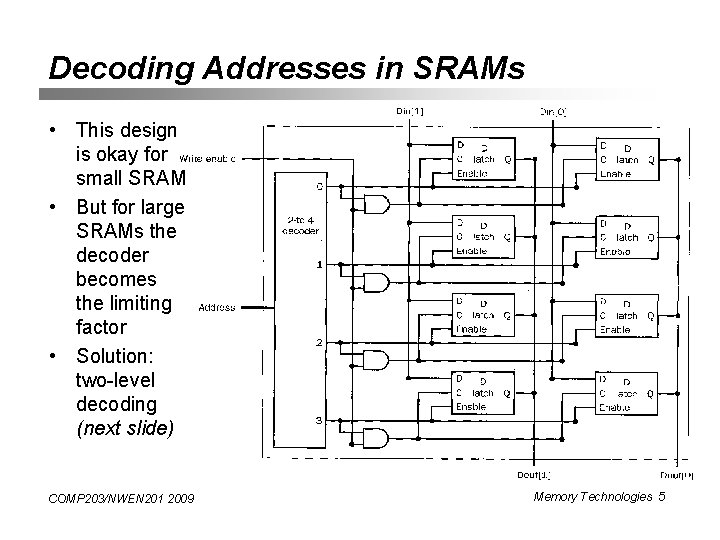
Decoding Addresses in SRAMs • This design is okay for small SRAM • But for large SRAMs the decoder becomes the limiting factor • Solution: two-level decoding (next slide) COMP 203/NWEN 201 2009 Memory Technologies 5

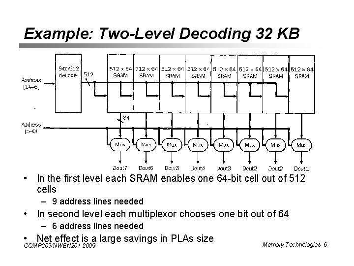
Example: Two-Level Decoding 32 KB • In the first level each SRAM enables one 64 -bit cell out of 512 cells – 9 address lines needed • In second level each multiplexor chooses one bit out of 64 – 6 address lines needed • Net effect is a large savings in PLAs size COMP 203/NWEN 201 2009 Memory Technologies 6

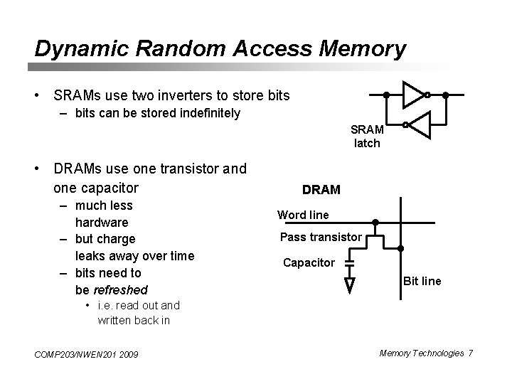
Dynamic Random Access Memory • SRAMs use two inverters to store bits – bits can be stored indefinitely SRAM latch • DRAMs use one transistor and one capacitor – much less hardware – but charge leaks away over time – bits need to be refreshed DRAM Word line Pass transistor Capacitor Bit line • i. e. read out and written back in COMP 203/NWEN 201 2009 Memory Technologies 7

Refreshing Mechanisms • Can be done by processor – but to refresh megabytes several times a second becomes costly • More often done by memory chips themselves – entire rows can be refreshed at once – approximately 1% of memory cycles are lost to refreshing COMP 203/NWEN 201 2009 Memory Technologies 8

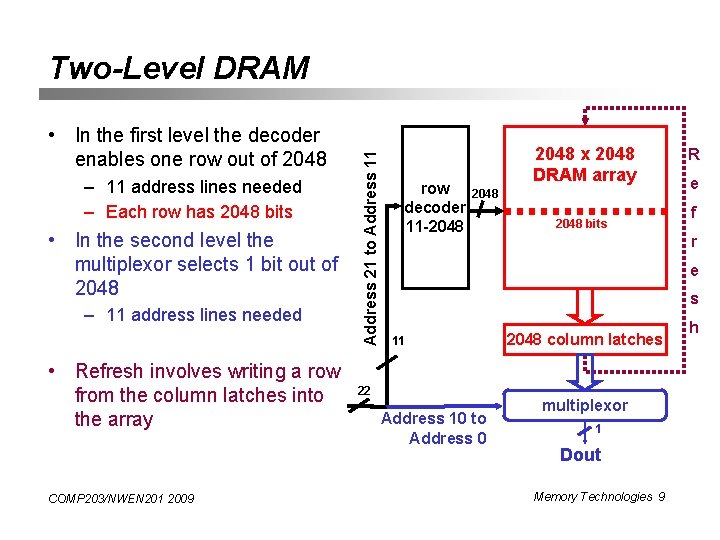
• In the first level the decoder enables one row out of 2048 – 11 address lines needed – Each row has 2048 bits • In the second level the multiplexor selects 1 bit out of 2048 – 11 address lines needed • Refresh involves writing a row from the column latches into the array COMP 203/NWEN 201 2009 Address 21 to Address 11 Two-Level DRAM row decoder 11 -2048 x 2048 DRAM array 2048 bits R e f r e s 11 22 Address 10 to Address 0 2048 column latches multiplexor 1 Dout Memory Technologies 9 h

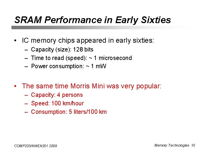
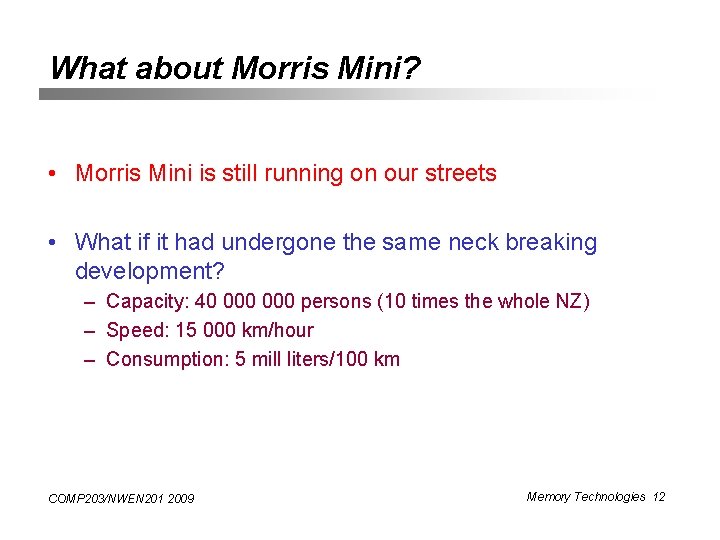
SRAM Performance in Early Sixties • IC memory chips appeared in early sixties: – Capacity (size): 128 bits – Time to read (speed): ~ 1 microsecond – Power consumption: ~ 1 m. W • The same time Morris Mini was very popular: – Capacity: 4 persons – Speed: 100 km/hour – Consumption: 5 liters/100 km COMP 203/NWEN 201 2009 Memory Technologies 10

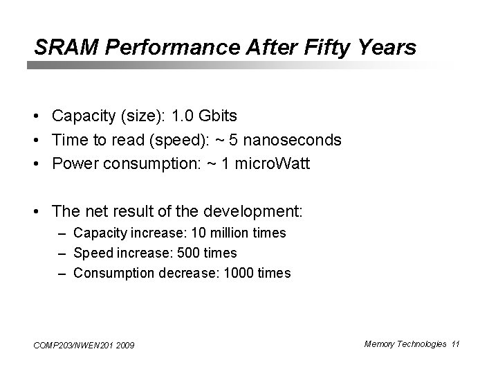
SRAM Performance After Fifty Years • Capacity (size): 1. 0 Gbits • Time to read (speed): ~ 5 nanoseconds • Power consumption: ~ 1 micro. Watt • The net result of the development: – Capacity increase: 10 million times – Speed increase: 500 times – Consumption decrease: 1000 times COMP 203/NWEN 201 2009 Memory Technologies 11

What about Morris Mini? • Morris Mini is still running on our streets • What if it had undergone the same neck breaking development? – Capacity: 40 000 persons (10 times the whole NZ) – Speed: 15 000 km/hour – Consumption: 5 mill liters/100 km COMP 203/NWEN 201 2009 Memory Technologies 12

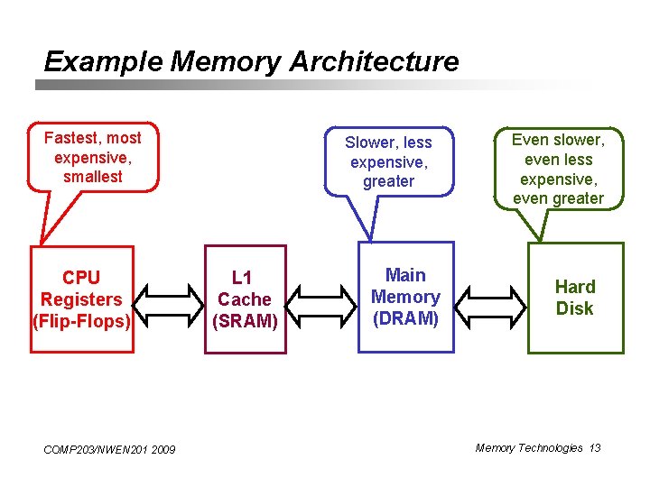
Example Memory Architecture Fastest, most expensive, smallest CPU Registers (Flip-Flops) COMP 203/NWEN 201 2009 Slower, less expensive, greater L 1 Cache (SRAM) Main Memory (DRAM) Even slower, even less expensive, even greater Hard Disk Memory Technologies 13

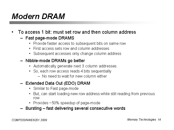
Modern DRAM • To access 1 bit: must set row and then column address – Fast page-mode DRAMS • Provide faster access to subsequent bits on same row • First access sets row and column addresses • Subsequent accesses only change column address – Nibble-mode DRAMs go better • Automatically generate next 3 column addresses • So, each row access reads 4 bits sequentially – No need to wait for new column either – Extended Data Out (EDO) DRAM • Similar to Fast page-mode • But, can start loading new row address while still reading from previous row • Provides ~50% speedup of page-mode – Bursting – fast delivering several consecutive words COMP 203/NWEN 201 2009 Memory Technologies 14

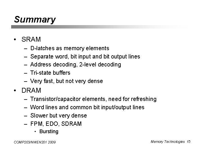
Summary • SRAM – – – D-latches as memory elements Separate word, bit input and bit output lines Address decoding, 2 -level decoding Tri-state buffers Very fast, but not very dense • DRAM – – Transistor/capacitor elements, need for refreshing Word lines and common bit input/output lines Slower but very dense FPM, EDO, SDRAM • Bursting COMP 203/NWEN 201 2009 Memory Technologies 15