1 JTAG INTERFACE SRAM TESTER WITH CLCM Reporter


![Working distribution 3 SRAM [johnny 751125] hcsoso、jackson 59、Sinze Tester [kcir] Coding mimi 9126、troychang、JAST、 gomibako、reeetingay](https://slidetodoc.com/presentation_image_h/e54689ce441b042a9167bbb8665f93f4/image-3.jpg "Working distribution 3 SRAM [johnny 751125] hcsoso、jackson 59、Sinze Tester [kcir] Coding mimi 9126、troychang、JAST、 gomibako、reeetingay")


 20 RS 232!! !")


![23 SRAM [johnny 751125] hcsoso、jackson 59、Sinze](https://slidetodoc.com/presentation_image_h/e54689ce441b042a9167bbb8665f93f4/image-23.jpg "23 SRAM [johnny 751125] hcsoso、jackson 59、Sinze")
 data_bus_out (8 bits)")

 or 1 (1_9~2_16) error 2系列:data_bus_out有一個bit的資料會永遠是 0(2_1~2_8)")

![29 JTAG [kcir] mimi 9126、troychang、JAST、 gomibako、reeetingay](https://slidetodoc.com/presentation_image_h/e54689ce441b042a9167bbb8665f93f4/image-29.jpg "29 JTAG [kcir] mimi 9126、troychang、JAST、 gomibako、reeetingay")


 The Boundary-Scan Handbook (Parker")


 then TDO <= TDO_from_IR; elsif(Shift. DRmap =")
")


產生出waveform檔")

去比 對結果")
 {")


; for (i = 0; i < ADDRESS_BIT; i++)")


- Slides: 68
1 JTAG INTERFACE SRAM TESTER WITH CLCM Reporter: Team One
2 Our Project Name JTAG Jo Tone-co Ai Group >o<
Working distribution 3 SRAM [johnny 751125] hcsoso、jackson 59、Sinze Tester [kcir] Coding mimi 9126、troychang、JAST、 gomibako、reeetingay Document swallow 0130、asurada 0207
4 Introduction to JTAG
6 Common memory problems Memory chip ü catastrophic failure Circuit board ü ü ü the wiring between the processor and memory device missing memory chips improperly inserted memory chips
Electrical wiring problems 7 address line:儲存到錯誤位址 data line:data不正確 control line:可能導致data根本沒有存入
Improperly inserted chips 9 記憶體上某個component的位置放錯所造成
10 The order of executing tests data bus test address bus test device test
Data bus test 11 測試目標 ü 確認processor放在 bus上的值和memory device端讀到的是同 一個值 測試方式 ü Walking 1’s bit 00000001 00000010 00000100 00001000 00010000 00100000 01000000 10000000
Address Bus test 12 Naive ü 針對每一個cell做測試 Faster ü 針對每個address bus 的pin腳做測試 只需要測試 2的次方數 (power-of-2)的那些位 址 00000001 01 h 00000010 02 h 00000100 04 h 00001000 08 h 00010000 10 h 00100000 20 h 01000000 40 h 10000000 80 h
Device test 13 Target ü 測試memory中的每個bit都可以保存 0或是 1的值 Offset 00 h 01 h 02 h 03 h : FEh FFh Value 000000010 00000011 00000100 : 1111 0000 Inverted 111111101 11111100 11111011 : 0000 1111
JTAG interface 14
JTAG interface 15
JTAG interface 16
JTAG advantage 17
How it works? 18 SRAM - on DE 2 JTAG - on DE 2 I. O. I. (interface of interface) - on DE 2 TEST Case - on PC
Block Diagram 19 Test Case 8+64 TMS, TDI, display SRA Why M I. O. I. ? Test er JTAG 8 64 I. O. I. When error is detected LCM Display Error 1 1 Error 2 提供多種error版 : : 本讓tester偵測 :
Communication (PC & DE 2) 20 RS 232!! !
Baud Rate 21
Baud Rate 22
23 SRAM [johnny 751125] hcsoso、jackson 59、Sinze
Implementation of SRAM 24 外部電線 ü ü ü data_bus_in (8 -bits) data_bus_out (8 bits) address (4 -bits) gw oe 內部電線 ü ü ü data_bus_in_signal data_bus_out_sign al address_signal
Implementation of SRAM 25
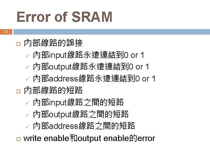
Error of SRAM 27 error 1系列:data_bus_in_signal有一個bit的資料會永遠是 0 (1_1~1_8) or 1 (1_9~2_16) error 2系列:data_bus_out有一個bit的資料會永遠是 0(2_1~2_8) or 1 (2_9~2_16) error 3系列:address_signal有一個bit的資料會永遠是 0(3_1~3_2) or 1 (3_3~3_4) error 4系列:data_bus_in_signal相鄰的bit短路 error 5系列:data_bus_out相鄰的bit短路 error 6系列:address_signal相鄰的bit短路 error 7系列:output enable(oe)和write enable(gw)的錯誤, 7_1是永遠都在寫,7_2是永遠不會寫,7_3是永遠不會讀
SRAM Video 28 play
29 JTAG [kcir] mimi 9126、troychang、JAST、 gomibako、reeetingay
Implementation Overview 30
JTAG File Hierarchy 31
32 RS 232 Buffer File Hierarchy
33 Problems we met
34 萬丈project平地起: JTAG Spec JTAG specification: IEEE 1149. 1 要錢? !
35 萬丈project平地起: JTAG Specification Sources Boundary-Scan Tutorial 2007 (web resource) The Boundary-Scan Handbook (Parker 1992) What is JTAG: Specification details TDO outputs on falling edge TDI inputs on rising clock edge “The last shift occurs on the transition leaving the state” Spec沒有寫到的部份怎麼辦? 真的要照Spec寫……嗎?
Implementation: Fanout 36 Fanout
Implementation: Fanout 37
Implementation: Fanout 38 Solution: 加and gates output. TCK <= Clock. DR and Mode; I 1: for i in 0 to 7 generate input. TCKarray(i) <= input. TCK and Mode; output. TCKarray(i) <= output. TCK and Mode; end generate I 1; data_bus_out_bsc : bsc port map( sram_data_bus_out( i - 1 ), bsc_link_data_bus_out( i ), output. Shiftarray(i mod 8), Mode, output. TCKarray(i mod 8), output. Updatearray(i mod 8), exit_data_bus_out( i - 1 ), bsc_link_data_bus_out( i - 1 ) )
Implementation: Fanout 39
Implementation: Fanout 40 Still don’t know how to make an ‘and’ gate appear……. TCK 1 <= TCK and TCK X TCK 1 <= TCK and 1 X TCK 1 <= TCK and … X TCK 1 <= TCK and Mode O
41 Implementation: 這兩個明明一 樣 CRASH!!!! PASS!!! if oe = '0' and gw = '1' then xxx if gw = '0‘ xxx if gw = '1' then if oe = '0' then xxx elsif gw = '0' then xxx 事後推測可能是有Hazard 修改code時莫明奇妙的好了, 所以當時沒有多做測 試
傳說中的Hazard? ! 42 Functional Timing
傳說中的Hazard? ! 43 Simulation Timing simulation vs Functional Simulation
傳說中的Hazard? ! 44
傳說中的Hazard? ! 45 if(Shift. IRmap = '1') then TDO <= TDO_from_IR; elsif(Shift. DRmap = '1') then TDO <= TDO_from_DR; else TDO <= 'Z'; end if;
傳說中的Hazard? ! 46 罪魁禍首 Clock. DR <= TCK and (Shift. DR_signal or Capture. DR_signal)
傳說中的Hazard? ! 47 Solution 1: Asynchronous Synchronous 不會在value還沒穩定時讀值 Flip flop instead of a latch Solution 2: 把value change的時間從 rising edge換成falling edge 於是在rising edge讀值時,所有值都穩定了 (不會和JTAG spec衝突)
傳說中的Hazard? ! 48 Other symptoms 莫名的多一次shift JTAG與SRAM合併 JTAG與RS 232合併 Conclusion: Hazard是一路伴隨著我們 project從無到有的好朋友 -. -
JTAG Waveform 49
JTAG Waveform 50
51 How to test?
How to test? 52 用C程式(real_tester. c)產生出waveform檔
How to test? 53 Run Simulation
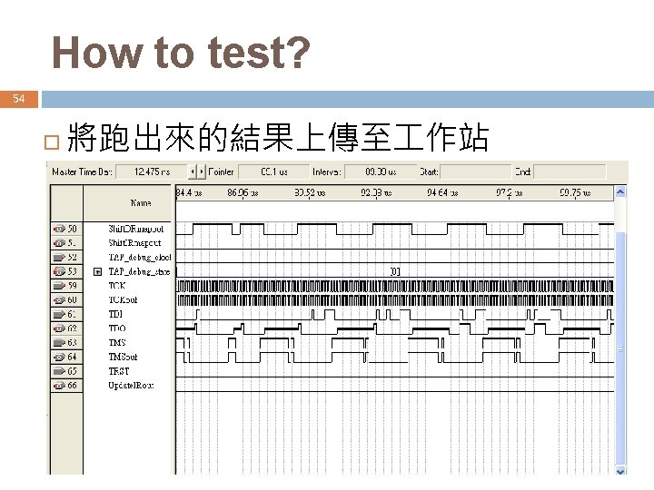
How to test? 55 用另一個C程式(wave_checker. c)去比 對結果
Simulation – Data Bus 56 for (i = 0; i < INTEGER_BIT; i++) { write_board(0, 1 << i); read_board(0, 1 << i); }
Simulation – Data Bus
Simulation – Data Bus
Simulation – Data Bus
Simulation – Data Bus
Simulation – Data Bus
Simulation – Address Bus write_board(0, cpattern); for (i = 0; i < ADDRESS_BIT; i++) read_board(1 << i, pattern);
Simulation – Address Bus
Simulation – Address Bus
Simulation – Others
Reference 67 http: //www. fh-augsburg. de/~hhoegl/proj/usbjtag. html http: //www. boundary-scan. co. uk/page 7. html http: //en. wikipedia. org/wiki/Jtag http: //en. wikipedia. org/wiki/Boundary_scan http: //www. jtag. com/main. php http: //www. csie. ntu. edu. tw/~b 92036/pub/Boundary. Scan_Tutorial_2007. pdf http: //www. csie. ntu. edu. tw/~b 94065/. DSD/blockdiagram. jpg http: //www. jtag. tk/ http: //www. netrino. com/Embedded-Systems/How-To/Memory-Test. Suite-C
Our Website 68 http: //www. csie. ntu. edu. tw/~b 94097/DSD/web site/Home. html