Multilayers and interfaces sami franssilaaalto fi Why multilayers

- Slides: 50

Multilayers and interfaces sami. franssila@aalto. fi

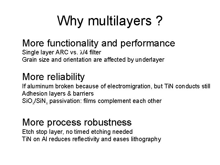
Why multilayers ? More functionality and performance Single layer ARC vs. λ/4 filter Grain size and orientation are affected by underlayer More reliability If aluminum broken because of electromigration, but Ti. N conducts still Adhesion layers & barriers Si. Ox/Si. Nx passivation: films complement each other More process robustness Etch stop layer, no timed etching needed Ti. N on Al reduces reflectivity and eases lithography

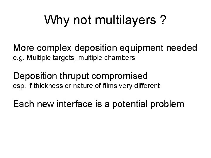
Why not multilayers ? More complex deposition equipment needed e. g. Multiple targets, multiple chambers Deposition thruput compromised esp. if thickness or nature of films very different Each new interface is a potential problem

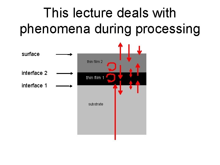
This lecture deals with phenomena during processing surface thin film 2 interface 2 thin film 11 thin interface 1 substrate

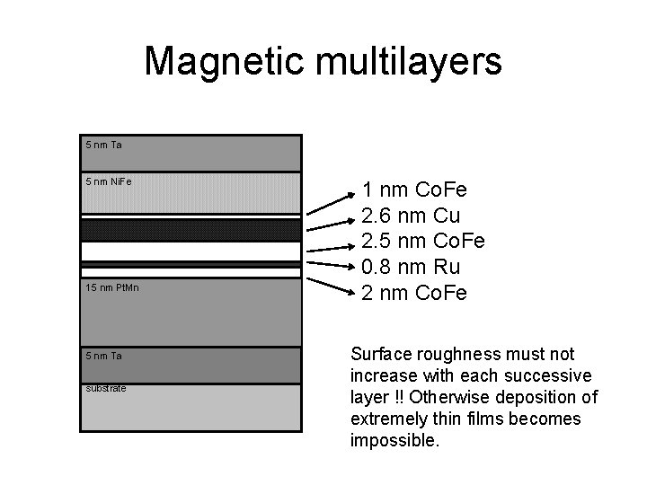
Magnetic multilayers 5 nm Ta 5 nm Ni. Fe 15 nm Pt. Mn 5 nm Ta substrate 1 nm Co. Fe 2. 6 nm Cu 2. 5 nm Co. Fe 0. 8 nm Ru 2 nm Co. Fe Surface roughness must not increase with each successive layer !! Otherwise deposition of extremely thin films becomes impossible.

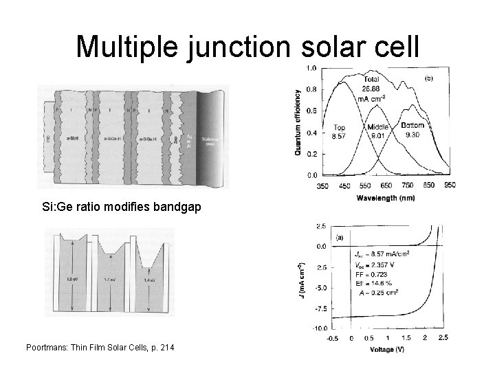
Multiple junction solar cell Si: Ge ratio modifies bandgap Poortmans: Thin Film Solar Cells, p. 214

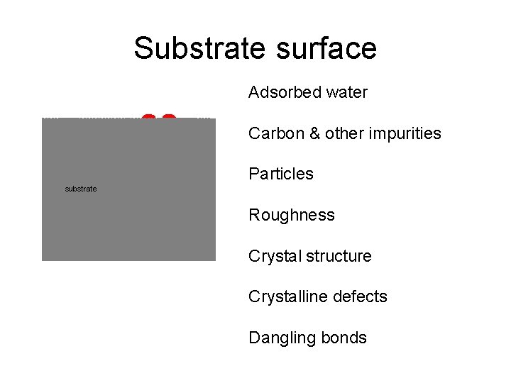
Substrate surface Adsorbed water Carbon & other impurities Particles substrate Roughness Crystal structure Crystalline defects Dangling bonds

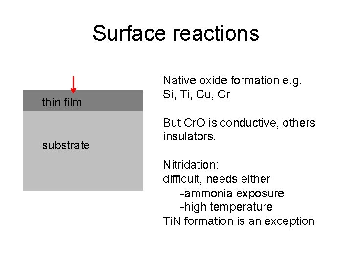
Surface reactions thin film substrate Native oxide formation e. g. Si, Ti, Cu, Cr But Cr. O is conductive, others insulators. Nitridation: difficult, needs either -ammonia exposure -high temperature Ti. N formation is an exception

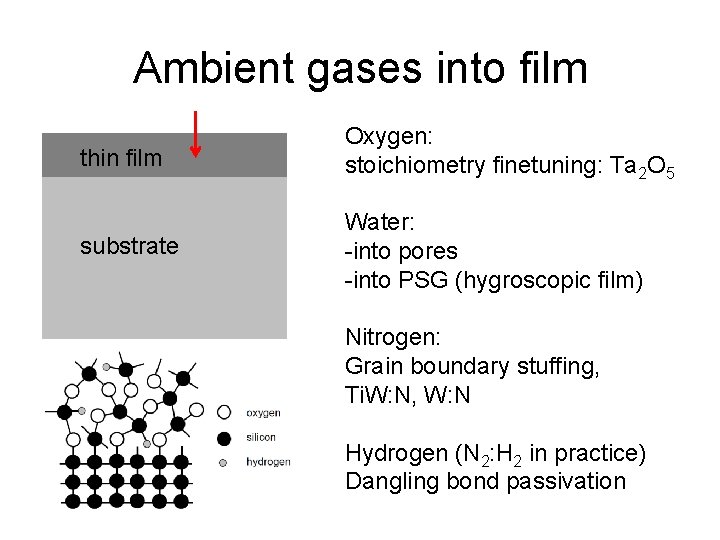
Ambient gases into film thin film Oxygen: stoichiometry finetuning: Ta 2 O 5 substrate Water: -into pores -into PSG (hygroscopic film) Nitrogen: Grain boundary stuffing, Ti. W: N, W: N Hydrogen (N 2: H 2 in practice) Dangling bond passivation

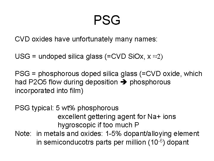
PSG CVD oxides have unfortunately many names: USG = undoped silica glass (=CVD Si. Ox, x ≈2) PSG = phosphorous doped silica glass (=CVD oxide, which had P 2 O 5 flow during deposition phosphorous incorporated into film) PSG typical: 5 wt% phosphorous excellent gettering agent for Na+ ions hygroscopic if too much P Note: in metals and oxides: 1 -5% dopant/alloying element in semiconducotrs parts per million (10 -6) dopant

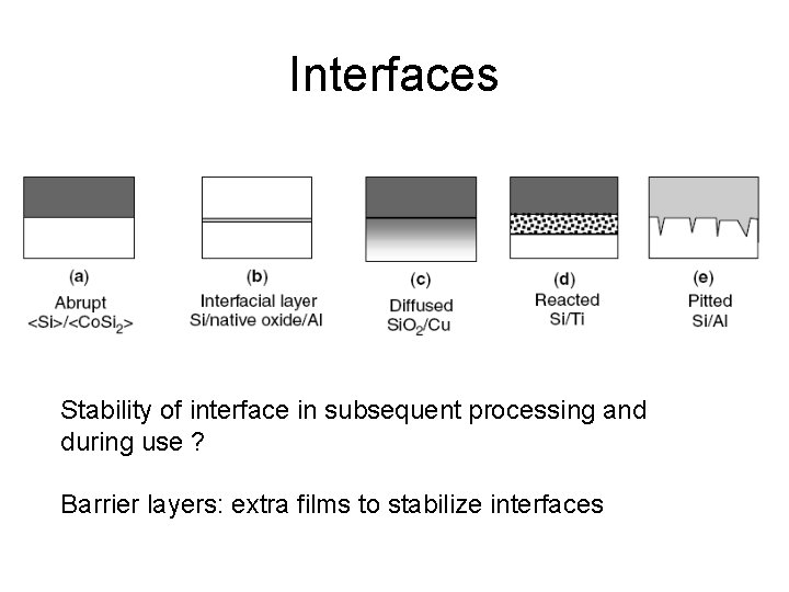
Interfaces Stability of interface in subsequent processing and during use ? Barrier layers: extra films to stabilize interfaces

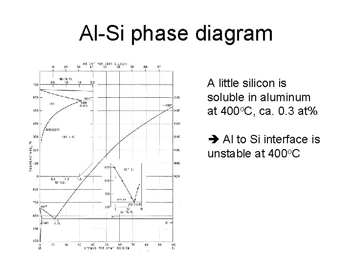
Al-Si phase diagram A little silicon is soluble in aluminum at 400 o. C, ca. 0. 3 at% Al to Si interface is unstable at 400 o. C

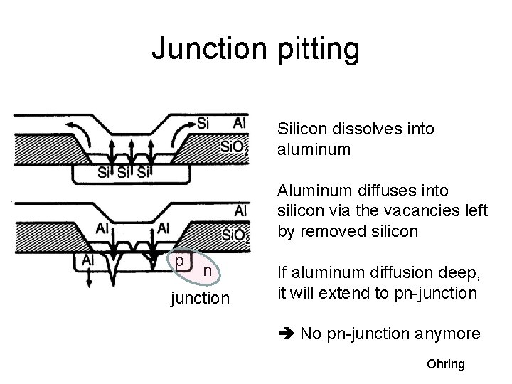
Junction pitting Silicon dissolves into aluminum Aluminum diffuses into silicon via the vacancies left by removed silicon p n junction If aluminum diffusion deep, it will extend to pn-junction No pn-junction anymore Ohring

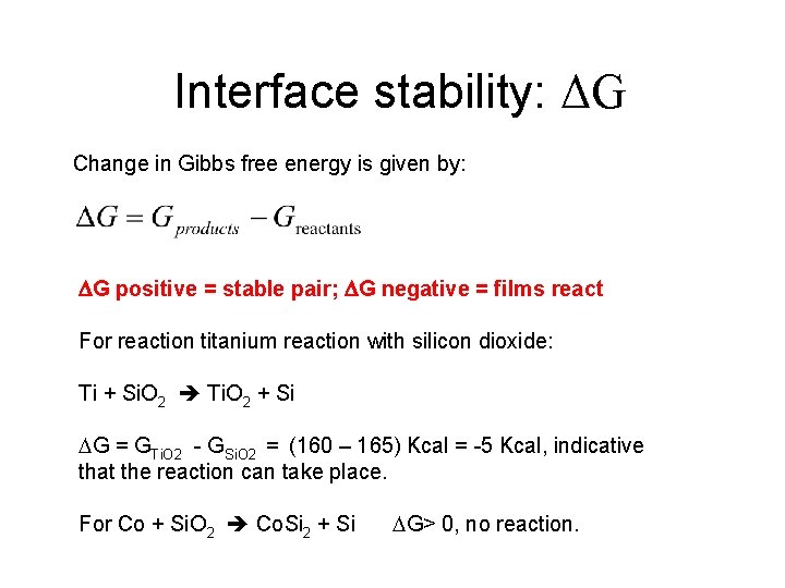
Interface stability: ΔG Change in Gibbs free energy is given by: G positive = stable pair; G negative = films react For reaction titanium reaction with silicon dioxide: Ti + Si. O 2 Ti. O 2 + Si G = GTi. O 2 - GSi. O 2 = (160 – 165) Kcal = -5 Kcal, indicative that the reaction can take place. For Co + Si. O 2 Co. Si 2 + Si G> 0, no reaction.

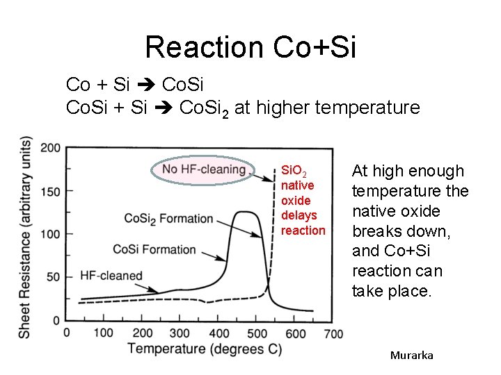
Reaction Co+Si Co + Si Co. Si 2 at higher temperature Si. O 2 native oxide delays reaction At high enough temperature the native oxide breaks down, and Co+Si reaction can take place. Murarka

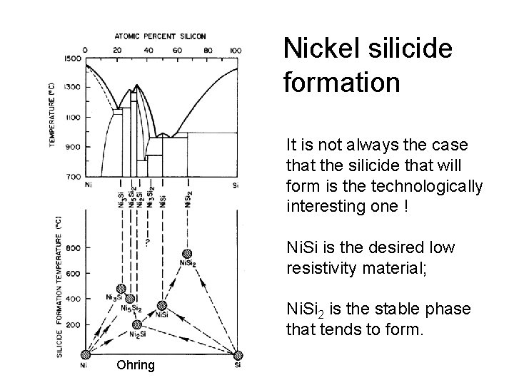
Nickel silicide formation It is not always the case that the silicide that will form is the technologically interesting one ! Ni. Si is the desired low resistivity material; Ni. Si 2 is the stable phase that tends to form. Ohring

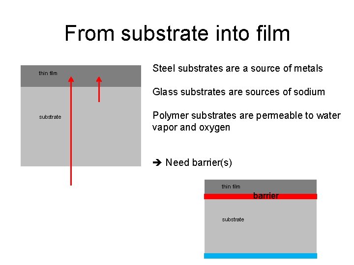
From substrate into film thin film Steel substrates are a source of metals Glass substrates are sources of sodium substrate Polymer substrates are permeable to water vapor and oxygen Need barrier(s) thin film barrier substrate

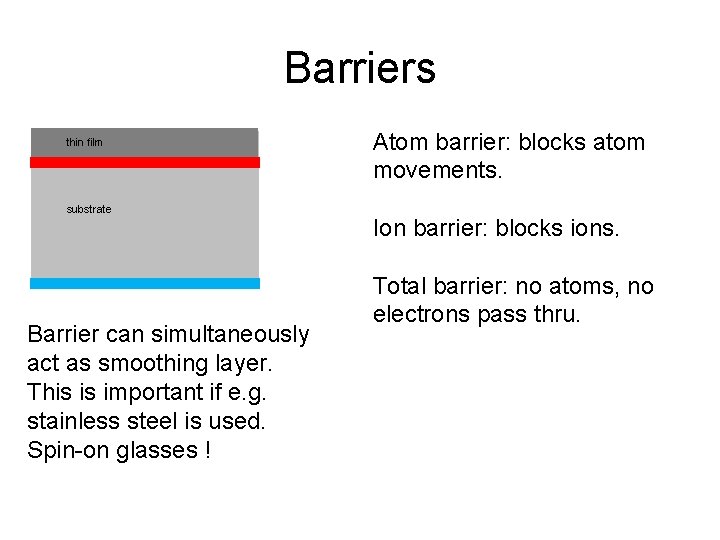
Barriers thin film substrate Barrier can simultaneously act as smoothing layer. This is important if e. g. stainless steel is used. Spin-on glasses ! Atom barrier: blocks atom movements. Ion barrier: blocks ions. Total barrier: no atoms, no electrons pass thru.

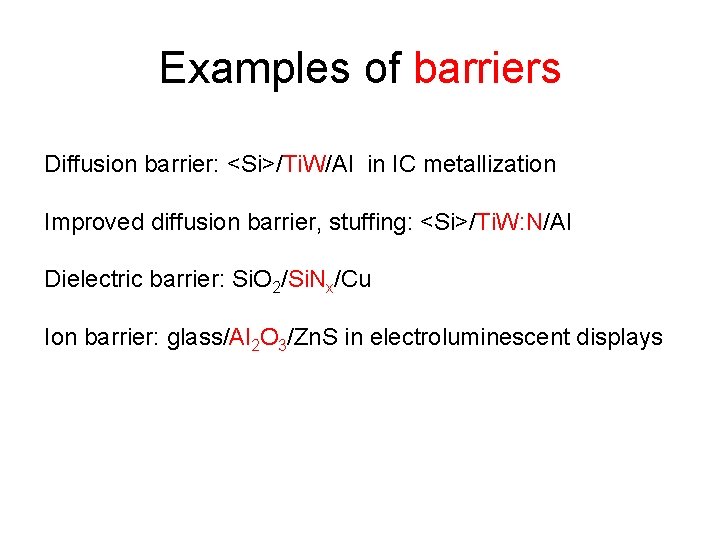
Examples of barriers Diffusion barrier: <Si>/Ti. W/Al in IC metallization Improved diffusion barrier, stuffing: <Si>/Ti. W: N/Al Dielectric barrier: Si. O 2/Si. Nx/Cu Ion barrier: glass/Al 2 O 3/Zn. S in electroluminescent displays

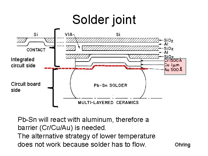
Solder joint Integrated circuit side Circuit board side Pb-Sn will react with aluminum, therefore a barrier (Cr/Cu/Au) is needed. The alternative strategy of lower temperature does not work because solder has to flow. Ohring

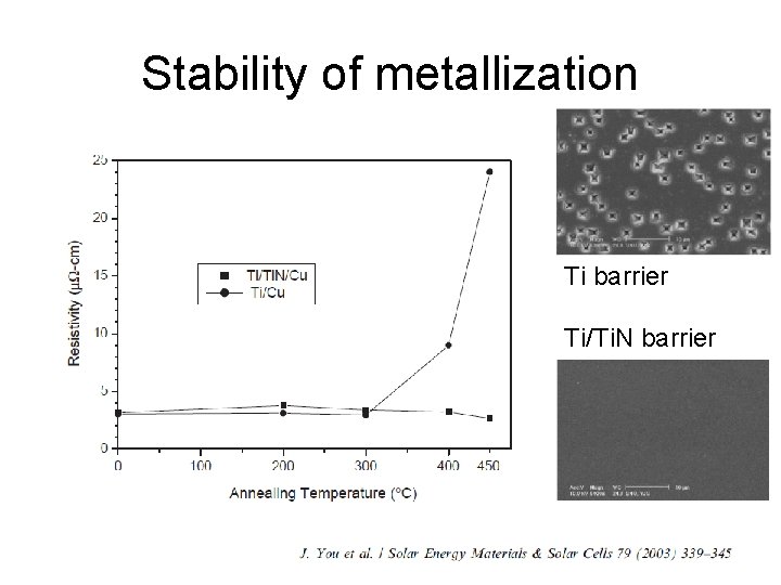
Stability of metallization Ti barrier Ti/Ti. N barrier

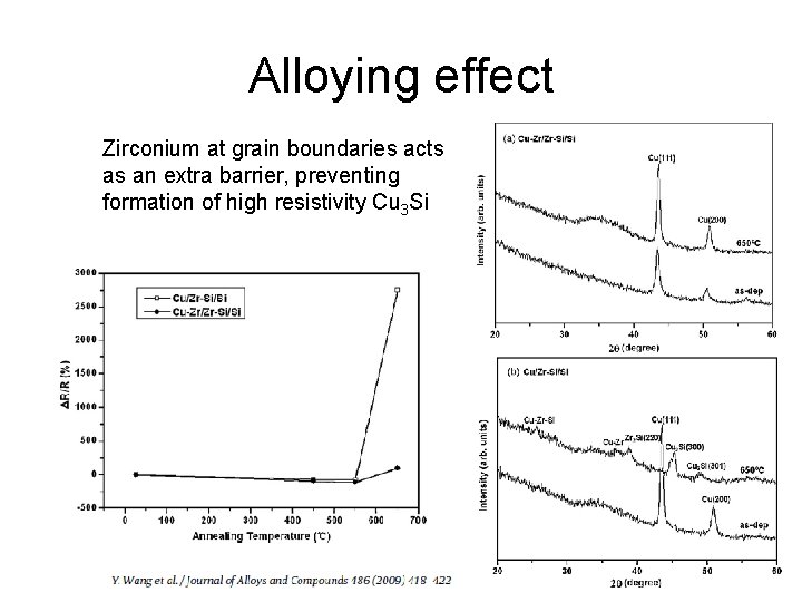
Alloying effect Zirconium at grain boundaries acts as an extra barrier, preventing formation of high resistivity Cu 3 Si

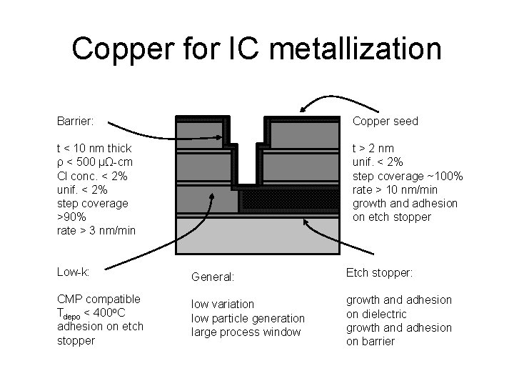
Copper for IC metallization Barrier: Copper seed t < 10 nm thick ρ < 500 µΩ-cm Cl conc. < 2% unif. < 2% step coverage >90% rate > 3 nm/min t > 2 nm unif. < 2% step coverage ~100% rate > 10 nm/min growth and adhesion on etch stopper Low-k: General: Etch stopper: CMP compatible Tdepo < 400 o. C adhesion on etch stopper low variation low particle generation large process window growth and adhesion on dielectric growth and adhesion on barrier

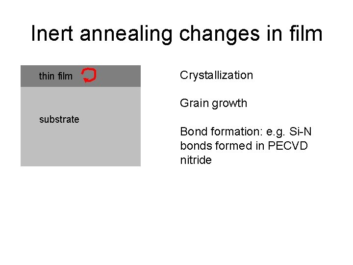
Inert annealing changes in film thin film Crystallization Grain growth substrate Bond formation: e. g. Si-N bonds formed in PECVD nitride

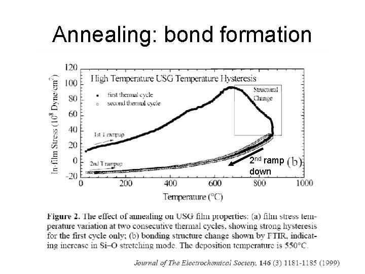
Annealing: bond formation 2 nd ramp down

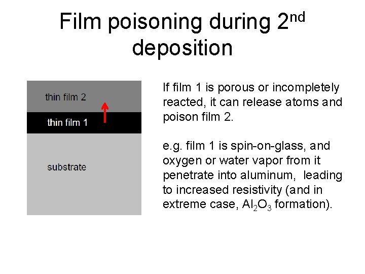
Film poisoning during deposition nd 2 If film 1 is porous or incompletely reacted, it can release atoms and poison film 2. e. g. film 1 is spin-on-glass, and oxygen or water vapor from it penetrate into aluminum, leading to increased resistivity (and in extreme case, Al 2 O 3 formation).

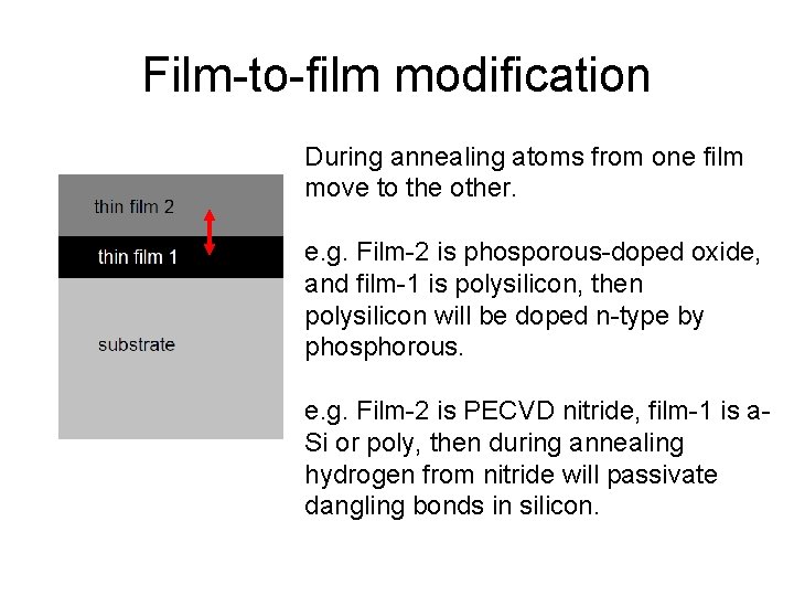
Film-to-film modification During annealing atoms from one film move to the other. e. g. Film-2 is phosporous-doped oxide, and film-1 is polysilicon, then polysilicon will be doped n-type by phosphorous. e. g. Film-2 is PECVD nitride, film-1 is a. Si or poly, then during annealing hydrogen from nitride will passivate dangling bonds in silicon.

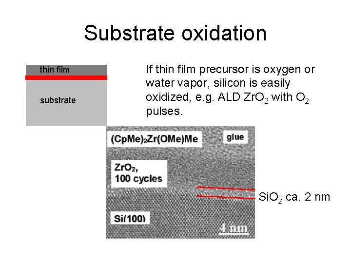
Substrate oxidation thin film substrate If thin film precursor is oxygen or water vapor, silicon is easily oxidized, e. g. ALD Zr. O 2 with O 2 pulses. Si. O 2 ca. 2 nm

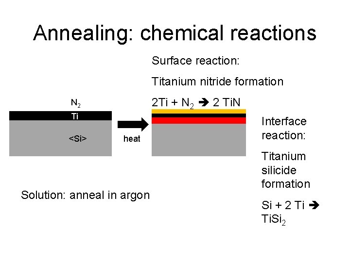
Annealing: chemical reactions Surface reaction: Titanium nitride formation 2 Ti + N 2 2 Ti. N N 2 Ti <Si> heat Solution: anneal in argon Interface reaction: Titanium silicide formation Si + 2 Ti Ti. Si 2

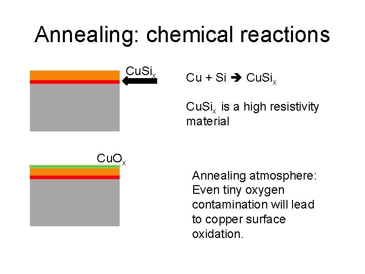
Annealing: chemical reactions Cu. Six Cu + Si Cu. Six is a high resistivity material Cu. Ox Annealing atmosphere: Even tiny oxygen contamination will lead to copper surface oxidation.

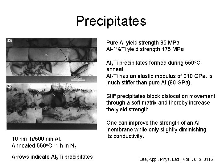
Precipitates Pure Al yield strength 95 MPa Al-1%Ti yield strength 175 MPa Al 3 Ti precipitates formed during 550 o. C anneal. Al 3 Ti has an elastic modulus of 210 GPa, is much stiffer than pure Al (60 GPa). Stiff precipitates block dislocation movement through a soft matrix and thereby increase the yield strength. 10 nm Ti/500 nm Al, Annealed 550 o. C, 1 h in N 2 Arrows indicate Al 3 Ti precipitates One can improve the strength of an Al membrane while only slightly diminishing its conductivity. Lee, Appl. Phys. Lett. , Vol. 76, p. 3415

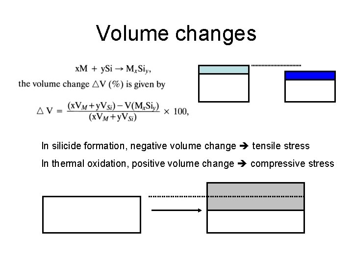
Volume changes In silicide formation, negative volume change tensile stress In thermal oxidation, positive volume change compressive stress

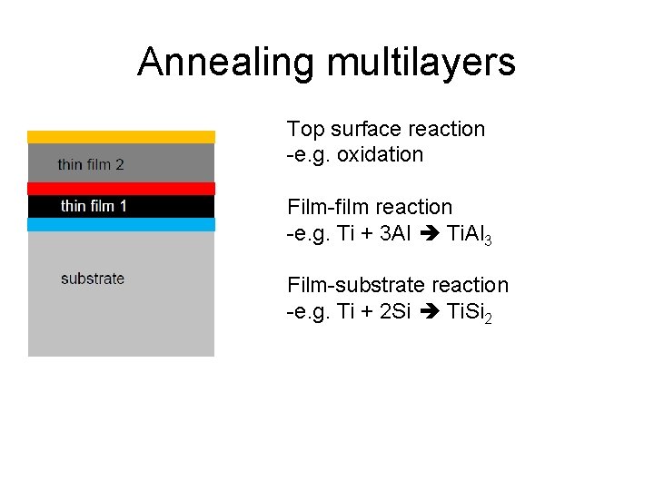
Annealing multilayers Top surface reaction -e. g. oxidation Film-film reaction -e. g. Ti + 3 Al Ti. Al 3 Film-substrate reaction -e. g. Ti + 2 Si Ti. Si 2

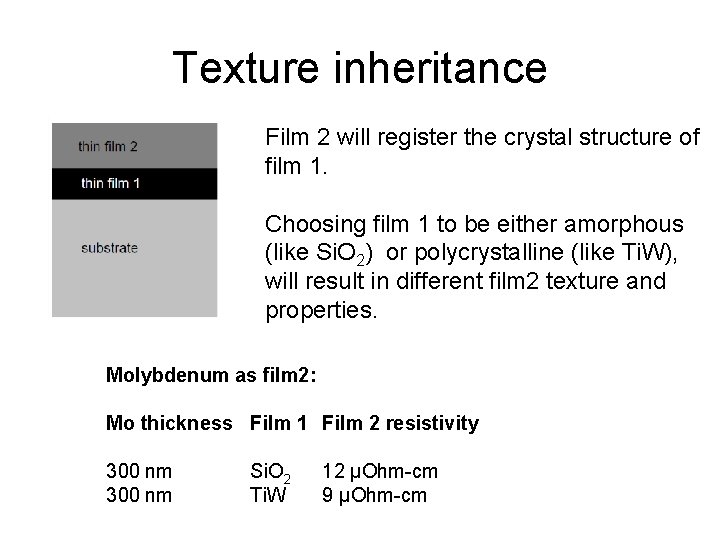
Texture inheritance Film 2 will register the crystal structure of film 1. Choosing film 1 to be either amorphous (like Si. O 2) or polycrystalline (like Ti. W), will result in different film 2 texture and properties. Molybdenum as film 2: Mo thickness Film 1 Film 2 resistivity 300 nm Si. O 2 Ti. W 12 µOhm-cm 9 µOhm-cm

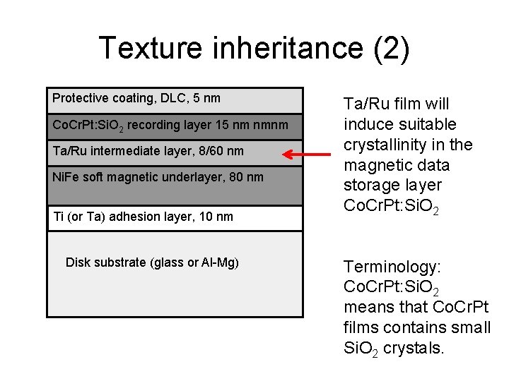
Texture inheritance (2) Protective coating, DLC, 5 nm Co. Cr. Pt: Si. O 2 recording layer 15 nm nmnm Ta/Ru intermediate layer, 8/60 nm Ni. Fe soft magnetic underlayer, 80 nm Ti (or Ta) adhesion layer, 10 nm Disk substrate (glass or Al-Mg) Ta/Ru film will induce suitable crystallinity in the magnetic data storage layer Co. Cr. Pt: Si. O 2 Terminology: Co. Cr. Pt: Si. O 2 means that Co. Cr. Pt films contains small Si. O 2 crystals.

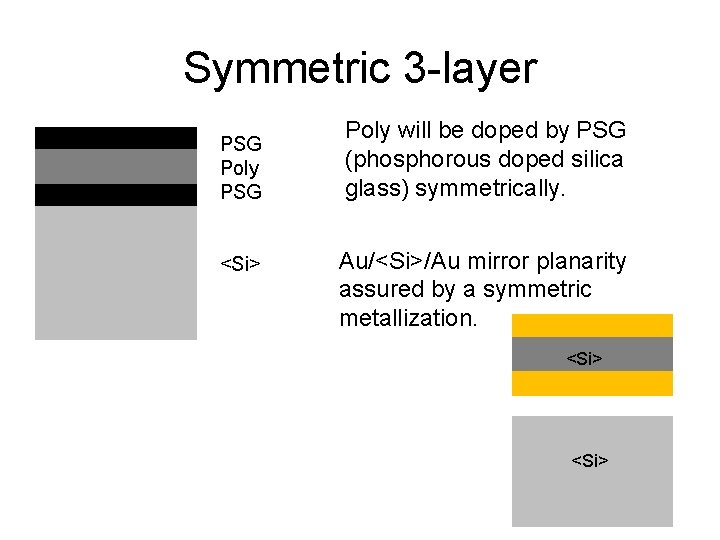
Symmetric 3 -layer PSG Poly PSG <Si> Poly will be doped by PSG (phosphorous doped silica glass) symmetrically. Au/<Si>/Au mirror planarity assured by a symmetric metallization. <Si>

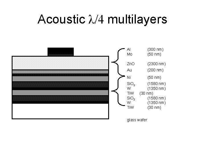
Acoustic λ/4 multilayers Al Mo (300 nm) (50 nm) Zn. O (2300 nm) Au (200 nm) Ni (50 nm) Si. O 2 W Ti. W (1580 nm) (1350 nm) (30 nm) glass wafer

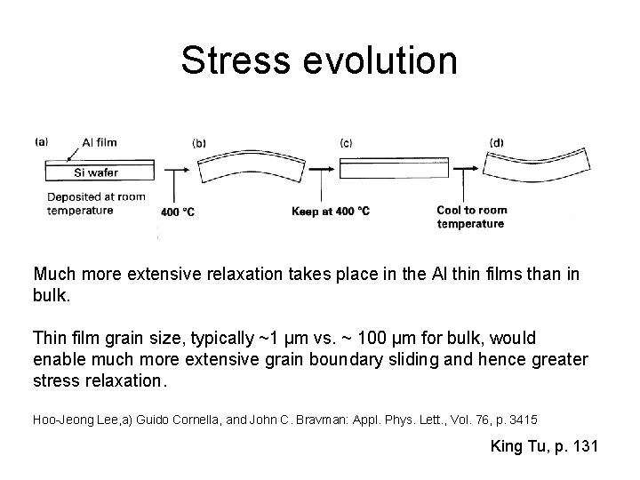
Stress evolution Much more extensive relaxation takes place in the Al thin films than in bulk. Thin film grain size, typically ~1 µm vs. ~ 100 µm for bulk, would enable much more extensive grain boundary sliding and hence greater stress relaxation. Hoo-Jeong Lee, a) Guido Cornella, and John C. Bravman: Appl. Phys. Lett. , Vol. 76, p. 3415 King Tu, p. 131

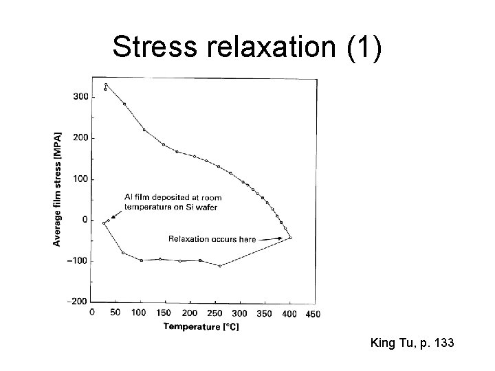
Stress relaxation (1) King Tu, p. 133

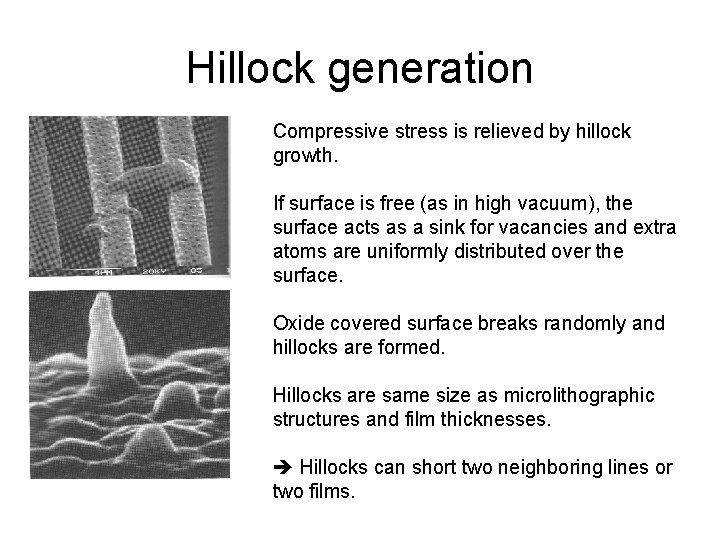
Hillock generation Compressive stress is relieved by hillock growth. If surface is free (as in high vacuum), the surface acts as a sink for vacancies and extra atoms are uniformly distributed over the surface. Oxide covered surface breaks randomly and hillocks are formed. Hillocks are same size as microlithographic structures and film thicknesses. Hillocks can short two neighboring lines or two films.

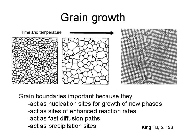
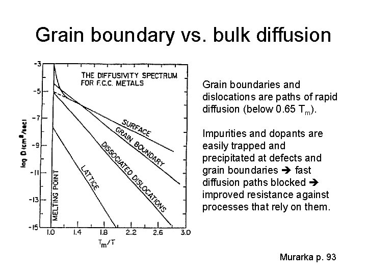
Grain growth Grain boundaries important because they: -act as nucleation sites for growth of new phases -act as sites of enhanced reaction rates -act as fast diffusion paths -act as precipitation sites King Tu, p. 193

Grain boundary vs. bulk diffusion Grain boundaries and dislocations are paths of rapid diffusion (below 0. 65 Tm). Impurities and dopants are easily trapped and precipitated at defects and grain boundaries fast diffusion paths blocked improved resistance against processes that rely on them. Murarka p. 93

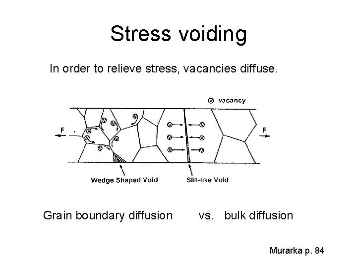
Stress voiding In order to relieve stress, vacancies diffuse. Grain boundary diffusion vs. bulk diffusion Murarka p. 84

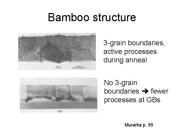
Bamboo structure 3 -grain boundaries, active processes during anneal No 3 -grain boundaries fewer processes at GBs Murarka p. 99

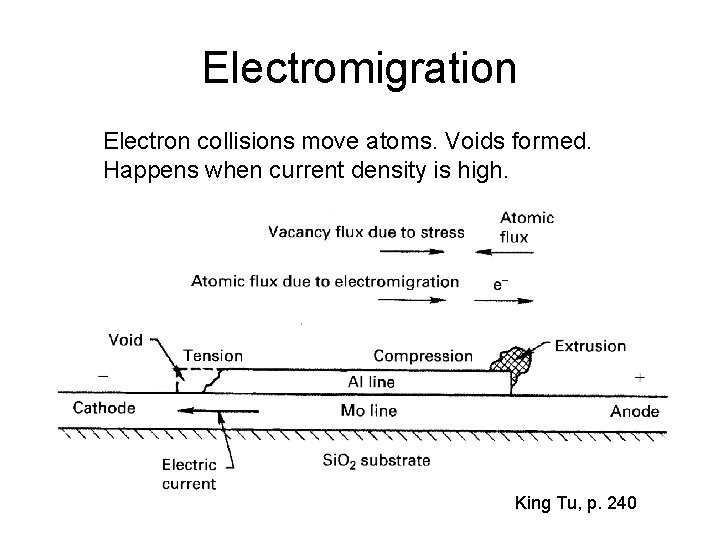
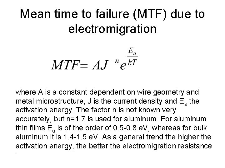
Electromigration Electron collisions move atoms. Voids formed. Happens when current density is high. King Tu, p. 240

Mean time to failure (MTF) due to electromigration where A is a constant dependent on wire geometry and metal microstructure, J is the current density and Ea the activation energy. The factor n is not known very accurately, but n=1. 7 is used for aluminum. For aluminum thin films Ea is of the order of 0. 5 -0. 8 e. V, whereas for bulk aluminum it is 1. 4 -1. 5 e. V. As a general trend the higher the activation energy, the better the electromigration resistance.

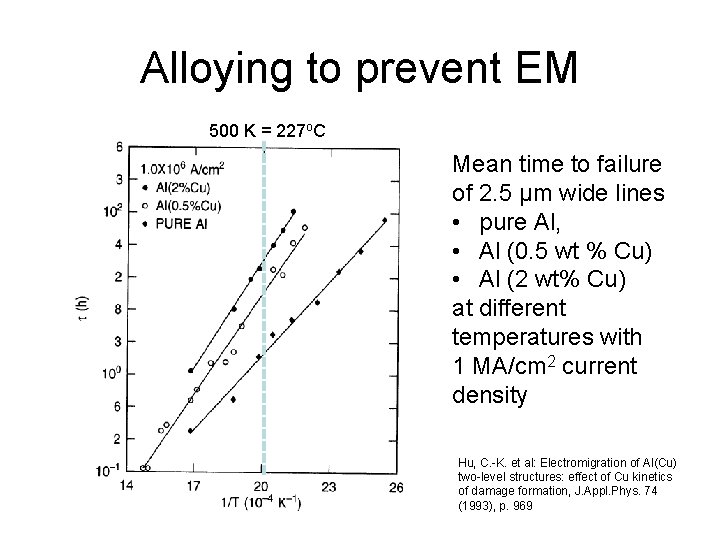
Alloying to prevent EM 500 K = 227 o. C Mean time to failure of 2. 5 µm wide lines • pure Al, • Al (0. 5 wt % Cu) • Al (2 wt% Cu) at different temperatures with 1 MA/cm 2 current density Hu, C. -K. et al: Electromigration of Al(Cu) two-level structures: effect of Cu kinetics of damage formation, J. Appl. Phys. 74 (1993), p. 969

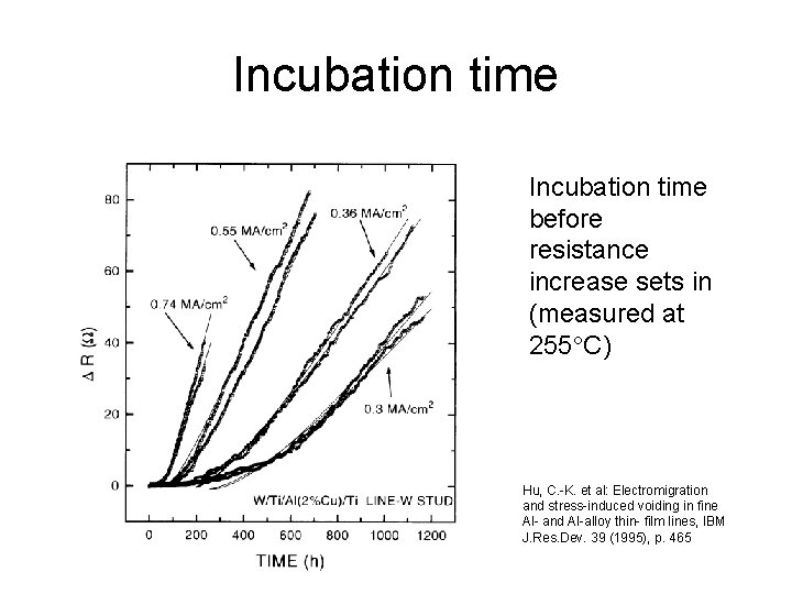
Incubation time before resistance increase sets in (measured at 255 C) Hu, C. -K. et al: Electromigration and stress-induced voiding in fine Al- and Al-alloy thin- film lines, IBM J. Res. Dev. 39 (1995), p. 465

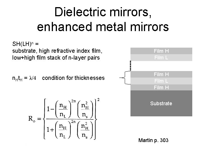
Dielectric mirrors, enhanced metal mirrors SH(LH)n = substrate, high refractive index film, low+high film stack of n-layer pairs n. Ht. H = λ/4 condition for thicknesses Film H Film L Film H Substrate Martin p. 303

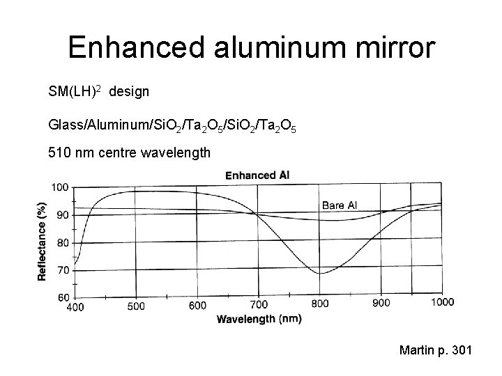
Enhanced aluminum mirror SM(LH)2 design Glass/Aluminum/Si. O 2/Ta 2 O 5 510 nm centre wavelength Martin p. 301