FPGA PRESENTATION Jody Everett General5 minutes Xilinx specific50


- Slides: 36

FPGA PRESENTATION Jody Everett General-5 minutes Xilinx specific-50 to 60 minutes

FPGA Users Medical equipment producers-Lower cost than ASICs in low volume production. Example Beckman-Coulter Test Instrument manufacturers-Lower cost than ASICs in low volume production. Examples-Agilent, Keysight, National Instrument. Research institutions-low cost and re-programmability. Defense contractors-easily changeable systems. Example. Raytheon

FPGA users-continued Semiconductor Companies-re-programmability-emulation Consumer Electronics Companies-Reprogrammabilityprototyping and first production. Telecommunications companies-re-programmability-Base stations can easily adapt to new standards. Specialized manufacturers-makers of business connection technology-Polycom

FPGA types SRAM based-Xilinx, Altera(Intel), Microsemi, Lattice Semiconductor. The program in the SRAM based FPGAs is lost upon power down and must be re-loaded each power up. SRAM based FPGAs usually use more power than flash based. Flash Based – Microsemi. The program is not lost in power down. Lower power than SRAM based FPGAs. Microsemi also produces SRAM based FPGAs Antifuse based- Micro. Semi -one time programmable. These are usually used for security reasons. Also low power.

Xilinx specific information Four Main lines-Virtex, Kintix, Artix, and Spartan. The Virtex line is the most expensive and has more features than the other lines. Members of the Virtex line include Virtex 4, Virtex 5, Virtex 6, Virtex 7 and Virtex Ultrascale. Members of the Kintix line include the Kintix 7 and the Kintix Ultrascale Members of the Spartan line include Spartan 6, and Spartan 7. The Spartan 3 series is obsolete. The only member of the Artix line is the Artix 7. Xilinx also produces the Zynq series of programmable SOC Ics. These contain hard ARM cores, A 9 and A 53.

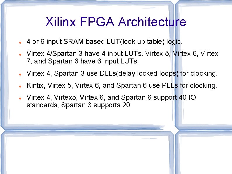
Xilinx FPGA Architecture 4 or 6 input SRAM based LUT(look up table) logic. Virtex 4/Spartan 3 have 4 input LUTs. Virtex 5, Virtex 6, Virtex 7, and Spartan 6 have 6 input LUTs. Virtex 4, Spartan 3 use DLLs(delay locked loops) for clocking. Kintix, Virtex 5, Virtex 6, and Spartan 6 use PLLs for clocking. Virtex 4, Virtex 5, Virtex 6, and Spartan 6 support 40 IO standards, Spartan 3 supports 20

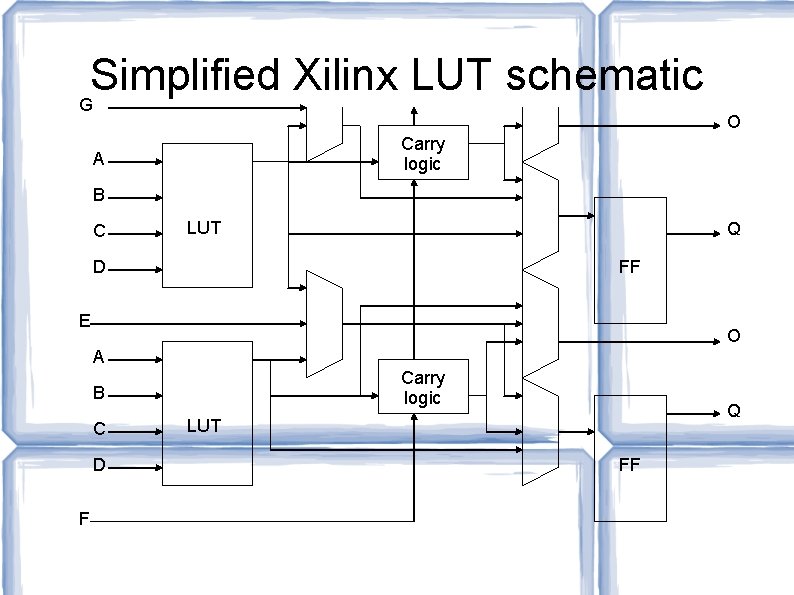
Simplified Xilinx LUT schematic G O Carry logic A B C LUT Q D FF E O A Carry logic B C D F Q LUT FF

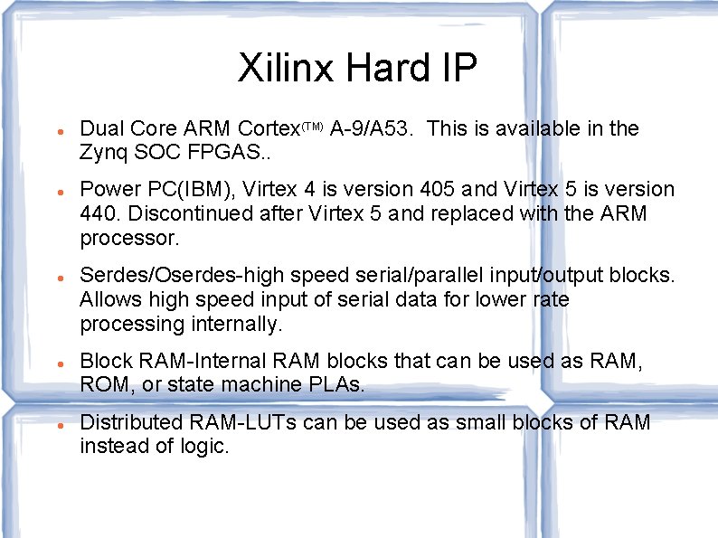
Xilinx Hard IP Dual Core ARM Cortex(TM) A-9/A 53. This is available in the Zynq SOC FPGAS. . Power PC(IBM), Virtex 4 is version 405 and Virtex 5 is version 440. Discontinued after Virtex 5 and replaced with the ARM processor. Serdes/Oserdes-high speed serial/parallel input/output blocks. Allows high speed input of serial data for lower rate processing internally. Block RAM-Internal RAM blocks that can be used as RAM, ROM, or state machine PLAs. Distributed RAM-LUTs can be used as small blocks of RAM instead of logic.

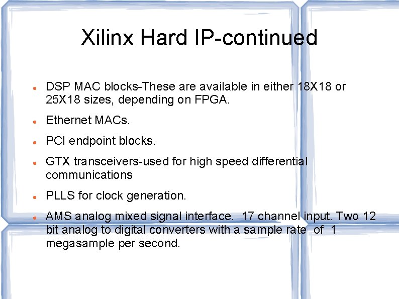
Xilinx Hard IP-continued DSP MAC blocks-These are available in either 18 X 18 or 25 X 18 sizes, depending on FPGA. Ethernet MACs. PCI endpoint blocks. GTX transceivers-used for high speed differential communications PLLS for clock generation. AMS analog mixed signal interface. 17 channel input. Two 12 bit analog to digital converters with a sample rate of 1 megasample per second.

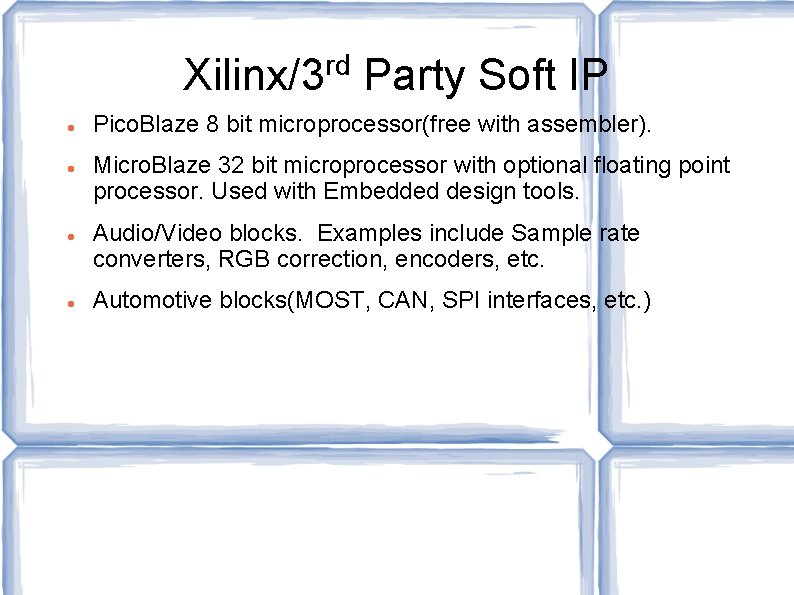
rd Xilinx/3 Party Soft IP Pico. Blaze 8 bit microprocessor(free with assembler). Micro. Blaze 32 bit microprocessor with optional floating point processor. Used with Embedded design tools. Audio/Video blocks. Examples include Sample rate converters, RGB correction, encoders, etc. Automotive blocks(MOST, CAN, SPI interfaces, etc. )

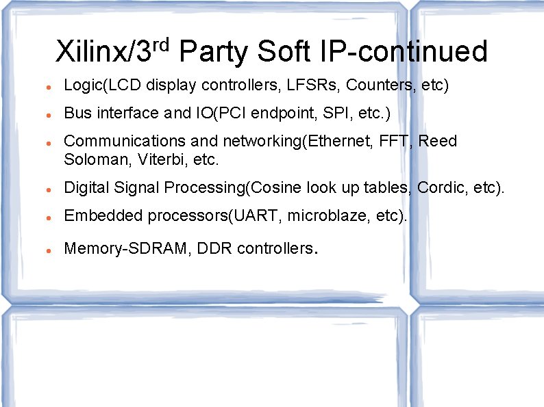
rd Xilinx/3 Party Soft IP-continued Logic(LCD display controllers, LFSRs, Counters, etc) Bus interface and IO(PCI endpoint, SPI, etc. ) Communications and networking(Ethernet, FFT, Reed Soloman, Viterbi, etc. Digital Signal Processing(Cosine look up tables, Cordic, etc). Embedded processors(UART, microblaze, etc). Memory-SDRAM, DDR controllers.

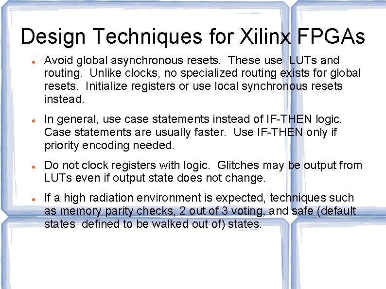
Design Techniques for Xilinx FPGAs Avoid global asynchronous resets. These use LUTs and routing. Unlike clocks, no specialized routing exists for global resets. Initialize registers or use local synchronous resets instead. In general, use case statements instead of IF-THEN logic. Case statements are usually faster. Use IF-THEN only if priority encoding needed. Do not clock registers with logic. Glitches may be output from LUTs even if output state does not change. If a high radiation environment is expected, techniques such as memory parity checks, 2 out of 3 voting, and safe (default states defined to be walked out of) states.

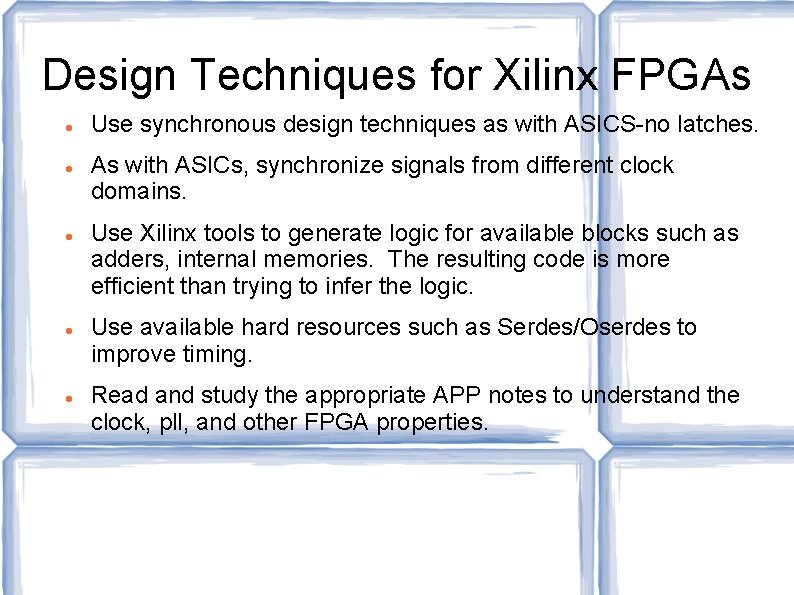
Design Techniques for Xilinx FPGAs Use synchronous design techniques as with ASICS-no latches. As with ASICs, synchronize signals from different clock domains. Use Xilinx tools to generate logic for available blocks such as adders, internal memories. The resulting code is more efficient than trying to infer the logic. Use available hard resources such as Serdes/Oserdes to improve timing. Read and study the appropriate APP notes to understand the clock, pll, and other FPGA properties.

Design Techniques for Xilinx FPGAs In general route input/output buses on the left and right sides of the FPGA(LSB at the bottom). Route control signals to top or bottom. Check FPGA data sheet to verify, some have pins in columns(Virtex 6 and others) Use pipelining or logic duplication to improve timing. Unlike ASICS, logic is not wasted as long as the FPGA is not full. Aim for 80% FPGA utilization. More than that is very hard to achieve. Less is wasteful and a smaller(cheaper) FPGA could possibly have been chosen. In general, use the Xilinx Planahead© tool to plan the layout and pinout of the Xilinx FPGA you have chosen.

Xilinx tools ISE webpack-contains design entry, XST synthesis, mapping, place and route, and timing tools(free-but only covers some Xilinx FPGAs). A full version of ISE can be purchased to cover all Xilinx FPGAs. Vivado-Updated version of ISE. Friendlier to TCL and partial design iterations. Also uses industry standard input files. Synopsys type constraint files, not Xilinx UCF. Accepts System Verilog. ISIM-Xilinx Verilog/VHDL simulator. Mentor Graphics Modelsim also promoted. Plan-ahead-Pin planning, signal integrity, and implementation guidance tool. Useful for timing analysis also. Chipscope-Debugging tool. This works by adding a small amount of logic in the FPGA to output the internal states of the FPGA via JTAG.

Xilinx tools Embedded Development Kit-Software/Hardware development kit for use with ARM, PPC and microblaze processors. System Generator for DSP-Maps Mat. Lab(trademark of Mathworks) to Xilinx usable logic. Boards and Kits-Xilinx and other manufacturers offer several boards and kits. Xilinx boards and kits usually contain buttons, switches, VGA ports, UART ports, USB ports and other connectors. Some contain A/D and D/A converters.

Xilinx tools Boards and kits continued. -A new type of board is the FPGA Mezzanine card. This card is designed to a standard that allows direct connection to a desktop PC via the PCI port.

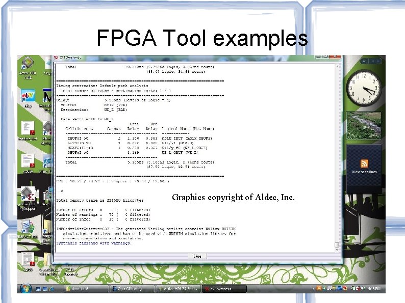
FPGA Tool examples Graphics copyright of Aldec, Inc.

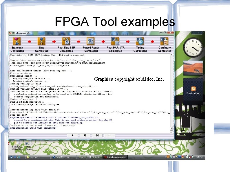
FPGA Tool examples Graphics copyright of Aldec, Inc.

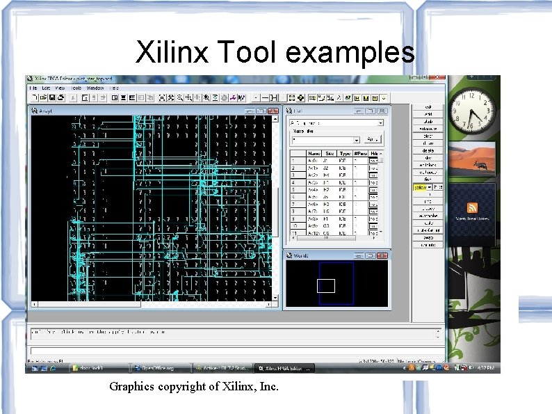
Xilinx Tool examples Graphics copyright of Xilinx, Inc.

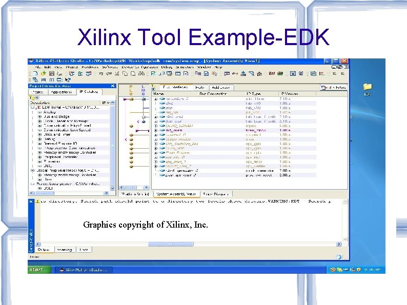
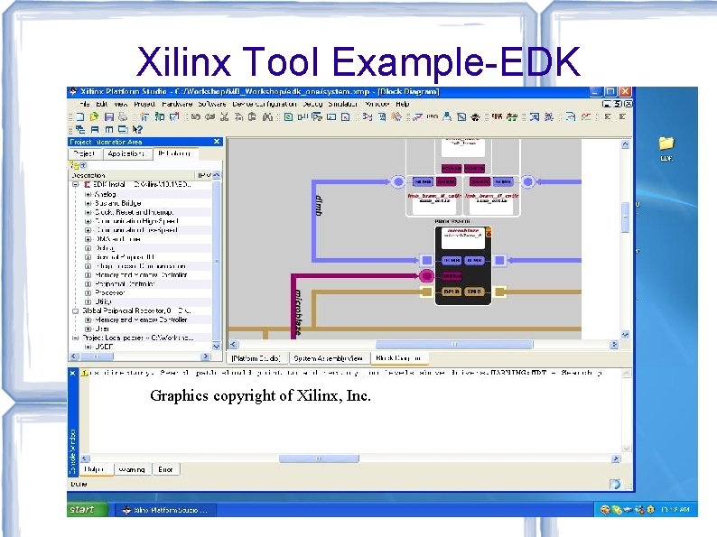
Xilinx Tool Example-EDK System builder • Builds system around Xilinx embedded processors-Microblaze or ARM. Not sure if PPC is supported at present. • Contains Xilinx IP library. • Enables user IP to connect to processor bus, generates bus connection code(either Verilog or VHDL. User then generates desired logic. • Enables easy setting of addressing and ports. • System assembly of block diagram view. • Contains Software Development Kit.

Xilinx Tool Example-EDK Graphics copyright of Xilinx, Inc.

Xilinx Tool Example-EDK Graphics copyright of Xilinx, Inc.

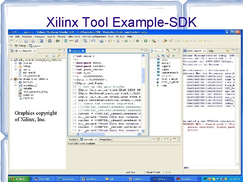
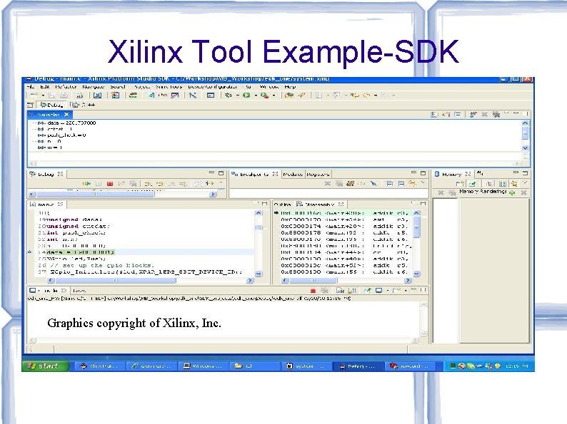
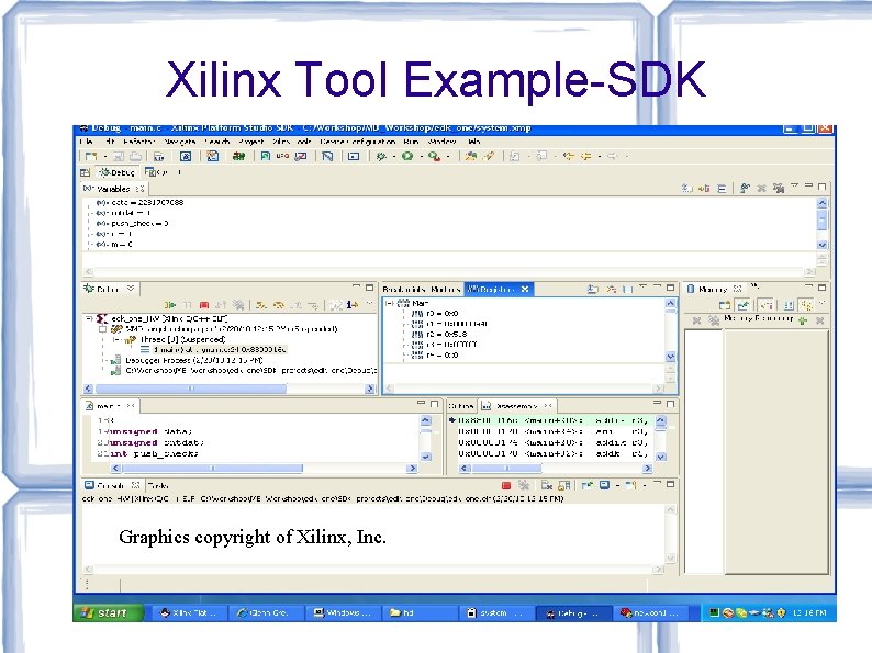
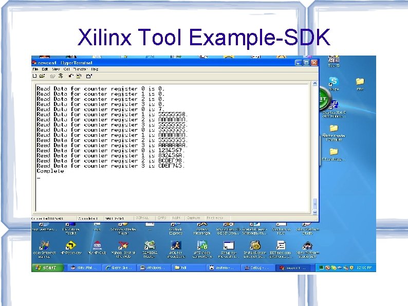
Xilinx Tool Examples-SDK Software Development Kit for EDK • Used to develop software. • Debugger included. • Debugger allows breakpoints, code disassembly, register, and module views. • Debugger allows single stepping, and step over of code.

Xilinx Tool Example-SDK Graphics copyright of Xilinx, Inc.

Xilinx Tool Example-SDK Graphics copyright of Xilinx, Inc.

Xilinx Tool Example-SDK Graphics copyright of Xilinx, Inc.

Xilinx Tool Example-SDK

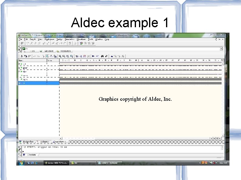
Third Party Tools Synopsys Synplicity-Synthesis tool. Synopsys also sells HAPS prototyping boards. Mentor Modelsim-HDL simulator recommended by Xilinx and Altera. Mentor also offers a Synthesis tool. Cadence-Board Design Solutions. Digilent-Boards and kits. Avnet-Boards and kits. Aldec-HDL simulator. This is one of the simulators that I have used. Examples following. Standard IC grade Mentor Graphics, Synopsys and Cadence asic logic simulators are also applicable, but cost more than FPGA logic simulators

Aldec example 1 Graphics copyright of Aldec, Inc.

Aldec Example II Graphics copyright of Aldec, Inc.

Other FPGA vendors-Altera • Second in market share to Xilinx. Now owned by Intel. Xilinx and Altera control 80% of the FPGA market from the information that I have. • Markets Stratix(High End) , Arria(Mid Range), and Cyclone(Low Cost) devices. The also carry the MAX 10 series flash based FPGA. This FPGA also has analog interface capability similar to Xilinx. The capability of the analog interface depends on the MAX 10 FPGA chosen. • Hardware and software offerings similar to Xilinx. • One difference is that an ARM core is available on each of the Altera lines. The Cyclone and Arria series are available with the ARM 9 core. The Stratix series is available with the ARM 53 core.

Other FPGA vendors-Microsemi • Carry FPGAs and many other types of ICs. Unlike Altera and Xilinx, FPGAs are not their only business. • Markets the Smartfusion(high end), Igloo(low end), Pro. ASIC 3, and RTG 4(radiation hard) FPGAs. • The Igloo series contain both low power and flash based FPGAs. • The ARM Cortex M 1 core is available on the Smartfusion, Pro. ASIC 3, and Igloo series of FPGAs. • The RTG 4 series is flash based as well as radiation hardened.

Other Resources-opencores. org Source for IP cores with General Purpose license. Check with legal department before using these in a product. From discussions that I have had with users(and my own experience), quality of cores varies from excellent to poor. I have experience with the VGA_LCD core. It is of good quality with good documentation. Cores include processors, DSP, Interfaces(I 2 C, SPI), Audio(I 2 S, SPDIF), video/graphics(VGA controllers, JPEG encoders, LCD controllers)

Training • Altera/Xilinx websites-Both have many white papers, app notes and Webinars. • Instructor led training. Both Xilinx and Altera have this available. For Xilinx, the website for instructor led training(Texas) is www. fastertechnology. com.

Late Breaking News Achronix • Achronix Semiconductor has announced Speedcore e. FPGA cores that can be supplied to SOC designers. • GDSII(Layout) and programming tools supplied for digital processes. • Architecture similar to other RAM based FPGAS. • Allows users custom SOC processors and other logic to be mated to FPGA logic.