EE 895 KR Advanced VLSI Design Kaushik Roy
- Slides: 68
EE 895 KR Advanced VLSI Design Kaushik Roy Purdue University Dept. of ECE kaushik@purdue. edu
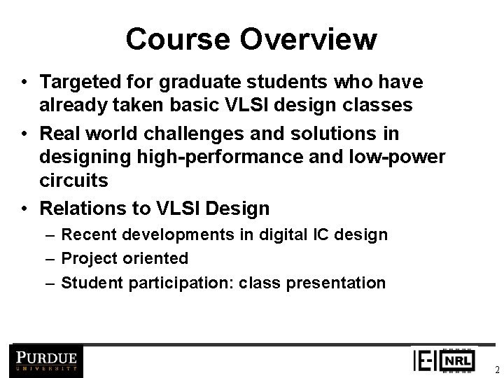
Course Overview • Targeted for graduate students who have already taken basic VLSI design classes • Real world challenges and solutions in designing high-performance and low-power circuits • Relations to VLSI Design – Recent developments in digital IC design – Project oriented – Student participation: class presentation 2
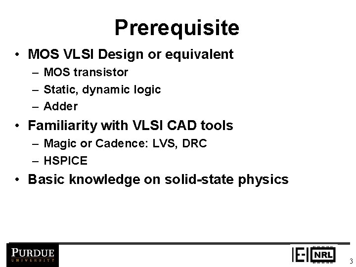
Prerequisite • MOS VLSI Design or equivalent – MOS transistor – Static, dynamic logic – Adder • Familiarity with VLSI CAD tools – Magic or Cadence: LVS, DRC – HSPICE • Basic knowledge on solid-state physics 3
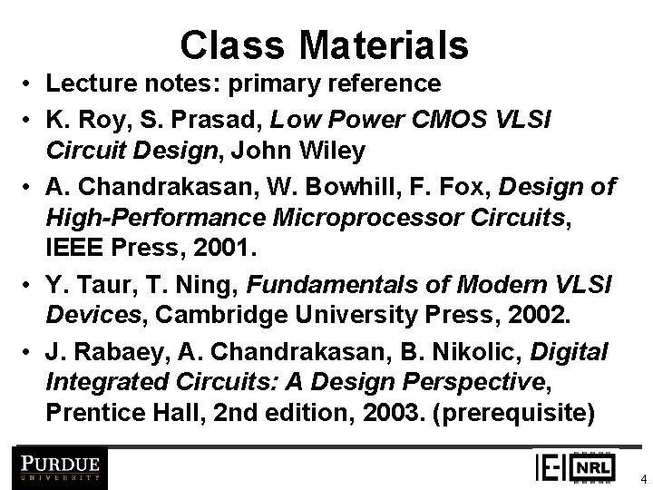
Class Materials • Lecture notes: primary reference • K. Roy, S. Prasad, Low Power CMOS VLSI Circuit Design, John Wiley • A. Chandrakasan, W. Bowhill, F. Fox, Design of High-Performance Microprocessor Circuits, IEEE Press, 2001. • Y. Taur, T. Ning, Fundamentals of Modern VLSI Devices, Cambridge University Press, 2002. • J. Rabaey, A. Chandrakasan, B. Nikolic, Digital Integrated Circuits: A Design Perspective, Prentice Hall, 2 nd edition, 2003. (prerequisite) 4
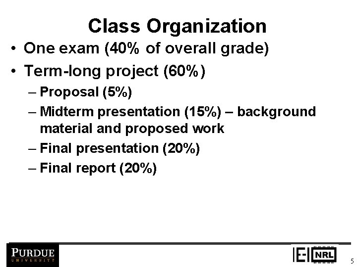
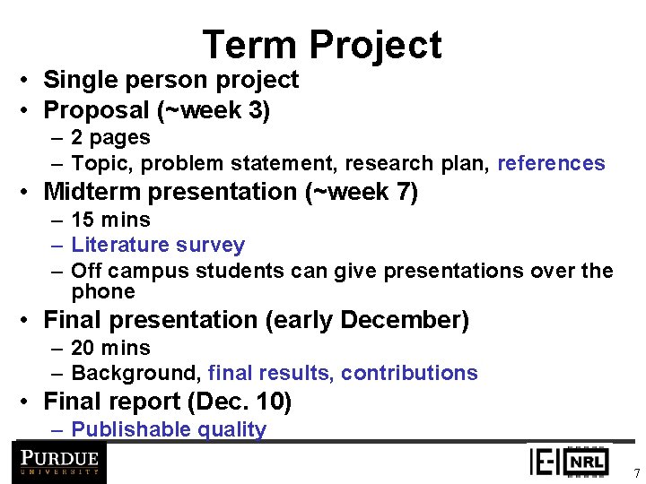
Class Organization • One exam (40% of overall grade) • Term-long project (60%) – Proposal (5%) – Midterm presentation (15%) – background material and proposed work – Final presentation (20%) – Final report (20%) 5
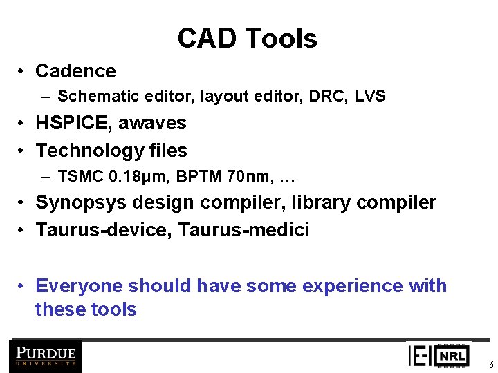
CAD Tools • Cadence – Schematic editor, layout editor, DRC, LVS • HSPICE, awaves • Technology files – TSMC 0. 18μm, BPTM 70 nm, … • Synopsys design compiler, library compiler • Taurus-device, Taurus-medici • Everyone should have some experience with these tools 6
Term Project • Single person project • Proposal (~week 3) – 2 pages – Topic, problem statement, research plan, references • Midterm presentation (~week 7) – 15 mins – Literature survey – Off campus students can give presentations over the phone • Final presentation (early December) – 20 mins – Background, final results, contributions • Final report (Dec. 10) – Publishable quality 7
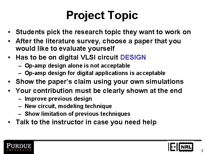
Project Topic • Students pick the research topic they want to work on • After the literature survey, choose a paper that you would like to evaluate yourself • Has to be on digital VLSI circuit DESIGN – Op-amp design alone is not acceptable – Op-amp design for digital applications is acceptable • Show the paper’s claim using your own simulations • Your contribution must be clearly shown at the end – Improve previous design – New circuit, modeling technique – Show limitation of previous techniques • Talk to the instructor in case you need help 8
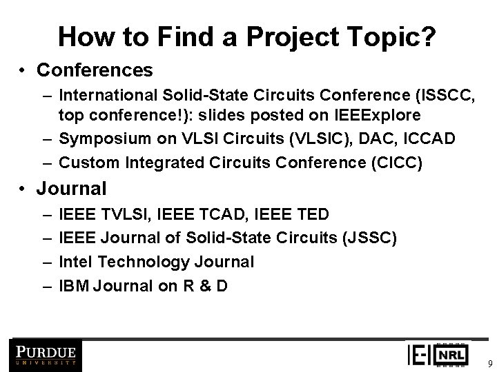
How to Find a Project Topic? • Conferences – International Solid-State Circuits Conference (ISSCC, top conference!): slides posted on IEEExplore – Symposium on VLSI Circuits (VLSIC), DAC, ICCAD – Custom Integrated Circuits Conference (CICC) • Journal – – IEEE TVLSI, IEEE TCAD, IEEE TED IEEE Journal of Solid-State Circuits (JSSC) Intel Technology Journal IBM Journal on R & D 9
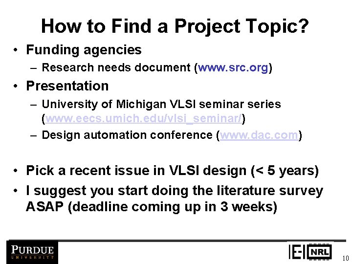
How to Find a Project Topic? • Funding agencies – Research needs document (www. src. org) • Presentation – University of Michigan VLSI seminar series (www. eecs. umich. edu/vlsi_seminar/) – Design automation conference (www. dac. com) • Pick a recent issue in VLSI design (< 5 years) • I suggest you start doing the literature survey ASAP (deadline coming up in 3 weeks) 10
Acknowledgements • Prof. Chris Kim • Intel circuit research labs (S. Borkar and many others) • IBM • Copy right 2002 J. Rabaey et al. 11
Academic Misconduct • Students caught engaging in an academically dishonest practice will receive a failing grade for the course. • University policy on academic dishonesty will be followed strictly. 12
Course Topics • Scaling issues • High performance design – High performance logic family, clocking strategies, interconnects • Low power design – Low voltage designs, leakage control techniques, circuit/device/technology issues, low power SRAM • Variation tolerant design – Process compensating techniques • Power delivery, interconnect, reliability • Bulk and SOI 13
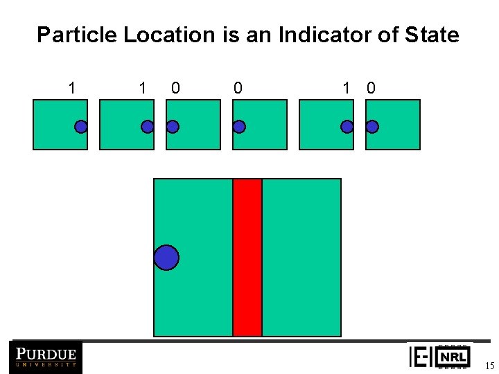
A physical system as a computing medium • We need to create a bit first. Information processing always requires physical carrier, which are material particles. • First requirement to physical realization of a bit implies creating distinguishable states within a system of such material particles. • The second requirement is conditional change of state. • The properties of distinguishability and conditional change of state are two fundamental properties of a material subsystem to represent information. These properties can be obtained by creating energy barriers in a material system. 14
Particle Location is an Indicator of State 1 1 0 0 15
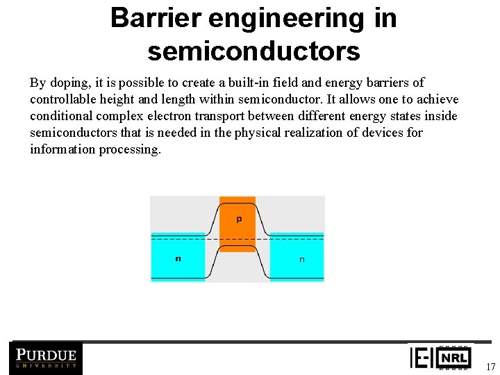
Barrier engineering in semiconductors By doping, it is possible to create a built-in field and energy barriers of controllable height and length within semiconductor. It allows one to achieve conditional complex electron transport between different energy states inside semiconductors that is needed in the physical realization of devices for information processing. 17
Kroemer’s Lemma of Proven Ignorance • If in discussing a semiconductor problem, you cannot draw an Energy. Band-Diagram, this shows that you don’t know what are you talking about • If you can draw one, but don’t, then your audience won’t know what are you talking about 18
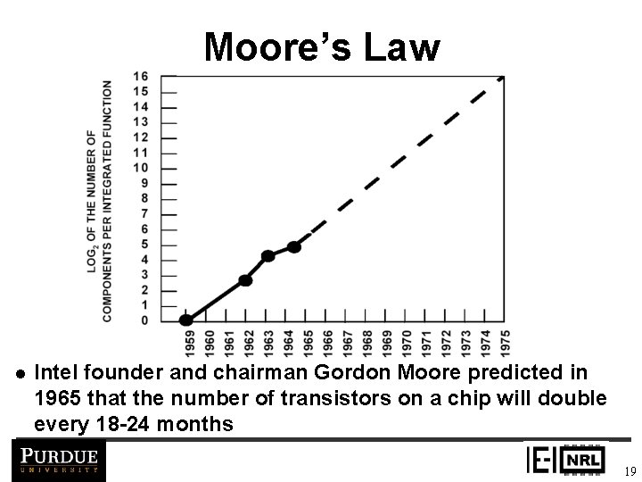
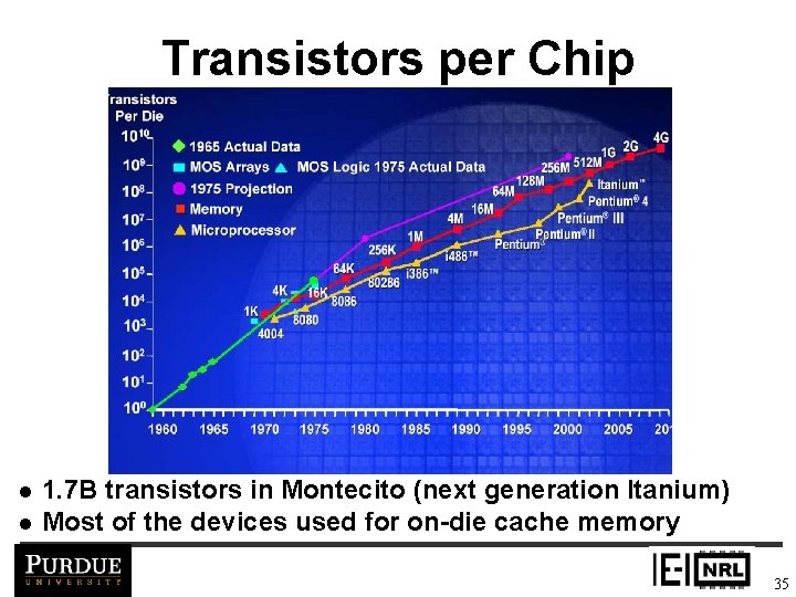
Moore’s Law l Intel founder and chairman Gordon Moore predicted in 1965 that the number of transistors on a chip will double every 18 -24 months 19
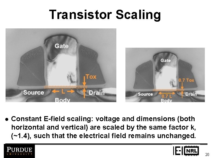
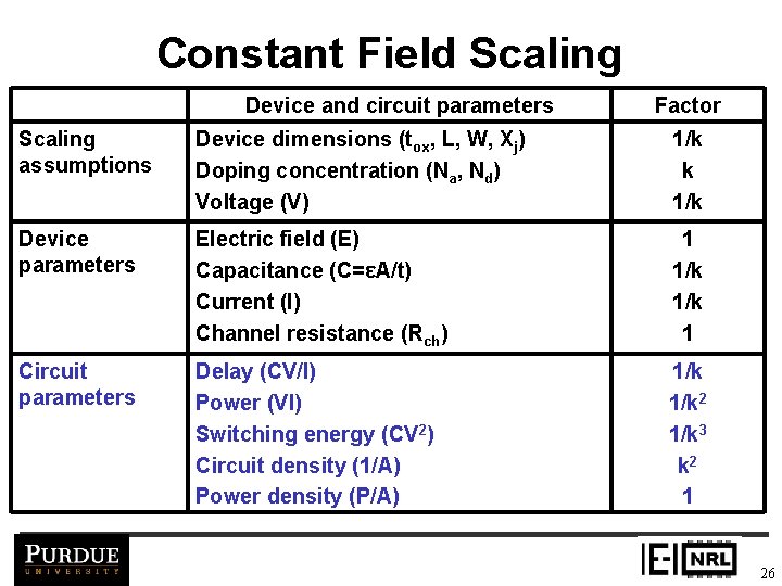
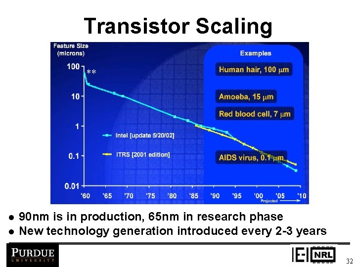
Transistor Scaling l Constant E-field scaling: voltage and dimensions (both horizontal and vertical) are scaled by the same factor k, (~1. 4), such that the electrical field remains unchanged. 20
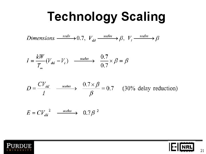
Technology Scaling 21
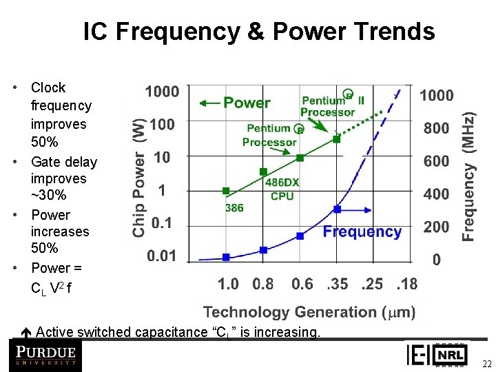
IC Frequency & Power Trends • Clock frequency improves 50% • Gate delay improves ~30% • Power increases 50% • Power = C L V 2 f Active switched capacitance “CL” is increasing. 22
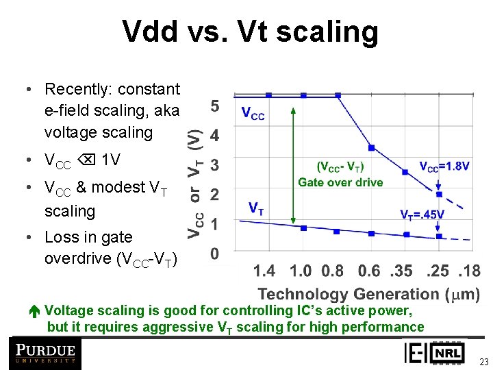
Vdd vs. Vt scaling • Recently: constant e-field scaling, aka voltage scaling • VCC 1 V • VCC & modest VT scaling • Loss in gate overdrive (VCC-VT) Voltage scaling is good for controlling IC’s active power, but it requires aggressive VT scaling for high performance 23
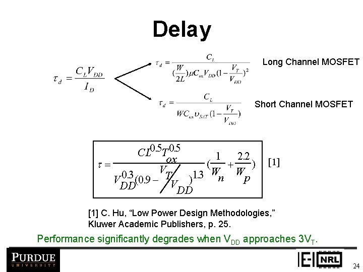
Delay Long Channel MOSFET Short Channel MOSFET . CL 0. 5 T 05 1 2. 2 ox ( ) t= + V W W. n p V 0. 3(0. 9 - TV )13 DD DD [1] C. Hu, “Low Power Design Methodologies, ” Kluwer Academic Publishers, p. 25. Performance significantly degrades when VDD approaches 3 VT. 24
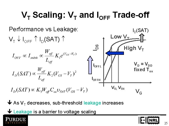
VT Scaling: VT and IOFF Trade-off Performance vs Leakage: Low VT IDS VT IOFF ID(SAT) High VT VD = VDD fixed Tox IOFFL IOFFH VTL VTH VG As VT decreases, sub-threshold leakage increases Leakage is a barrier to voltage scaling 25
Constant Field Scaling Device and circuit parameters Factor Scaling assumptions Device dimensions (tox, L, W, Xj) Doping concentration (Na, Nd) Voltage (V) 1/k k 1/k Device parameters Electric field (E) Capacitance (C=εA/t) Current (I) Channel resistance (Rch) 1 1/k 1 Circuit parameters Delay (CV/I) Power (VI) Switching energy (CV 2) Circuit density (1/A) Power density (P/A) 1/k 2 1/k 3 k 2 1 26
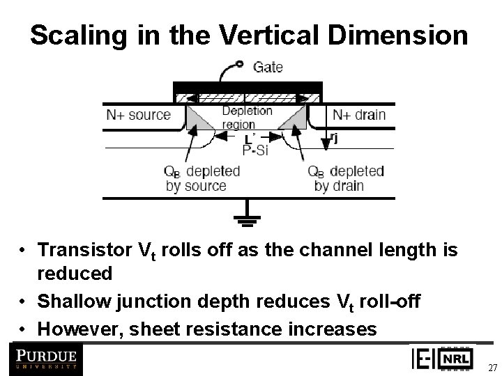
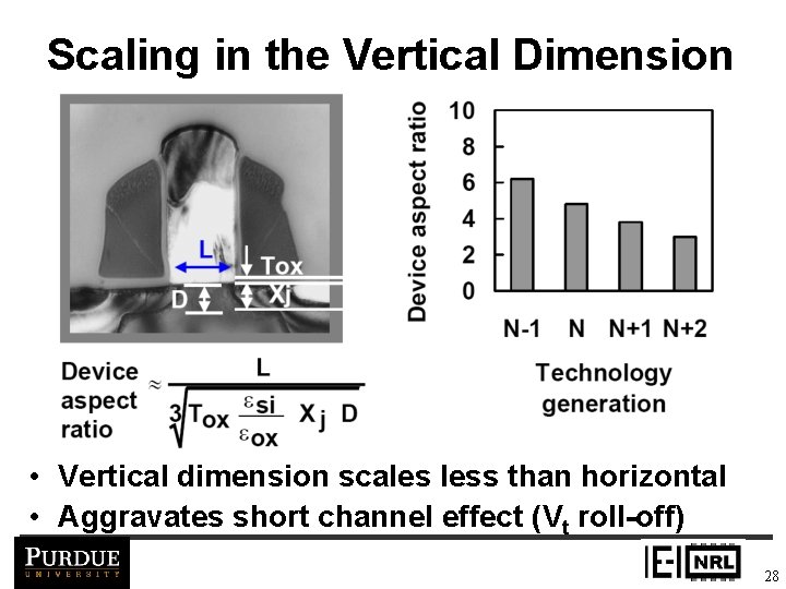
Scaling in the Vertical Dimension • Transistor Vt rolls off as the channel length is reduced • Shallow junction depth reduces Vt roll-off • However, sheet resistance increases 27
Scaling in the Vertical Dimension • Vertical dimension scales less than horizontal • Aggravates short channel effect (Vt roll-off) 28
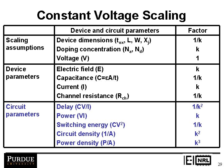
Constant Voltage Scaling Device and circuit parameters Factor Scaling assumptions Device dimensions (tox, L, W, Xj) Doping concentration (Na, Nd) Voltage (V) 1/k k 1 Device parameters Electric field (E) Capacitance (C=εA/t) Current (I) Channel resistance (Rch) k 1/k Circuit parameters Delay (CV/I) Power (VI) Switching energy (CV 2) Circuit density (1/A) Power density (P/A) 1/k 2 k 1/k k 2 k 3 29
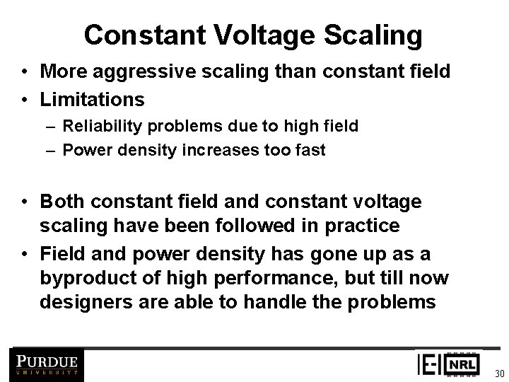
Constant Voltage Scaling • More aggressive scaling than constant field • Limitations – Reliability problems due to high field – Power density increases too fast • Both constant field and constant voltage scaling have been followed in practice • Field and power density has gone up as a byproduct of high performance, but till now designers are able to handle the problems 30
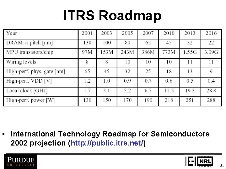
ITRS Roadmap • International Technology Roadmap for Semiconductors 2002 projection (http: //public. itrs. net/) 31
Transistor Scaling l l 90 nm is in production, 65 nm in research phase New technology generation introduced every 2 -3 years 32
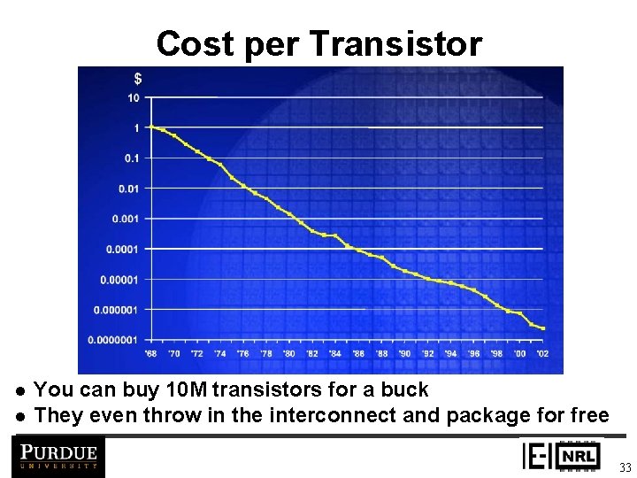
Cost per Transistor l l You can buy 10 M transistors for a buck They even throw in the interconnect and package for free 33
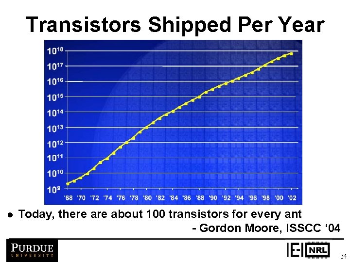
Transistors Shipped Per Year l Today, there about 100 transistors for every ant - Gordon Moore, ISSCC ‘ 04 34
Transistors per Chip l l 1. 7 B transistors in Montecito (next generation Itanium) Most of the devices used for on-die cache memory 35
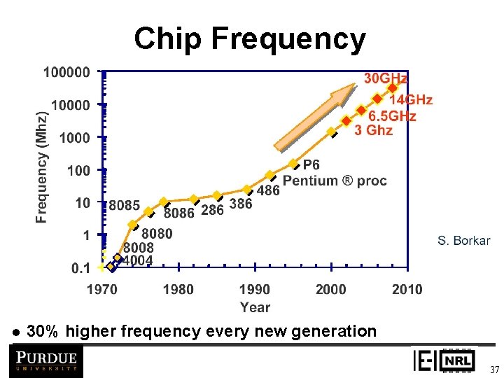
Chip Frequency l 30% higher frequency every new generation 37
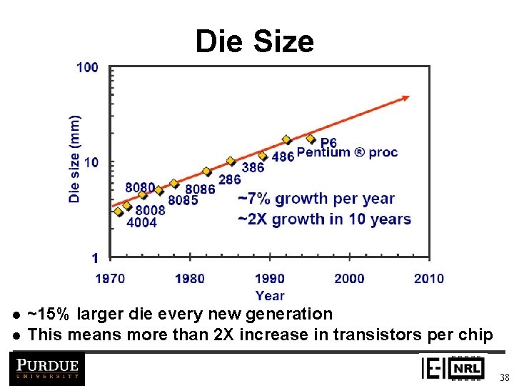
Die Size l l ~15% larger die every new generation This means more than 2 X increase in transistors per chip 38
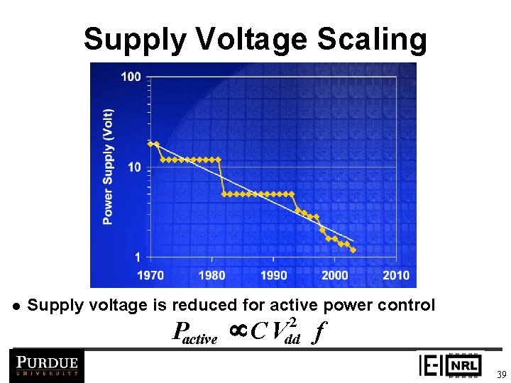
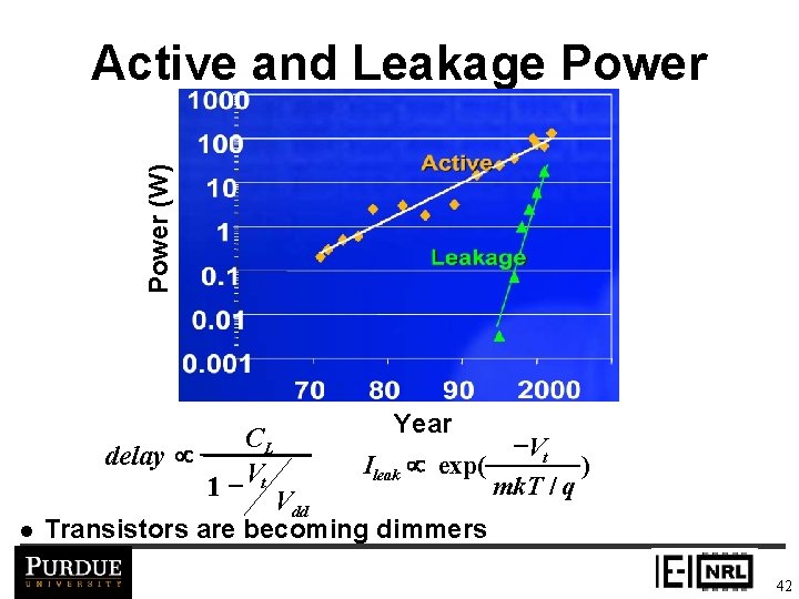
Supply Voltage Scaling l Supply voltage is reduced for active power control Pactive µ C Vdd 2 f 39
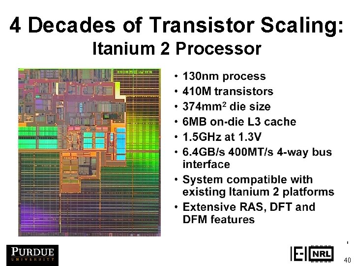
4 Decades of Transistor Scaling: Itanium 2 Processor 40
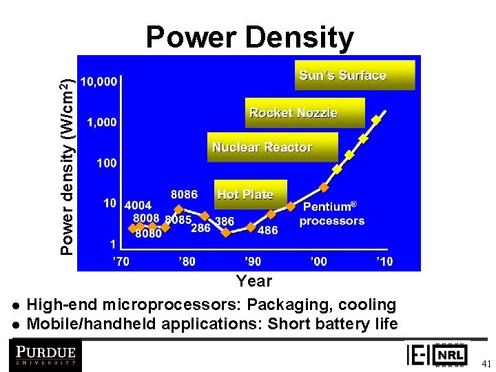
Power density (W/cm 2) Power Density l l Year High-end microprocessors: Packaging, cooling Mobile/handheld applications: Short battery life 41
Power (W) Active and Leakage Power l Year CL -Vt delay µ Ileak µ exp( ) V mk. T / q 1 - t Vdd Transistors are becoming dimmers 42
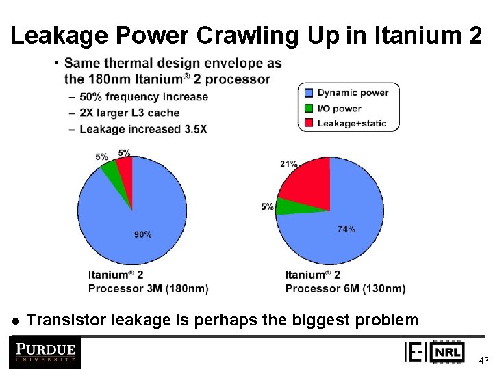
Leakage Power Crawling Up in Itanium 2 l Transistor leakage is perhaps the biggest problem 43
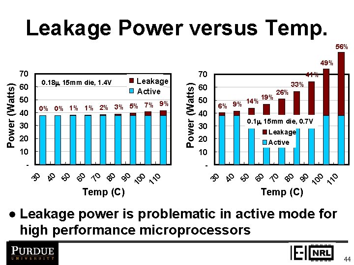
Leakage Power versus Temp. 56% 49% 0. 18 m, 15 mm die, 1. 4 V 30 20 10 50 40 14% 6% 9% 19% 26% 0. 1 m, 15 mm die, 0. 7 V 30 Leakage Active 20 10 0 11 0 10 90 80 70 60 50 Temp (C) l 33% 60 40 30 - 41% 40 40 9% 0% 0% 1% 1% 2% 3% 5% 7% 70 30 60 50 Leakage Active Power (Watts) 70 Temp (C) Leakage power is problematic in active mode for high performance microprocessors 44
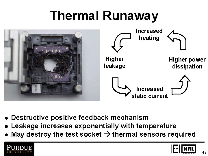
Thermal Runaway Increased heating Higher leakage Higher power dissipation Increased static current l l l Destructive positive feedback mechanism Leakage increases exponentially with temperature May destroy the test socket thermal sensors required 45
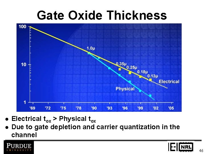
Gate Oxide Thickness l l Electrical tox > Physical tox Due to gate depletion and carrier quantization in the channel 46
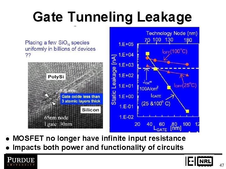
Gate Tunneling Leakage l l MOSFET no longer have infinite input resistance Impacts both power and functionality of circuits 47
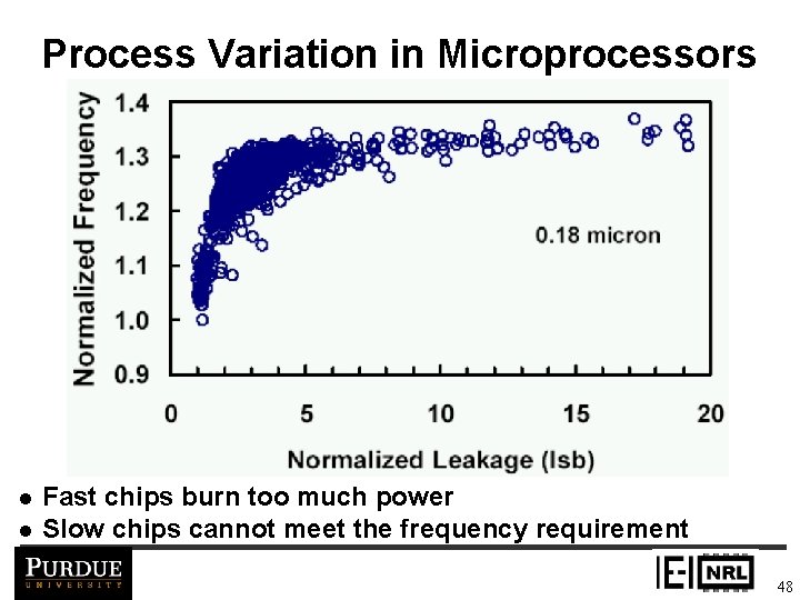
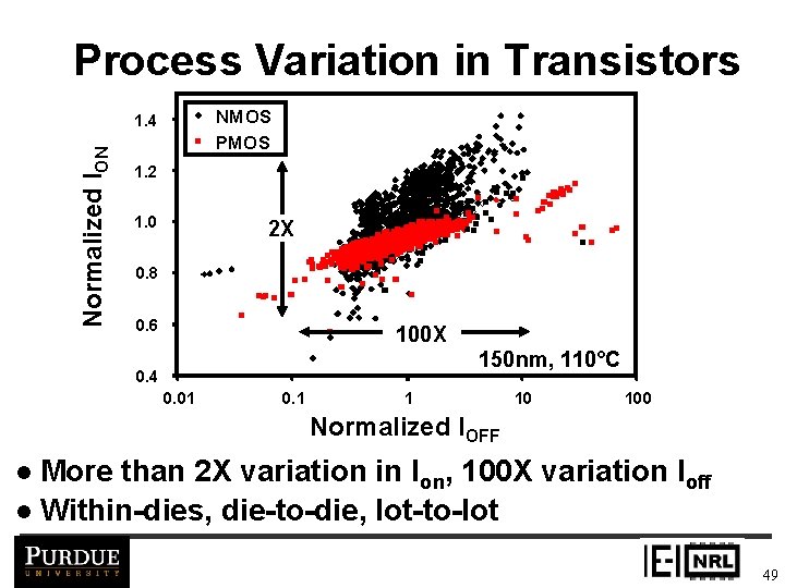
Process Variation in Microprocessors l l Fast chips burn too much power Slow chips cannot meet the frequency requirement 48
Process Variation in Transistors NMOS PMOS Normalized ION 1. 4 1. 2 1. 0 2 X 0. 8 0. 6 100 X 150 nm, 110°C 0. 4 0. 01 0. 1 1 10 100 Normalized IOFF More than 2 X variation in Ion, 100 X variation Ioff l Within-dies, die-to-die, lot-to-lot l 49
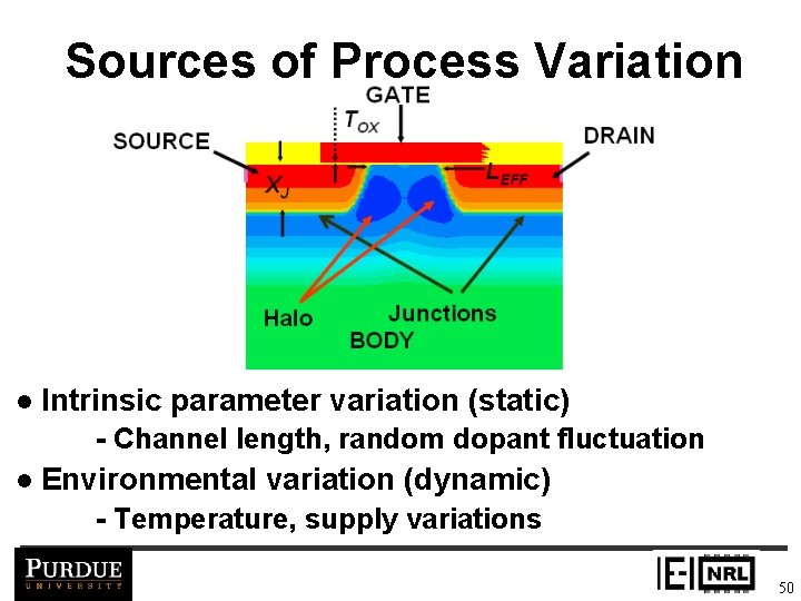
Sources of Process Variation l Intrinsic parameter variation (static) - Channel length, random dopant fluctuation l Environmental variation (dynamic) - Temperature, supply variations 50
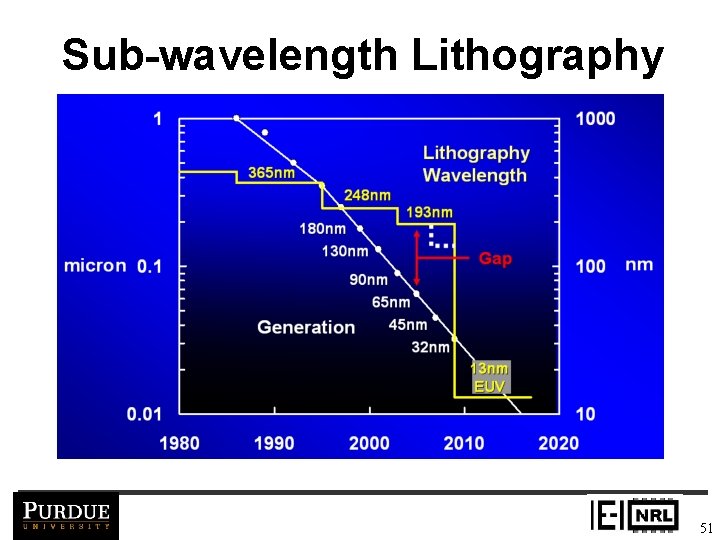
Sub-wavelength Lithography 51
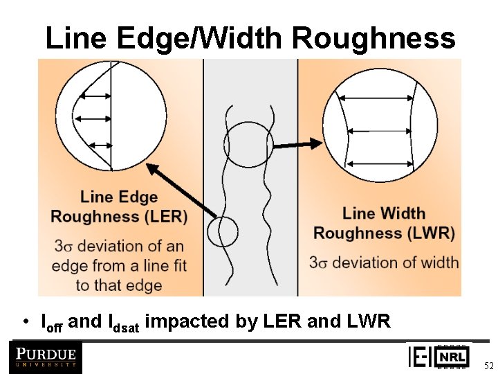
Line Edge/Width Roughness • Ioff and Idsat impacted by LER and LWR 52
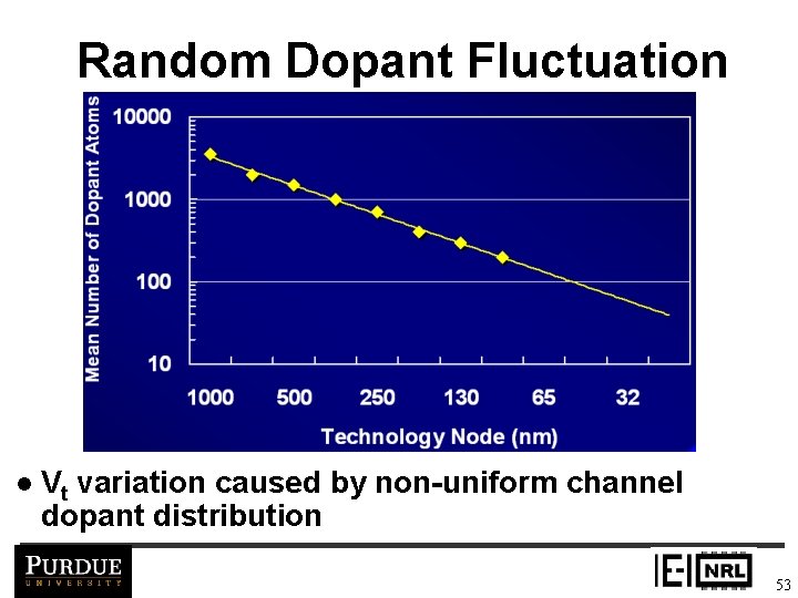
Random Dopant Fluctuation l Vt variation caused by non-uniform channel dopant distribution 53
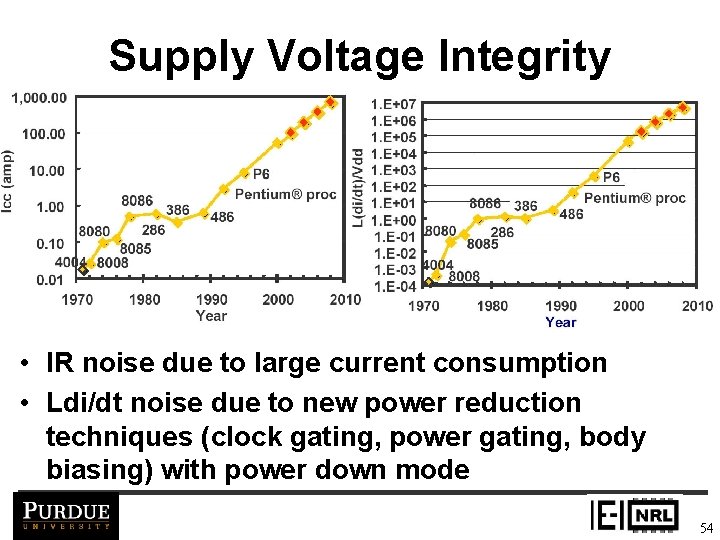
Supply Voltage Integrity • IR noise due to large current consumption • Ldi/dt noise due to new power reduction techniques (clock gating, power gating, body biasing) with power down mode 54
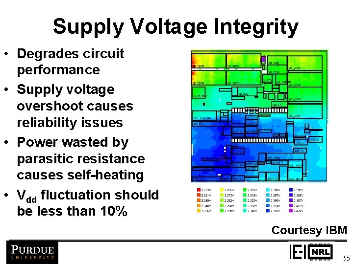
Supply Voltage Integrity • Degrades circuit performance • Supply voltage overshoot causes reliability issues • Power wasted by parasitic resistance causes self-heating • Vdd fluctuation should be less than 10% Courtesy IBM 55
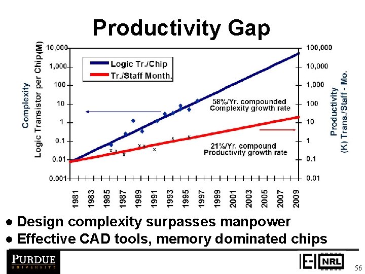
Productivity Gap Design complexity surpasses manpower l Effective CAD tools, memory dominated chips l 56
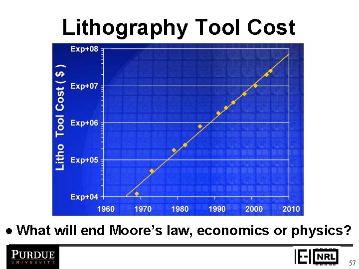
Lithography Tool Cost l What will end Moore’s law, economics or physics? 57
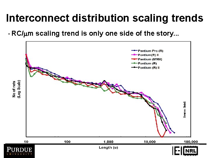
Interconnect Scaling • Global interconnects get longer due to larger die size • Wire scaling increases R, L and C • Example: local vs. global interconnect delay 58
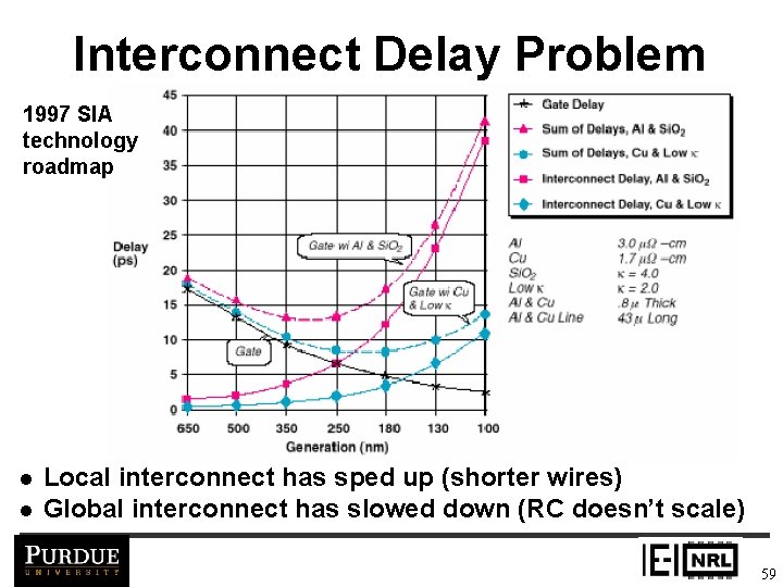
Interconnect Delay Problem 1997 SIA technology roadmap l l Local interconnect has sped up (shorter wires) Global interconnect has slowed down (RC doesn’t scale) 59
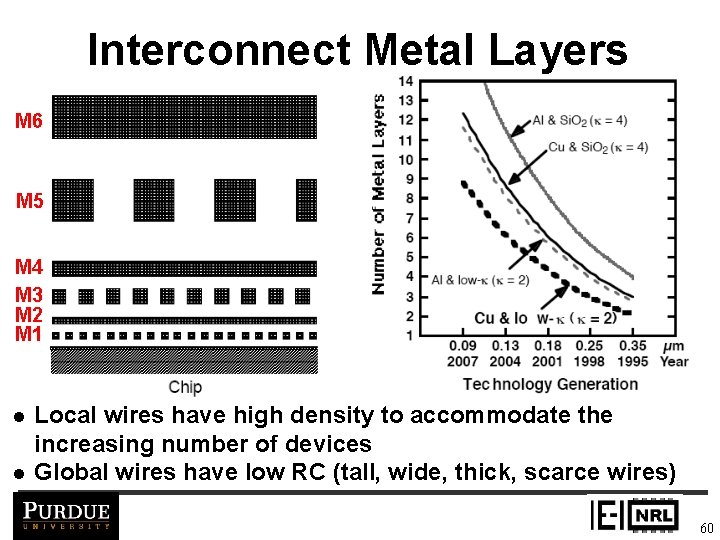
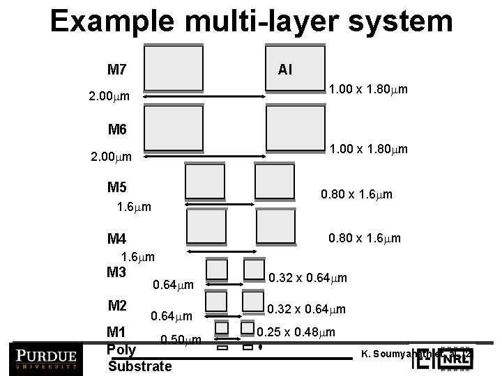
Interconnect Metal Layers M 6 M 5 M 4 M 3 M 2 M 1 l l Local wires have high density to accommodate the increasing number of devices Global wires have low RC (tall, wide, thick, scarce wires) 60
Interconnect distribution scaling trends scaling trend is only one side of the story. . . Source: Intel • RC/mm
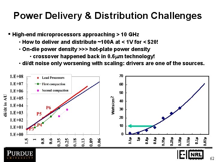
Power Delivery & Distribution Challenges • High-end microprocessors approaching > 10 GHz • How to deliver and distribute ~100 A at < 1 V for < $20! • On-die power density >>> hot-plate power density • crossover happened back in 0. 6 mm technology! • di/dt noise only worsening with scaling: drivers are one of the sources. 70 60 Watts/cm 2 50 40 30 20 10 0 62
Example multi-layer system M 7 Al 1. 00 x 1. 80 mm 2. 00 mm M 6 1. 00 x 1. 80 mm 2. 00 mm M 5 0. 80 x 1. 6 mm M 4 1. 6 mm M 3 M 2 0. 64 mm M 1 0. 50 mm Poly Substrate 0. 32 x 0. 64 mm 0. 25 x 0. 48 mm K. Soumyanath et. al. [2]
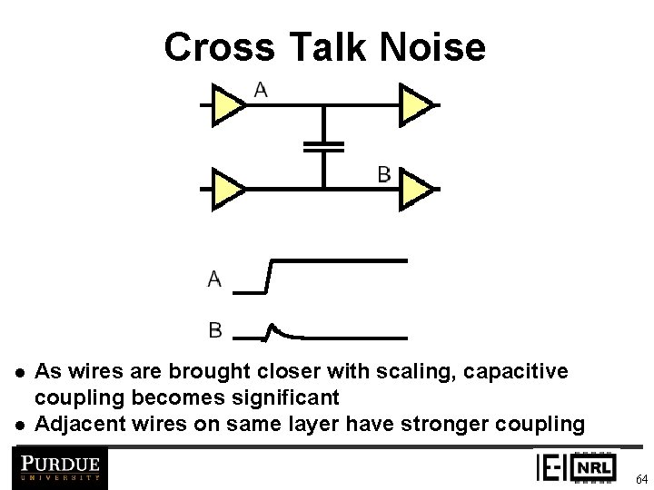
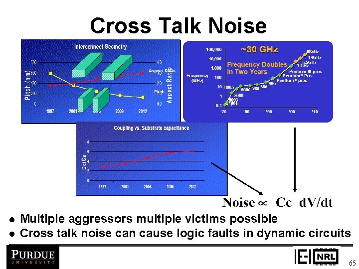
Cross Talk Noise l l As wires are brought closer with scaling, capacitive coupling becomes significant Adjacent wires on same layer have stronger coupling 64
Cross Talk Noise l l Multiple aggressors multiple victims possible Cross talk noise can cause logic faults in dynamic circuits 65
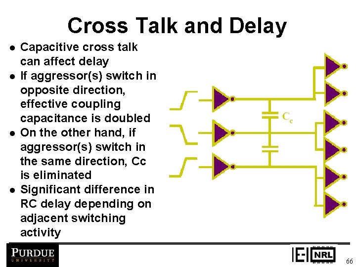
Cross Talk and Delay l l Capacitive cross talk can affect delay If aggressor(s) switch in opposite direction, effective coupling capacitance is doubled On the other hand, if aggressor(s) switch in the same direction, Cc is eliminated Significant difference in RC delay depending on adjacent switching activity 66
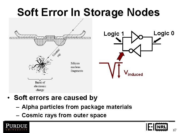
Soft Error In Storage Nodes Logic 1 Logic 0 Vinduced • Soft errors are caused by – Alpha particles from package materials – Cosmic rays from outer space 67
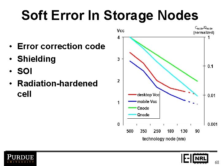
Soft Error In Storage Nodes • • Error correction code Shielding SOI Radiation-hardened cell 68
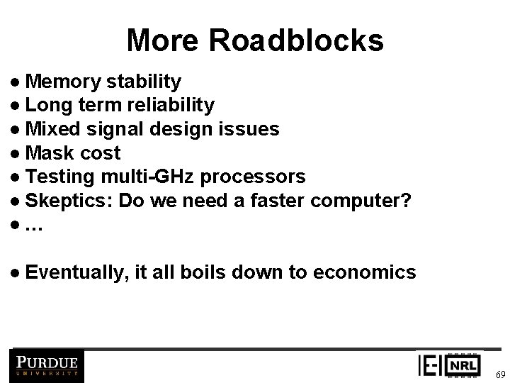
More Roadblocks Memory stability l Long term reliability l Mixed signal design issues l Mask cost l Testing multi-GHz processors l Skeptics: Do we need a faster computer? l… l l Eventually, it all boils down to economics 69
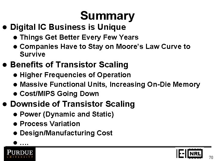
Summary l Digital IC Business is Unique Things Get Better Every Few Years l Companies Have to Stay on Moore’s Law Curve to Survive l l Benefits of Transistor Scaling Higher Frequencies of Operation l Massive Functional Units, Increasing On-Die Memory l Cost/MIPS Going Down l l Downside of Transistor Scaling Power (Dynamic and Static) l Process Variation l Design/Manufacturing Cost l …. l 70