EE 4800 CMOS Digital IC Design Analysis Lecture
- Slides: 42

EE 4800 CMOS Digital IC Design & Analysis Lecture 3 MOS Transistor Device Characteristics Zhuo Feng 3. 1 Z. Feng MTU EE 4800 CMOS Digital IC Design & Analysis

Outline ■ ■ ■ ■ 3. 2 Introduction MOS Capacitor NMOS I-V Characteristics PMOS I-V Characteristics Gate and Diffusion Capacitance Nonideal Transistor Behavior Process and Environmental Variations Z. Feng MTU EE 4800 CMOS Digital IC Design & Analysis

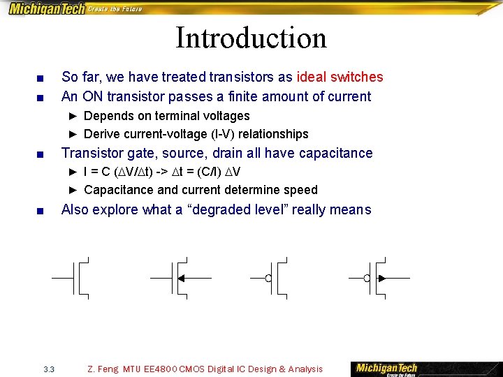
Introduction ■ ■ So far, we have treated transistors as ideal switches An ON transistor passes a finite amount of current ► Depends on terminal voltages ► Derive current-voltage (I-V) relationships ■ Transistor gate, source, drain all have capacitance ► I = C (DV/Dt) -> Dt = (C/I) DV ► Capacitance and current determine speed ■ 3. 3 Also explore what a “degraded level” really means Z. Feng MTU EE 4800 CMOS Digital IC Design & Analysis

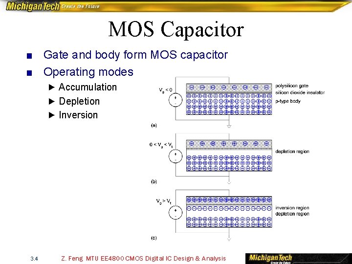
MOS Capacitor ■ Gate and body form MOS capacitor ■ Operating modes ► Accumulation ► Depletion ► Inversion 3. 4 Z. Feng MTU EE 4800 CMOS Digital IC Design & Analysis

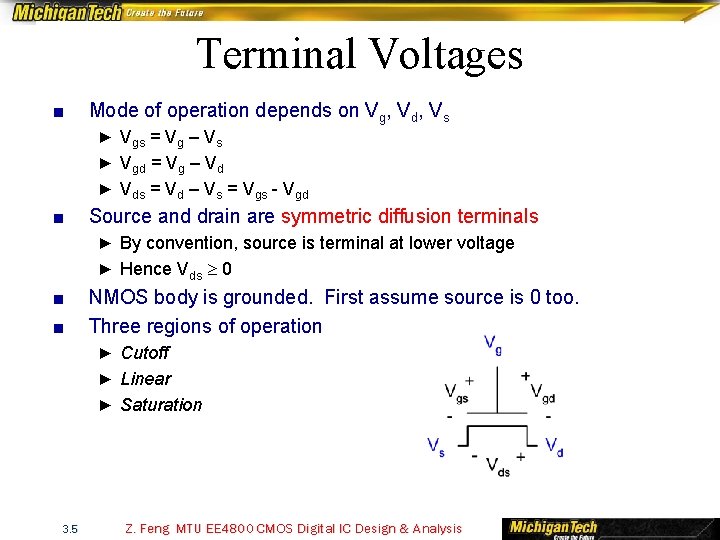
Terminal Voltages ■ Mode of operation depends on Vg, Vd, Vs ► Vgs = Vg – Vs ► Vgd = Vg – Vd ► Vds = Vd – Vs = Vgs - Vgd ■ Source and drain are symmetric diffusion terminals ► By convention, source is terminal at lower voltage ► Hence Vds 0 ■ ■ NMOS body is grounded. First assume source is 0 too. Three regions of operation ► Cutoff ► Linear ► Saturation 3. 5 Z. Feng MTU EE 4800 CMOS Digital IC Design & Analysis

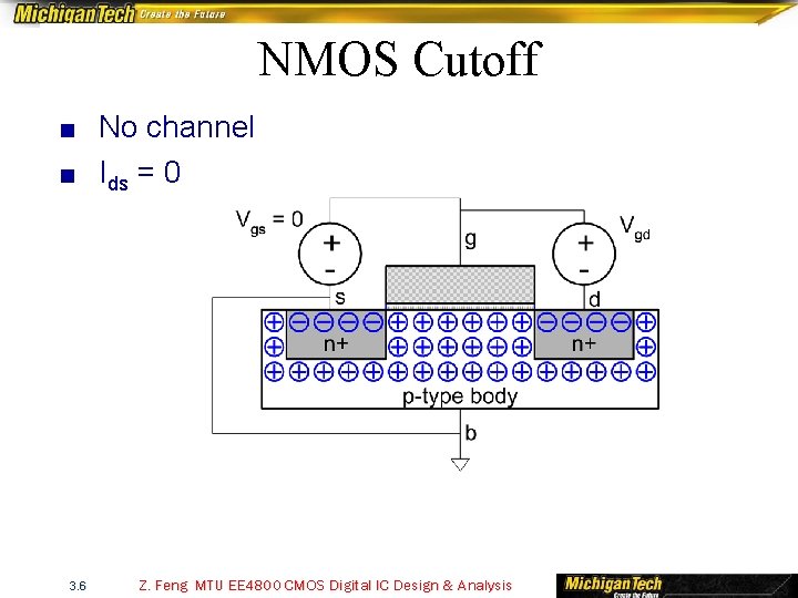
NMOS Cutoff ■ No channel ■ Ids = 0 3. 6 Z. Feng MTU EE 4800 CMOS Digital IC Design & Analysis

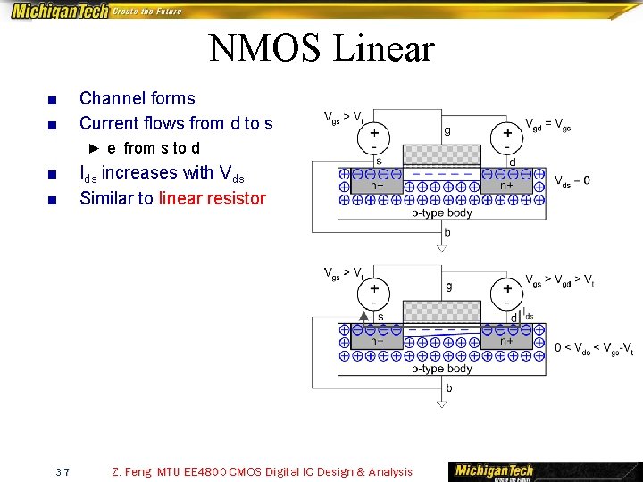
NMOS Linear ■ ■ Channel forms Current flows from d to s ► e- from s to d ■ ■ 3. 7 Ids increases with Vds Similar to linear resistor Z. Feng MTU EE 4800 CMOS Digital IC Design & Analysis

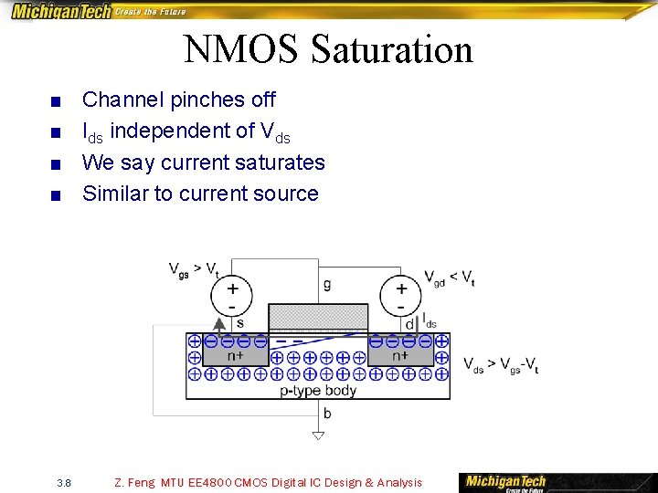
NMOS Saturation ■ ■ 3. 8 Channel pinches off Ids independent of Vds We say current saturates Similar to current source Z. Feng MTU EE 4800 CMOS Digital IC Design & Analysis

I-V Characteristics ■ In Linear region, Ids depends on ► How much charge is in the channel? ► How fast is the charge moving? 3. 9 Z. Feng MTU EE 4800 CMOS Digital IC Design & Analysis

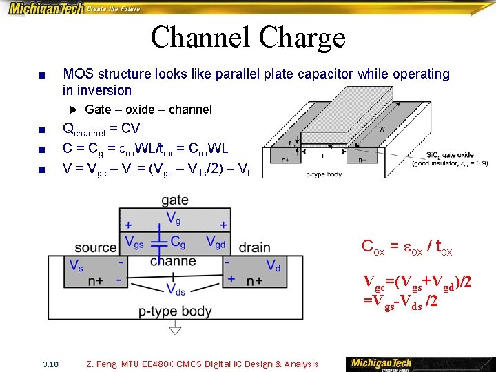
Channel Charge ■ MOS structure looks like parallel plate capacitor while operating in inversion ► Gate – oxide – channel ■ ■ ■ Qchannel = CV C = Cg = eox. WL/tox = Cox. WL V = Vgc – Vt = (Vgs – Vds/2) – Vt Cox = eox / tox Vgc=(Vgs+Vgd)/2 =Vgs-Vds /2 3. 10 Z. Feng MTU EE 4800 CMOS Digital IC Design & Analysis

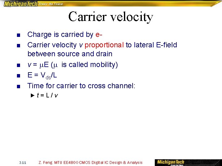
Carrier velocity ■ Charge is carried by e■ Carrier velocity v proportional to lateral E-field between source and drain ■ v = m. E (m is called mobility) ■ E = Vds/L ■ Time for carrier to cross channel: ►t=L/v 3. 11 Z. Feng MTU EE 4800 CMOS Digital IC Design & Analysis

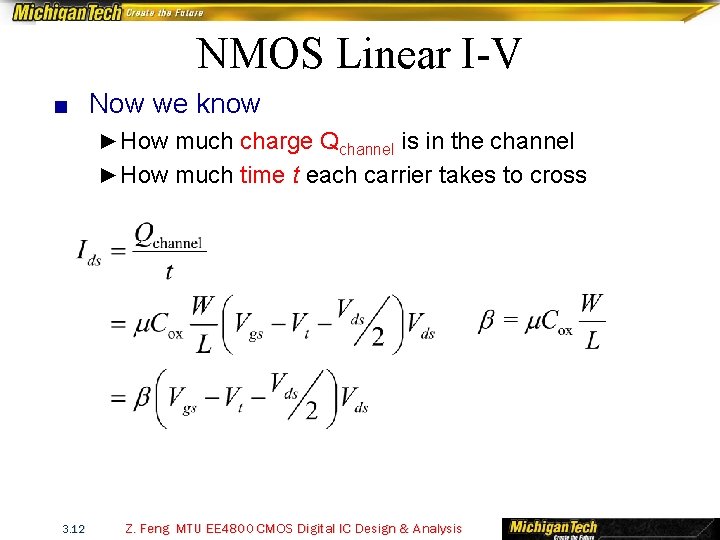
NMOS Linear I-V ■ Now we know ► How much charge Qchannel is in the channel ► How much time t each carrier takes to cross 3. 12 Z. Feng MTU EE 4800 CMOS Digital IC Design & Analysis

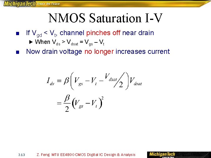
NMOS Saturation I-V ■ If Vgd < Vt, channel pinches off near drain ► When Vds > Vdsat = Vgs – Vt ■ Now drain voltage no longer increases current 3. 13 Z. Feng MTU EE 4800 CMOS Digital IC Design & Analysis

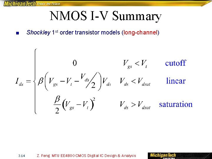
NMOS I-V Summary ■ 3. 14 Shockley 1 st order transistor models (long-channel) Z. Feng MTU EE 4800 CMOS Digital IC Design & Analysis

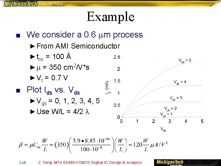
Example ■ We consider a 0. 6 mm process ► From AMI Semiconductor ► tox = 100 Å ► m = 350 cm 2/V*s ► Vt = 0. 7 V ■ Plot Ids vs. Vds ► Vgs = 0, 1, 2, 3, 4, 5 ► Use W/L = 4/2 l 3. 15 Z. Feng MTU EE 4800 CMOS Digital IC Design & Analysis

PMOS I-V ■ All dopings and voltages are inverted for PMOS ■ Mobility mp is determined by holes ► Typically 2 -3 x lower than that of electrons mn ► 120 cm 2/V*s in AMI 0. 6 mm process ■ Thus PMOS must be wider to provide same current ► In this class, assume mn / mp = 2 ► *** plot I-V here 3. 16 Z. Feng MTU EE 4800 CMOS Digital IC Design & Analysis

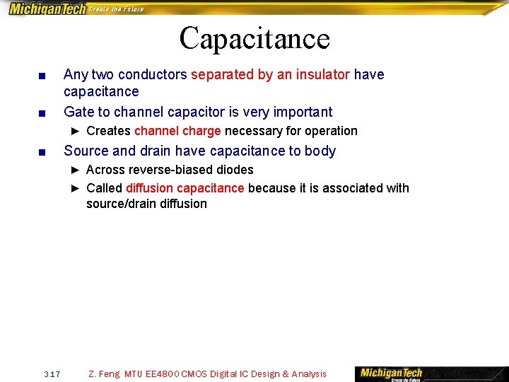
Capacitance ■ ■ Any two conductors separated by an insulator have capacitance Gate to channel capacitor is very important ► Creates channel charge necessary for operation ■ Source and drain have capacitance to body ► Across reverse-biased diodes ► Called diffusion capacitance because it is associated with source/drain diffusion 3. 17 Z. Feng MTU EE 4800 CMOS Digital IC Design & Analysis

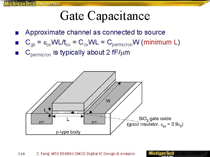
Gate Capacitance ■ Approximate channel as connected to source ■ Cgs = eox. WL/tox = Cox. WL = Cpermicron. W (minimum L) ■ Cpermicron is typically about 2 f. F/mm 3. 18 Z. Feng MTU EE 4800 CMOS Digital IC Design & Analysis

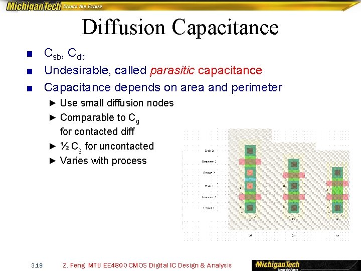
Diffusion Capacitance ■ Csb, Cdb ■ Undesirable, called parasitic capacitance ■ Capacitance depends on area and perimeter ► Use small diffusion nodes ► Comparable to Cg for contacted diff ► ½ Cg for uncontacted ► Varies with process 3. 19 Z. Feng MTU EE 4800 CMOS Digital IC Design & Analysis

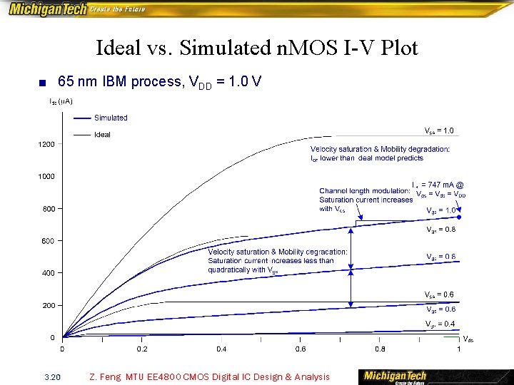
Ideal vs. Simulated n. MOS I-V Plot ■ 65 nm IBM process, VDD = 1. 0 V 3. 20 Z. Feng MTU EE 4800 CMOS Digital IC Design & Analysis

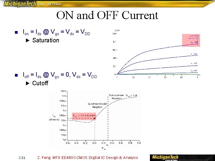
ON and OFF Current ■ Ion = Ids @ Vgs = Vds = VDD ► Saturation ■ Ioff = Ids @ Vgs = 0, Vds = VDD ► Cutoff 3. 21 Z. Feng MTU EE 4800 CMOS Digital IC Design & Analysis

Electric Fields Effects ■ Vertical electric field: Evert = Vgs / tox ► Attracts carriers into channel ► Long channel: Qchannel Evert ■ Lateral electric field: Elat = Vds / L ► Accelerates carriers from drain to source ► Long channel: v = m. Elat 3. 22 Z. Feng MTU EE 4800 CMOS Digital IC Design & Analysis

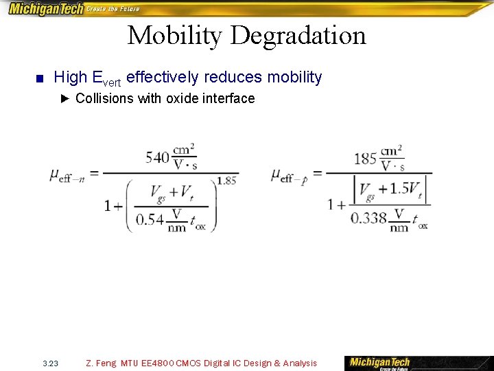
Mobility Degradation ■ High Evert effectively reduces mobility ► Collisions with oxide interface 3. 23 Z. Feng MTU EE 4800 CMOS Digital IC Design & Analysis

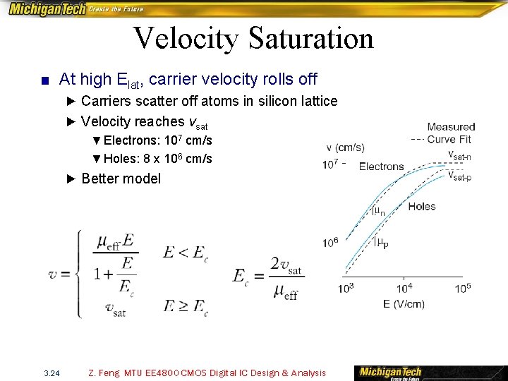
Velocity Saturation ■ At high Elat, carrier velocity rolls off ► Carriers scatter off atoms in silicon lattice ► Velocity reaches vsat ▼ Electrons: 107 cm/s ▼ Holes: 8 x 106 cm/s ► Better model 3. 24 Z. Feng MTU EE 4800 CMOS Digital IC Design & Analysis

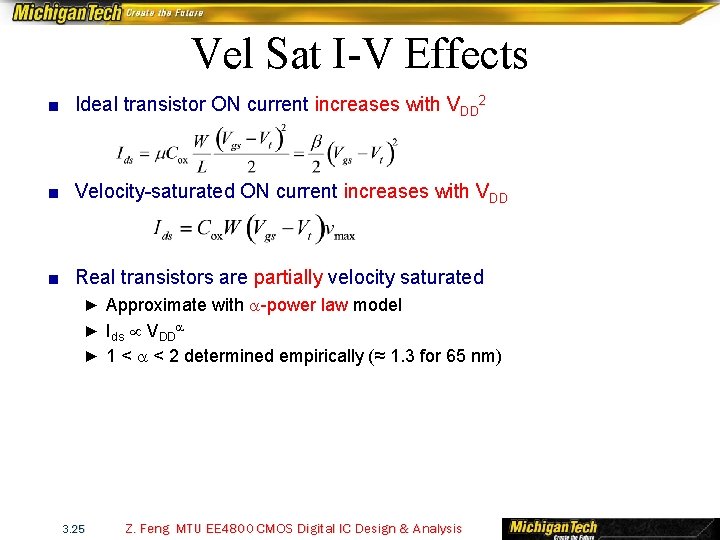
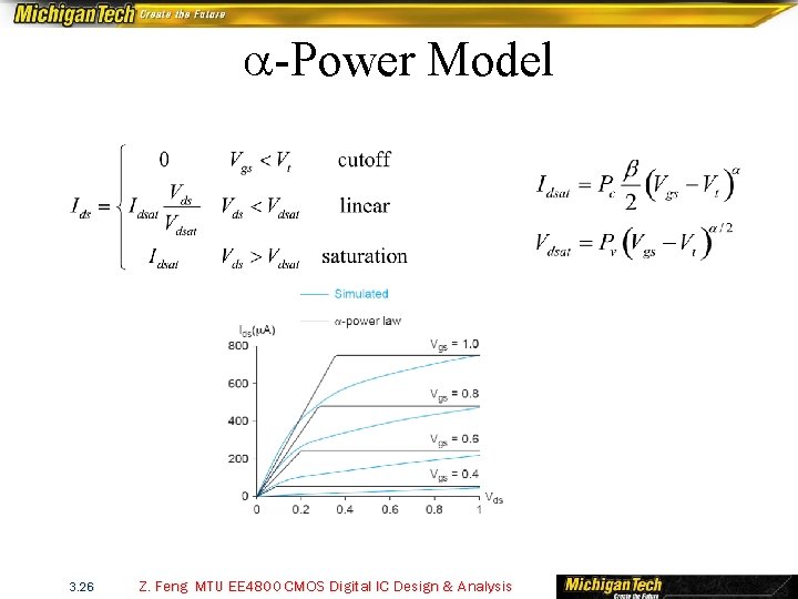
Vel Sat I-V Effects ■ Ideal transistor ON current increases with VDD 2 ■ Velocity-saturated ON current increases with VDD ■ Real transistors are partially velocity saturated ► Approximate with a-power law model ► Ids VDDa ► 1 < a < 2 determined empirically (≈ 1. 3 for 65 nm) 3. 25 Z. Feng MTU EE 4800 CMOS Digital IC Design & Analysis

a-Power Model 3. 26 Z. Feng MTU EE 4800 CMOS Digital IC Design & Analysis

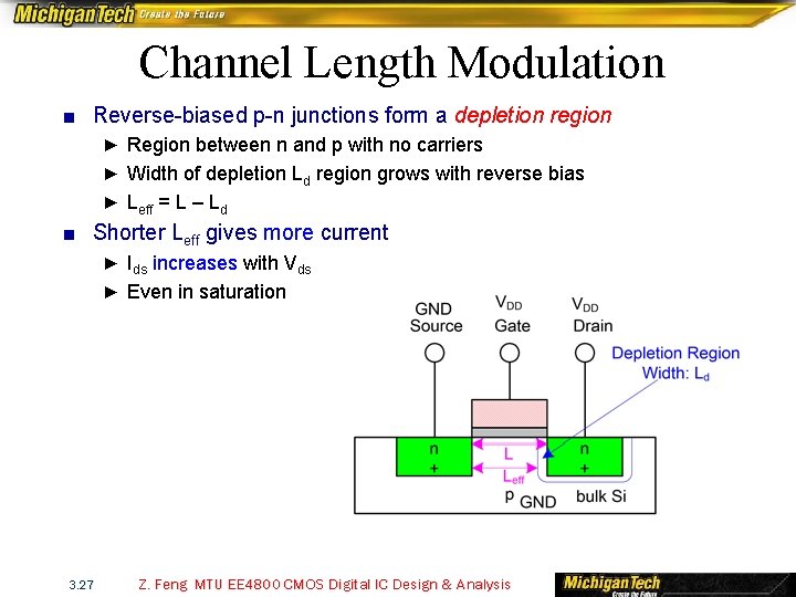
Channel Length Modulation ■ Reverse-biased p-n junctions form a depletion region ► Region between n and p with no carriers ► Width of depletion Ld region grows with reverse bias ► Leff = L – Ld ■ Shorter Leff gives more current ► Ids increases with Vds ► Even in saturation 3. 27 Z. Feng MTU EE 4800 CMOS Digital IC Design & Analysis

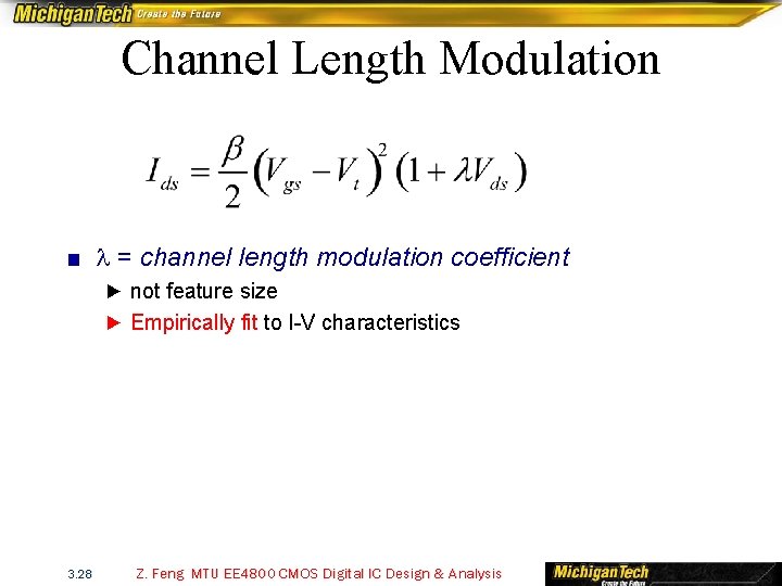
Channel Length Modulation ■ l = channel length modulation coefficient ► not feature size ► Empirically fit to I-V characteristics 3. 28 Z. Feng MTU EE 4800 CMOS Digital IC Design & Analysis

Threshold Voltage Effects ■ Vt is Vgs for which the channel starts to invert ■ Ideal models assumed Vt is constant ■ Really depends (weakly) on almost everything else: ► Body voltage: Body Effect ► Drain voltage: Drain-Induced Barrier Lowering ► Channel length: Short Channel Effect 3. 29 Z. Feng MTU EE 4800 CMOS Digital IC Design & Analysis

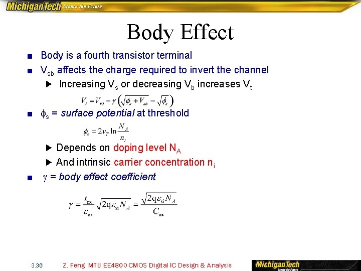
Body Effect ■ Body is a fourth transistor terminal ■ Vsb affects the charge required to invert the channel ► Increasing Vs or decreasing Vb increases Vt ■ fs = surface potential at threshold ► Depends on doping level NA ► And intrinsic carrier concentration ni ■ 3. 30 g = body effect coefficient Z. Feng MTU EE 4800 CMOS Digital IC Design & Analysis

Short Channel Effect ■ In small transistors, source/drain depletion regions extend into the channel ► Impacts the amount of charge required to invert the channel ► And thus makes Vt a function of channel length ■ Short channel effect: Vt increases with L ► Some processes exhibit a reverse short channel effect in which Vt decreases with L 3. 31 Z. Feng MTU EE 4800 CMOS Digital IC Design & Analysis

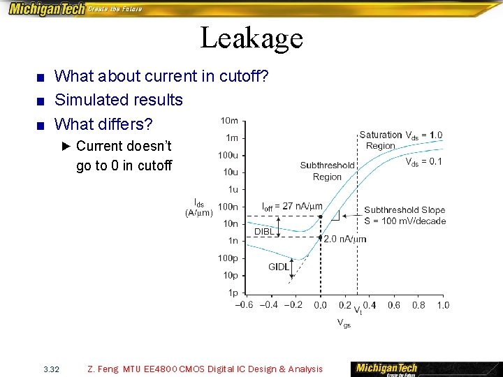
Leakage ■ What about current in cutoff? ■ Simulated results ■ What differs? ► Current doesn’t go to 0 in cutoff 3. 32 Z. Feng MTU EE 4800 CMOS Digital IC Design & Analysis

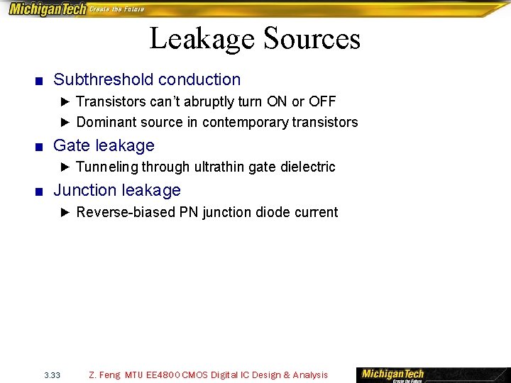
Leakage Sources ■ Subthreshold conduction ► Transistors can’t abruptly turn ON or OFF ► Dominant source in contemporary transistors ■ Gate leakage ► Tunneling through ultrathin gate dielectric ■ Junction leakage ► Reverse-biased PN junction diode current 3. 33 Z. Feng MTU EE 4800 CMOS Digital IC Design & Analysis

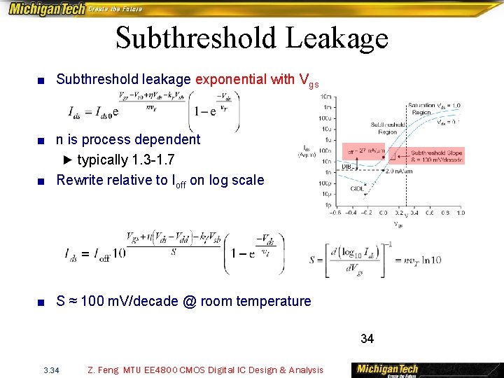
Subthreshold Leakage ■ Subthreshold leakage exponential with Vgs ■ n is process dependent ► typically 1. 3 -1. 7 ■ Rewrite relative to Ioff on log scale ■ S ≈ 100 m. V/decade @ room temperature 34 3. 34 Z. Feng MTU EE 4800 CMOS Digital IC Design & Analysis

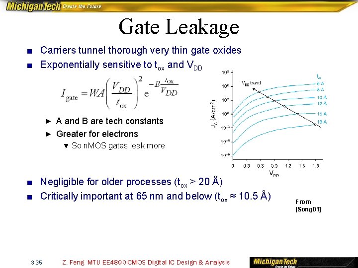
Gate Leakage ■ Carriers tunnel thorough very thin gate oxides ■ Exponentially sensitive to tox and VDD ► A and B are tech constants ► Greater for electrons ▼ So n. MOS gates leak more ■ Negligible for older processes (tox > 20 Å) ■ Critically important at 65 nm and below (tox ≈ 10. 5 Å) 3. 35 Z. Feng MTU EE 4800 CMOS Digital IC Design & Analysis From [Song 01]

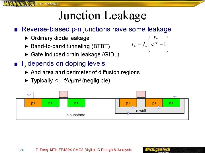
Junction Leakage ■ Reverse-biased p-n junctions have some leakage ► Ordinary diode leakage ► Band-to-band tunneling (BTBT) ► Gate-induced drain leakage (GIDL) ■ Is depends on doping levels ► And area and perimeter of diffusion regions ► Typically < 1 f. A/mm 2 (negligible) 3. 36 Z. Feng MTU EE 4800 CMOS Digital IC Design & Analysis

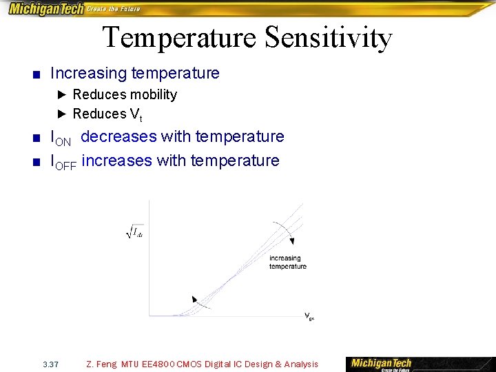
Temperature Sensitivity ■ Increasing temperature ► Reduces mobility ► Reduces Vt ■ ION decreases with temperature ■ IOFF increases with temperature 3. 37 Z. Feng MTU EE 4800 CMOS Digital IC Design & Analysis

So What? ■ So what if transistors are not ideal? ► They still behave like switches. ■ But these effects matter for… ► Supply voltage choice ► Logical effort ► Quiescent power consumption ► Pass transistors ► Temperature of operation 3. 38 Z. Feng MTU EE 4800 CMOS Digital IC Design & Analysis

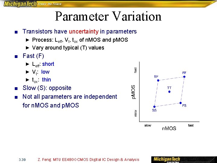
Parameter Variation ■ Transistors have uncertainty in parameters ► Process: Leff, Vt, tox of n. MOS and p. MOS ► Vary around typical (T) values ■ Fast (F) ► Leff: short ► Vt: low ► tox: thin ■ Slow (S): opposite ■ Not all parameters are independent for n. MOS and p. MOS 3. 39 Z. Feng MTU EE 4800 CMOS Digital IC Design & Analysis

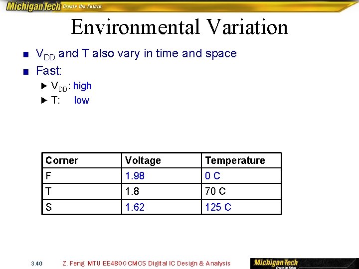
Environmental Variation ■ VDD and T also vary in time and space ■ Fast: ► VDD: high ► T: 3. 40 low Corner Voltage Temperature F 1. 98 0 C T 1. 8 70 C S 1. 62 125 C Z. Feng MTU EE 4800 CMOS Digital IC Design & Analysis

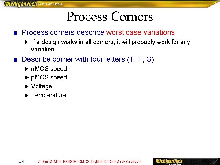
Process Corners ■ Process corners describe worst case variations ► If a design works in all corners, it will probably work for any variation. ■ Describe corner with four letters (T, F, S) ► n. MOS speed ► p. MOS speed ► Voltage ► Temperature 3. 41 Z. Feng MTU EE 4800 CMOS Digital IC Design & Analysis

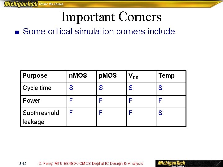
Important Corners ■ Some critical simulation corners include Purpose n. MOS p. MOS VDD Temp Cycle time S S Power F F Subthreshold leakage F F F S 3. 42 Z. Feng MTU EE 4800 CMOS Digital IC Design & Analysis