Introduction to CMOS VLSI Design CMOS Transistor Theory
- Slides: 40

Introduction to CMOS VLSI Design CMOS Transistor Theory MOS devices 1

Outline q q q q Introduction MOS Capacitor n. MOS I-V Characteristics p. MOS I-V Characteristics Gate and Diffusion Capacitance Pass Transistors RC Delay Models MOS devices CMOS VLSI Design 2

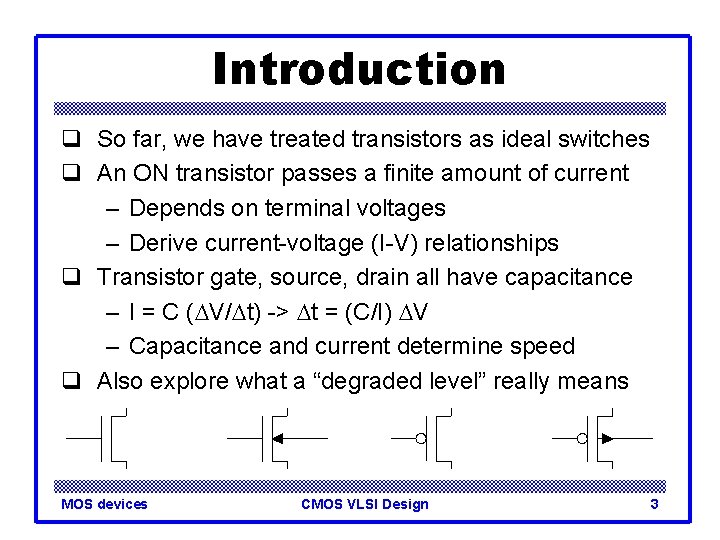
Introduction q So far, we have treated transistors as ideal switches q An ON transistor passes a finite amount of current – Depends on terminal voltages – Derive current-voltage (I-V) relationships q Transistor gate, source, drain all have capacitance – I = C (DV/Dt) -> Dt = (C/I) DV – Capacitance and current determine speed q Also explore what a “degraded level” really means MOS devices CMOS VLSI Design 3

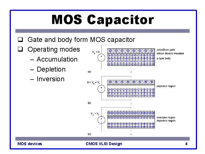
MOS Capacitor q Gate and body form MOS capacitor q Operating modes – Accumulation – Depletion – Inversion MOS devices CMOS VLSI Design 4

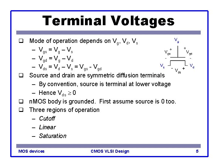
Terminal Voltages q Mode of operation depends on Vg, Vd, Vs – Vgs = Vg – Vs – Vgd = Vg – Vds = Vd – Vs = Vgs - Vgd q Source and drain are symmetric diffusion terminals – By convention, source is terminal at lower voltage – Hence Vds 0 q n. MOS body is grounded. First assume source is 0 too. q Three regions of operation – Cutoff – Linear – Saturation MOS devices CMOS VLSI Design 5

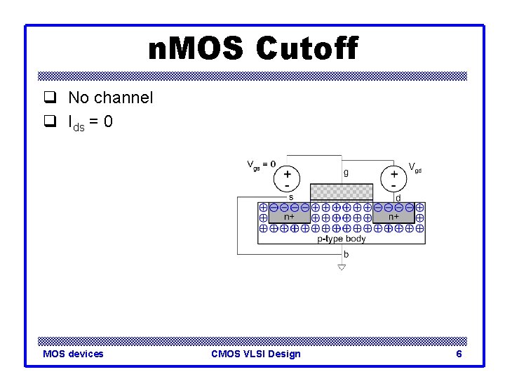
n. MOS Cutoff q No channel q Ids = 0 MOS devices CMOS VLSI Design 6

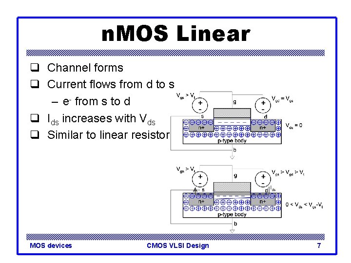
n. MOS Linear q Channel forms q Current flows from d to s – e- from s to d q Ids increases with Vds q Similar to linear resistor MOS devices CMOS VLSI Design 7

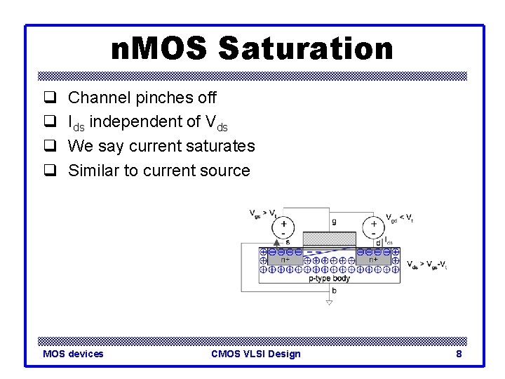
n. MOS Saturation q q Channel pinches off Ids independent of Vds We say current saturates Similar to current source MOS devices CMOS VLSI Design 8

I-V Characteristics q In Linear region, Ids depends on – How much charge is in the channel? – How fast is the charge moving? MOS devices CMOS VLSI Design 9

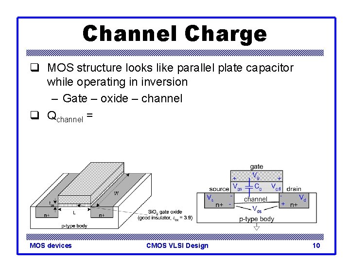
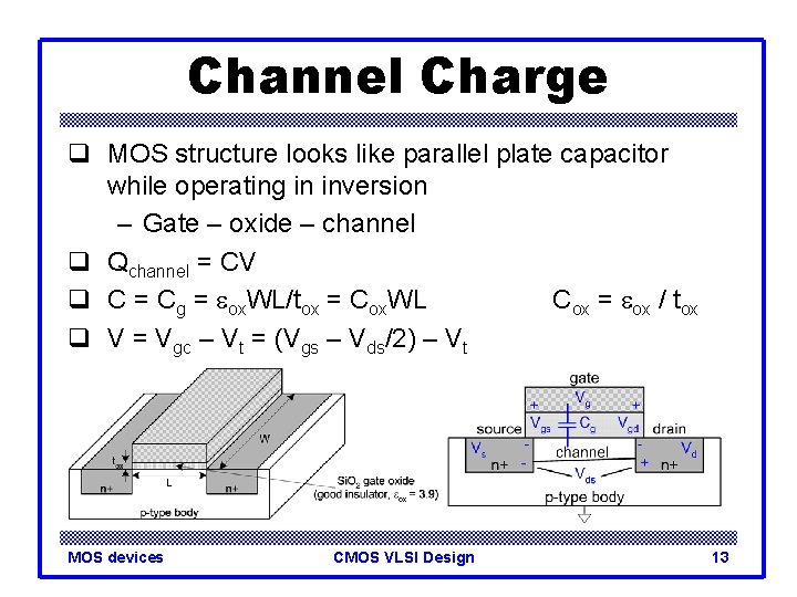
Channel Charge q MOS structure looks like parallel plate capacitor while operating in inversion – Gate – oxide – channel q Qchannel = MOS devices CMOS VLSI Design 10

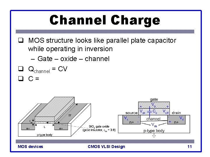
Channel Charge q MOS structure looks like parallel plate capacitor while operating in inversion – Gate – oxide – channel q Qchannel = CV q C= MOS devices CMOS VLSI Design 11

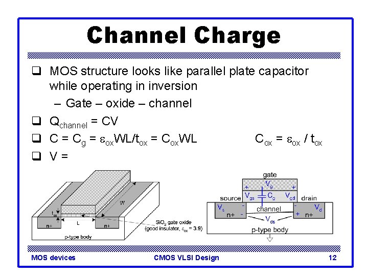
Channel Charge q MOS structure looks like parallel plate capacitor while operating in inversion – Gate – oxide – channel q Qchannel = CV Cox = eox / tox q C = Cg = eox. WL/tox = Cox. WL q V= MOS devices CMOS VLSI Design 12

Channel Charge q MOS structure looks like parallel plate capacitor while operating in inversion – Gate – oxide – channel q Qchannel = CV Cox = eox / tox q C = Cg = eox. WL/tox = Cox. WL q V = Vgc – Vt = (Vgs – Vds/2) – Vt MOS devices CMOS VLSI Design 13

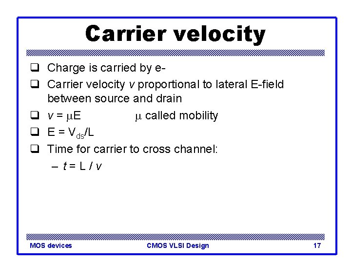
Carrier velocity q Charge is carried by eq Carrier velocity v proportional to lateral E-field between source and drain q v= MOS devices CMOS VLSI Design 14

Carrier velocity q Charge is carried by eq Carrier velocity v proportional to lateral E-field between source and drain q v = m. E m called mobility q E= MOS devices CMOS VLSI Design 15

Carrier velocity q Charge is carried by eq Carrier velocity v proportional to lateral E-field between source and drain q v = m. E m called mobility q E = Vds/L q Time for carrier to cross channel: – t= MOS devices CMOS VLSI Design 16

Carrier velocity q Charge is carried by eq Carrier velocity v proportional to lateral E-field between source and drain q v = m. E m called mobility q E = Vds/L q Time for carrier to cross channel: – t=L/v MOS devices CMOS VLSI Design 17

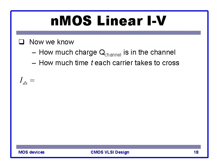
n. MOS Linear I-V q Now we know – How much charge Qchannel is in the channel – How much time t each carrier takes to cross MOS devices CMOS VLSI Design 18

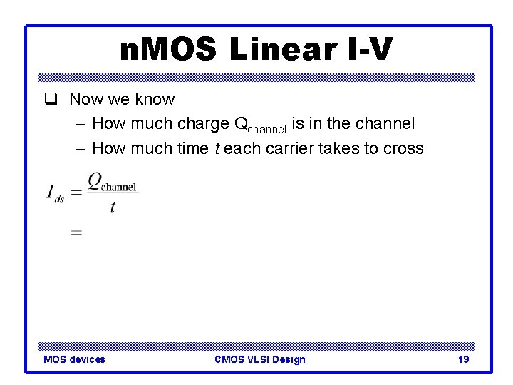
n. MOS Linear I-V q Now we know – How much charge Qchannel is in the channel – How much time t each carrier takes to cross MOS devices CMOS VLSI Design 19

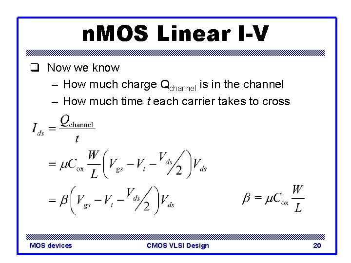
n. MOS Linear I-V q Now we know – How much charge Qchannel is in the channel – How much time t each carrier takes to cross MOS devices CMOS VLSI Design 20

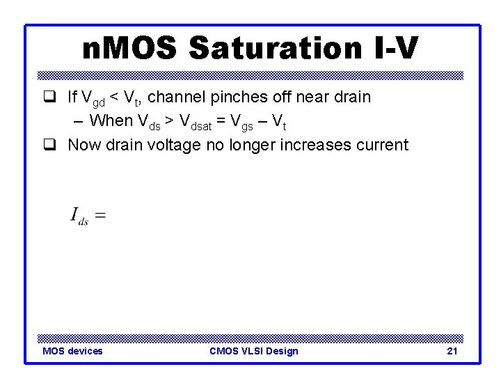
n. MOS Saturation I-V q If Vgd < Vt, channel pinches off near drain – When Vds > Vdsat = Vgs – Vt q Now drain voltage no longer increases current MOS devices CMOS VLSI Design 21

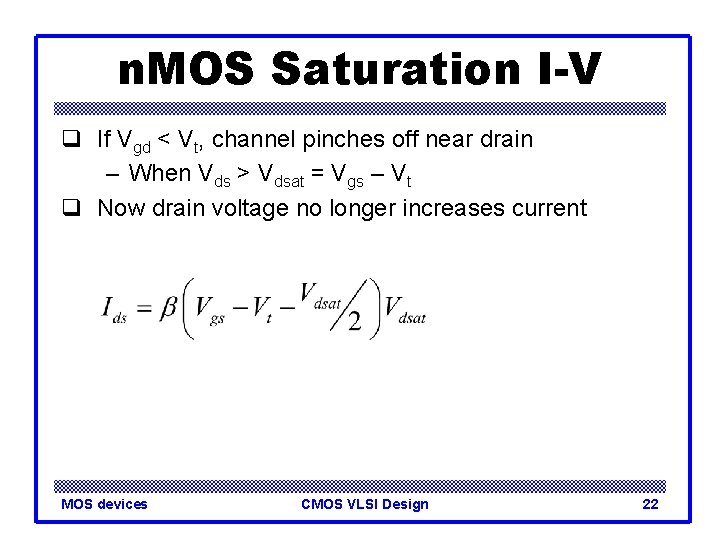
n. MOS Saturation I-V q If Vgd < Vt, channel pinches off near drain – When Vds > Vdsat = Vgs – Vt q Now drain voltage no longer increases current MOS devices CMOS VLSI Design 22

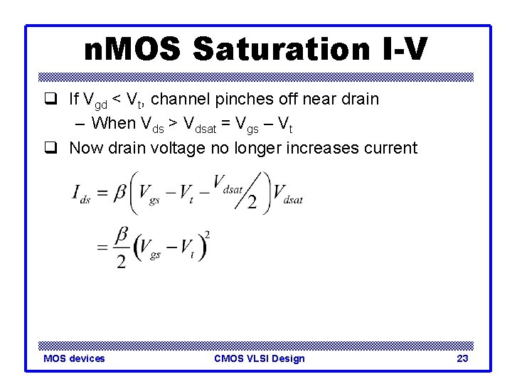
n. MOS Saturation I-V q If Vgd < Vt, channel pinches off near drain – When Vds > Vdsat = Vgs – Vt q Now drain voltage no longer increases current MOS devices CMOS VLSI Design 23

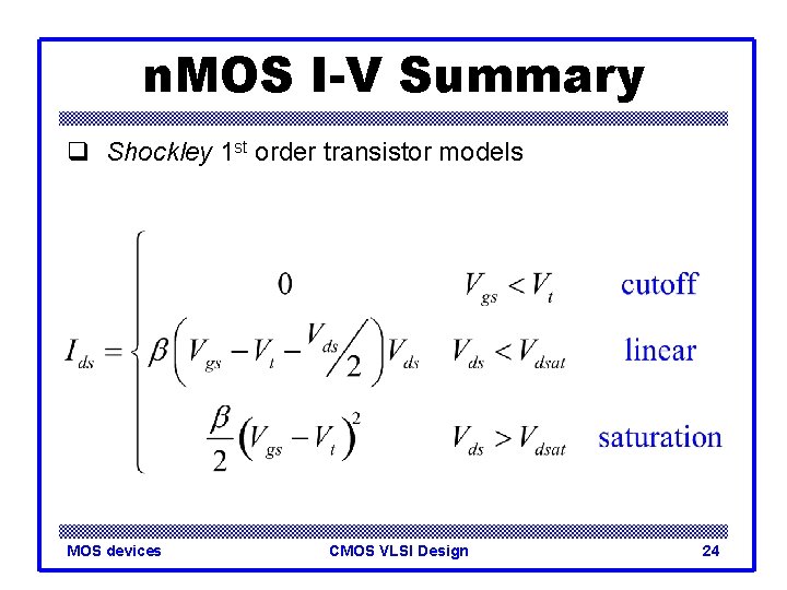
n. MOS I-V Summary q Shockley 1 st order transistor models MOS devices CMOS VLSI Design 24

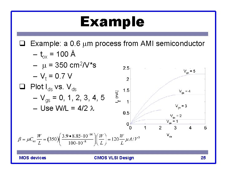
Example q Example: a 0. 6 mm process from AMI semiconductor – tox = 100 Å – m = 350 cm 2/V*s – Vt = 0. 7 V q Plot Ids vs. Vds – Vgs = 0, 1, 2, 3, 4, 5 – Use W/L = 4/2 l MOS devices CMOS VLSI Design 25

p. MOS I-V q All dopings and voltages are inverted for p. MOS q Mobility mp is determined by holes – Typically 2 -3 x lower than that of electrons mn – 120 cm 2/V*s in AMI 0. 6 mm process q Thus p. MOS must be wider to provide same current – In this class, assume mn / mp = 2 MOS devices CMOS VLSI Design 26

Capacitance q Any two conductors separated by an insulator have capacitance q Gate to channel capacitor is very important – Creates channel charge necessary for operation q Source and drain have capacitance to body – Across reverse-biased diodes – Called diffusion capacitance because it is associated with source/drain diffusion MOS devices CMOS VLSI Design 27

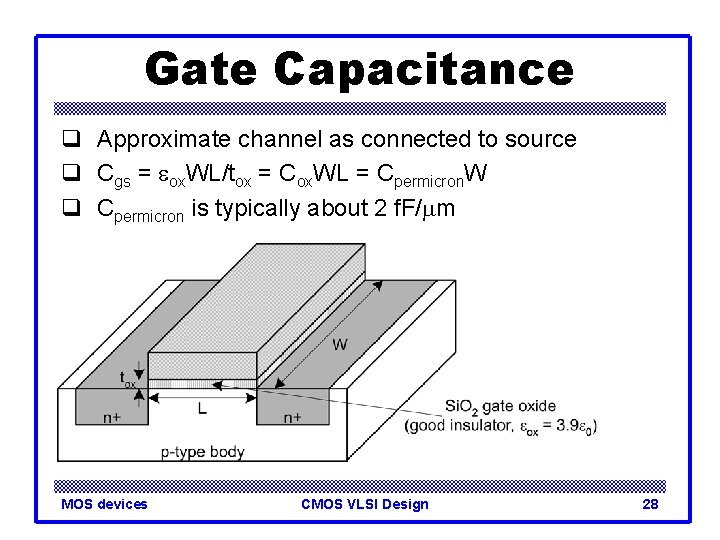
Gate Capacitance q Approximate channel as connected to source q Cgs = eox. WL/tox = Cox. WL = Cpermicron. W q Cpermicron is typically about 2 f. F/mm MOS devices CMOS VLSI Design 28

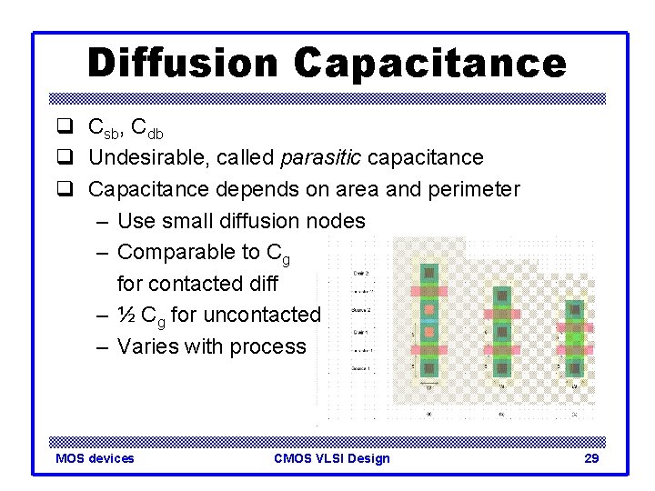
Diffusion Capacitance q Csb, Cdb q Undesirable, called parasitic capacitance q Capacitance depends on area and perimeter – Use small diffusion nodes – Comparable to Cg for contacted diff – ½ Cg for uncontacted – Varies with process MOS devices CMOS VLSI Design 29

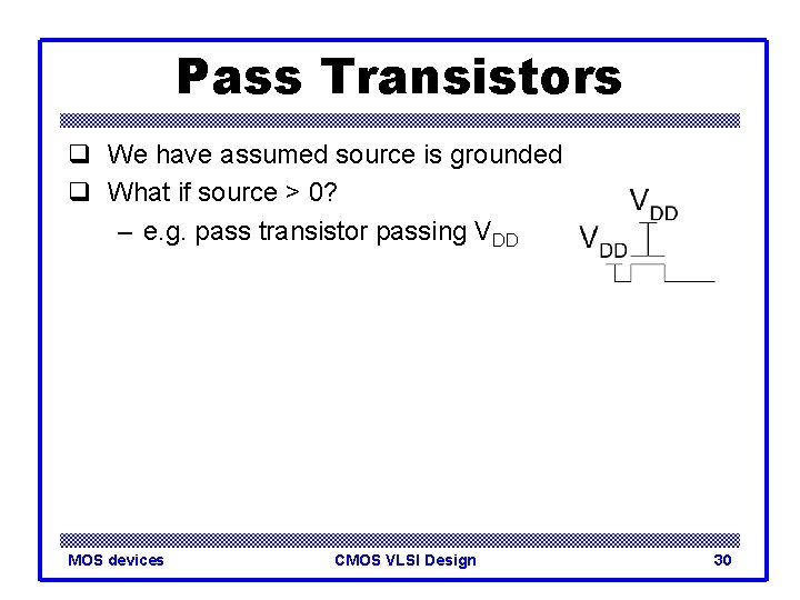
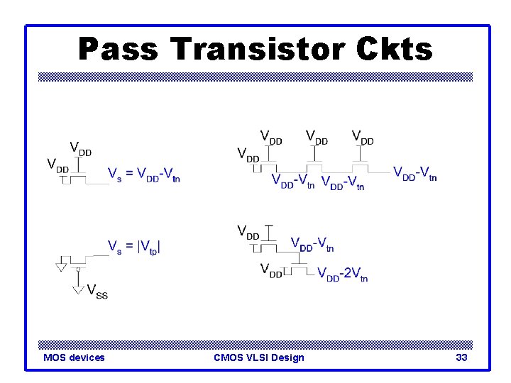
Pass Transistors q We have assumed source is grounded q What if source > 0? – e. g. pass transistor passing VDD MOS devices CMOS VLSI Design 30

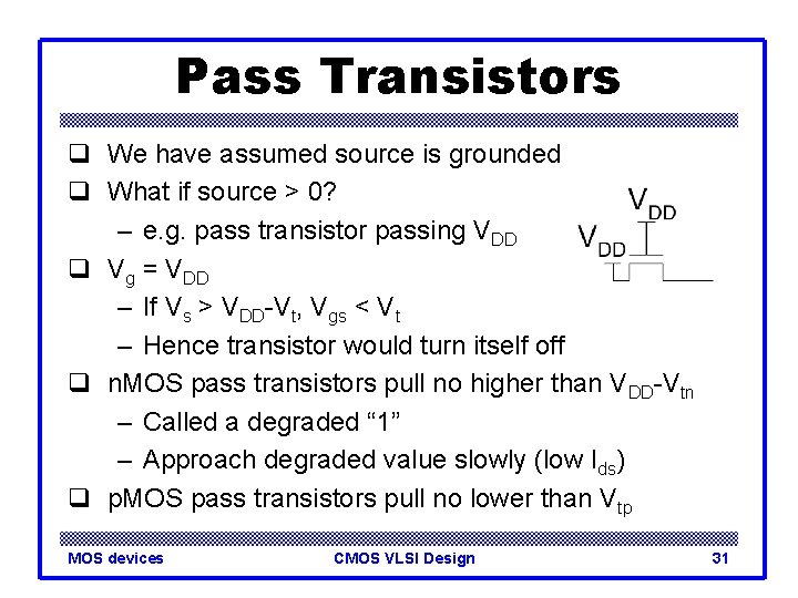
Pass Transistors q We have assumed source is grounded q What if source > 0? – e. g. pass transistor passing VDD q Vg = VDD – If Vs > VDD-Vt, Vgs < Vt – Hence transistor would turn itself off q n. MOS pass transistors pull no higher than VDD-Vtn – Called a degraded “ 1” – Approach degraded value slowly (low Ids) q p. MOS pass transistors pull no lower than Vtp MOS devices CMOS VLSI Design 31

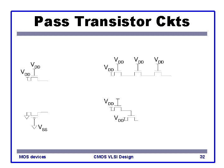
Pass Transistor Ckts MOS devices CMOS VLSI Design 32

Pass Transistor Ckts MOS devices CMOS VLSI Design 33

Effective Resistance q Shockley models have limited value – Not accurate enough for modern transistors – Too complicated for much hand analysis q Simplification: treat transistor as resistor – Replace Ids(Vds, Vgs) with effective resistance R • Ids = Vds/R – R averaged across switching of digital gate q Too inaccurate to predict current at any given time – But good enough to predict RC delay MOS devices CMOS VLSI Design 34

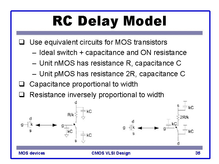
RC Delay Model q Use equivalent circuits for MOS transistors – Ideal switch + capacitance and ON resistance – Unit n. MOS has resistance R, capacitance C – Unit p. MOS has resistance 2 R, capacitance C q Capacitance proportional to width q Resistance inversely proportional to width MOS devices CMOS VLSI Design 35

RC Values q Capacitance – C = Cg = Cs = Cd = 2 f. F/mm of gate width – Values similar across many processes q Resistance – R 6 KW*mm in 0. 6 um process – Improves with shorter channel lengths q Unit transistors – May refer to minimum contacted device (4/2 l) – Or maybe 1 mm wide device – Doesn’t matter as long as you are consistent MOS devices CMOS VLSI Design 36

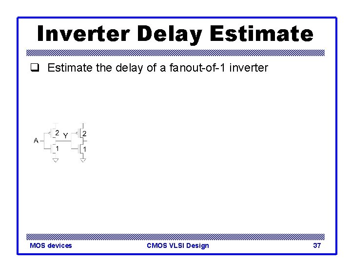
Inverter Delay Estimate q Estimate the delay of a fanout-of-1 inverter MOS devices CMOS VLSI Design 37

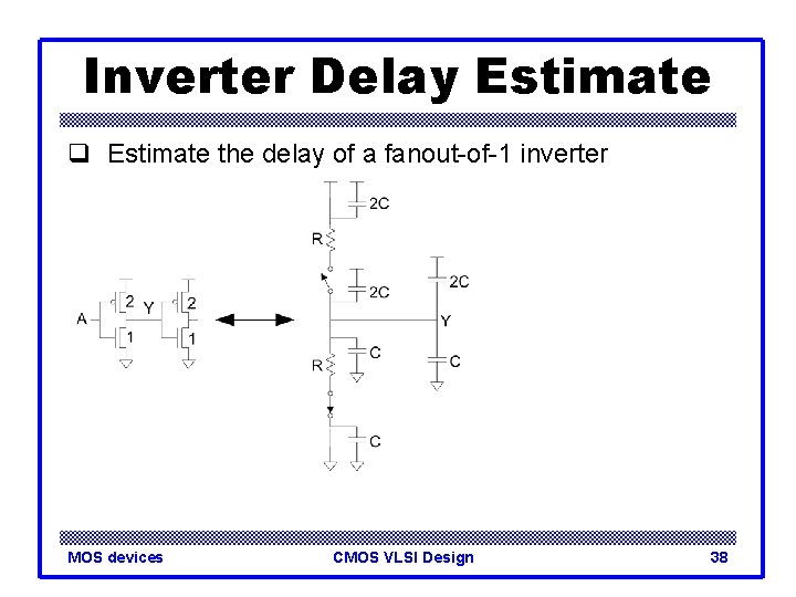
Inverter Delay Estimate q Estimate the delay of a fanout-of-1 inverter MOS devices CMOS VLSI Design 38

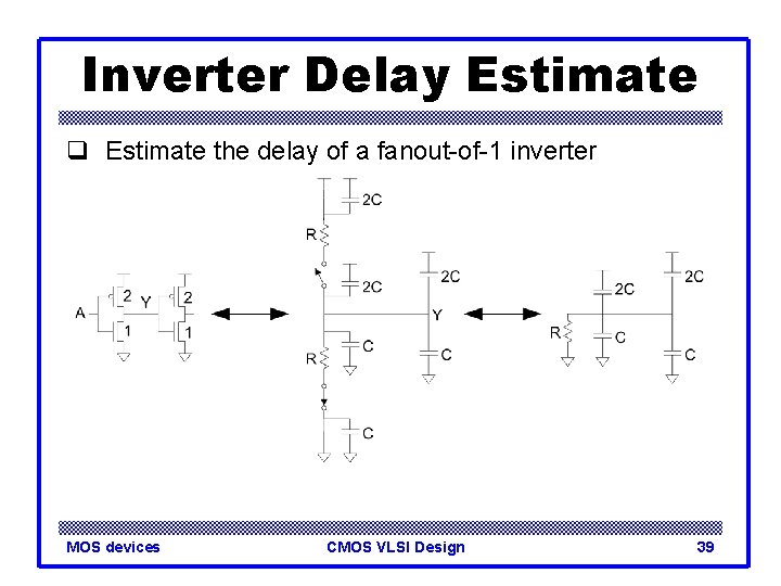
Inverter Delay Estimate q Estimate the delay of a fanout-of-1 inverter MOS devices CMOS VLSI Design 39

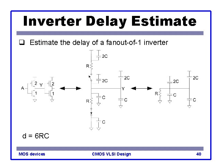
Inverter Delay Estimate q Estimate the delay of a fanout-of-1 inverter d = 6 RC MOS devices CMOS VLSI Design 40