Chapter 6 Serial Interface UART universal asynchronous receiver
![Step 2: U 0 FCR--FIFO control set reg=0 x 07 [U 0 FCR]=0 x Step 2: U 0 FCR--FIFO control set reg=0 x 07 [U 0 FCR]=0 x](https://slidetodoc.com/presentation_image_h2/0946a0aaf763668240174645eee85376/image-31.jpg)


- Slides: 43

Chapter 6: Serial Interface -UART (universal asynchronous receiver transmitter ) CEG 2400 - Microcomputer Systems CEG 2400 Ch 6. Serial Interface -- UART V 7 b 1 1

Overview 1. Introduction to the universal asynchronous receiver transmitter : UART. 2. UART Hardware Interface 3. UART Software Interface 4. Initialize the UART Hardware 5. Sending data using handshaking CEG 2400 Ch 6. Serial Interface -- UART V 7 b 2 2

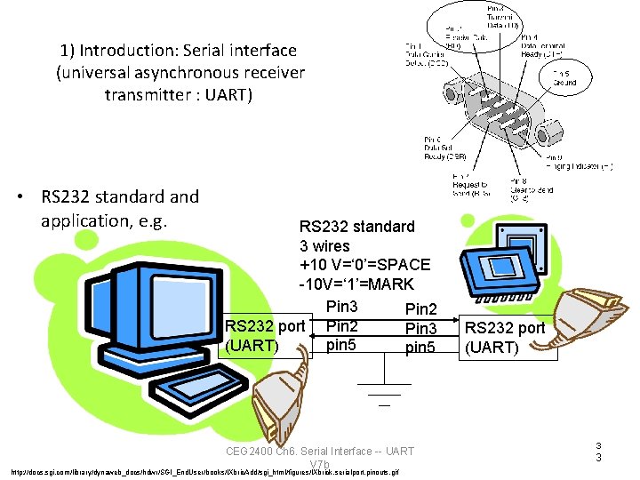
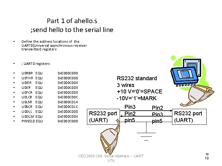
1) Introduction: Serial interface (universal asynchronous receiver transmitter : UART) • RS 232 standard and application, e. g. RS 232 standard 3 wires +10 V=‘ 0’=SPACE -10 V=‘ 1’=MARK Pin 3 Pin 2 RS 232 port Pin 2 Pin 3 pin 5 (UART) pin 5 CEG 2400 Ch 6. Serial Interface -- UART V 7 b http: //docs. sgi. com/library/dynaweb_docs/hdwr/SGI_End. User/books/IXbric. Add/sgi_html/figures/IXbrick. serialport. pinouts. gif RS 232 port (UART) 3 3

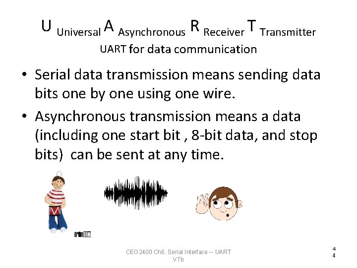
U Universal A Asynchronous R Receiver T Transmitter UART for data communication • Serial data transmission means sending data bits one by one using one wire. • Asynchronous transmission means a data (including one start bit , 8 -bit data, and stop bits) can be sent at any time. CEG 2400 Ch 6. Serial Interface -- UART V 7 b 4 4

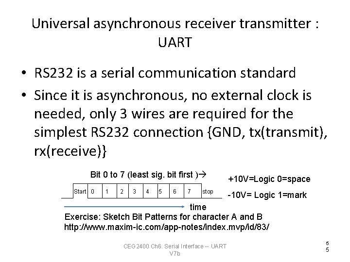
Universal asynchronous receiver transmitter : UART • RS 232 is a serial communication standard • Since it is asynchronous, no external clock is needed, only 3 wires are required for the simplest RS 232 connection {GND, tx(transmit), rx(receive)} Bit 0 to 7 (least sig. bit first ) Start 0 1 2 3 4 5 6 7 stop +10 V=Logic 0=space -10 V= Logic 1=mark time Exercise: Sketch Bit Patterns for character A and B http: //www. maxim-ic. com/app-notes/index. mvp/id/83/ CEG 2400 Ch 6. Serial Interface -- UART V 7 b 5 5

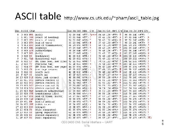
ASCII table http: //www. cs. utk. edu/~pham/ascii_table. jpg CEG 2400 Ch 6. Serial Interface -- UART V 7 b 6 6

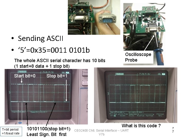
EXAMPLES • Sending ASCII • ‘ 5’=0 x 35=0011 0101 b The whole ASCII serial character has 10 bits (1 start+8 data + 1 stop bit) Start bit=0 T=bit period =1/baud rate Oscilloscope Probe Stop bit=1 10101100(stop bit=1) Least Sign. Bit first What is this code ? CEG 2400 Ch 6. Serial Interface -- UART V 7 b 7 7

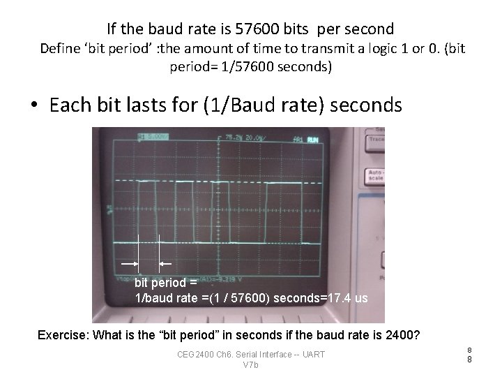
If the baud rate is 57600 bits per second Define ‘bit period’ : the amount of time to transmit a logic 1 or 0. (bit period= 1/57600 seconds) • Each bit lasts for (1/Baud rate) seconds bit period = 1/baud rate =(1 / 57600) seconds=17. 4 us Exercise: What is the “bit period” in seconds if the baud rate is 2400? CEG 2400 Ch 6. Serial Interface -- UART V 7 b 8 8

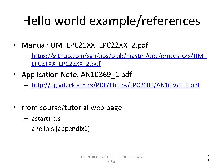
Hello world example/references • Manual: UM_LPC 21 XX_LPC 22 XX_2. pdf – https: //github. com/sgh/aos/blob/master/doc/processors/UM_ LPC 21 XX_LPC 22 XX_2. pdf • Application Note: AN 10369_1. pdf – http: //uglyduck. ath. cx/PDF/Philips/LPC 2000/AN 10369_1. pdf • from course/tutorial web page – astartup. s – ahello. s (appendix 1) CEG 2400 Ch 6. Serial Interface -- UART V 7 b 9 9

2) UART Hardware Interface CEG 2400 Ch 6. Serial Interface -- UART V 7 b 10 10

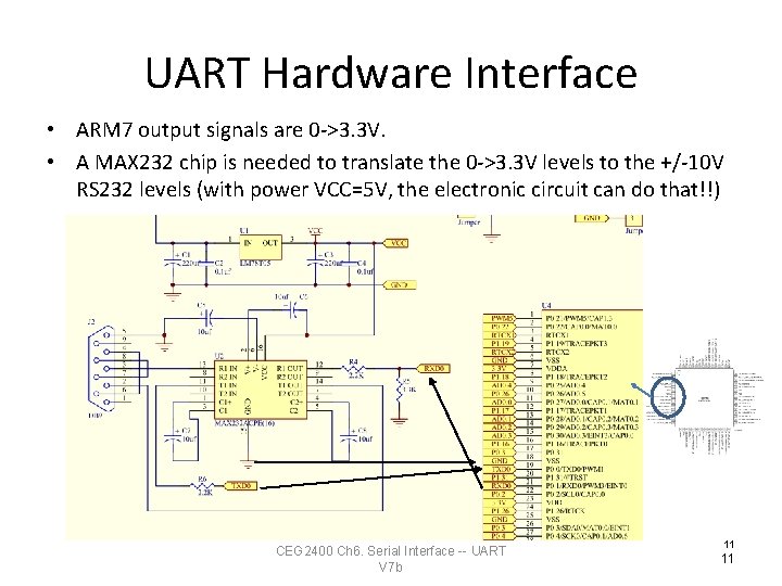
UART Hardware Interface • ARM 7 output signals are 0 ->3. 3 V. • A MAX 232 chip is needed to translate the 0 ->3. 3 V levels to the +/-10 V RS 232 levels (with power VCC=5 V, the electronic circuit can do that!!) CEG 2400 Ch 6. Serial Interface -- UART V 7 b 11 11

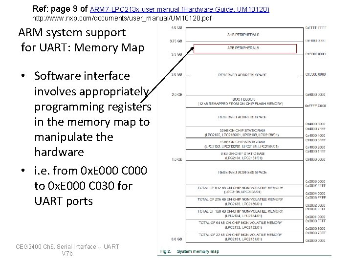
Ref: page 9 of ARM 7 -LPC 213 x-user manual (Hardware Guide, UM 10120) http: //www. nxp. com/documents/user_manual/UM 10120. pdf ARM system support for UART: Memory Map • Software interface involves appropriately programming registers in the memory map to manipulate the hardware • i. e. from 0 x. E 000 C 000 to 0 x. E 000 C 030 for UART ports CEG 2400 Ch 6. Serial Interface -- UART V 7 b • 12 12

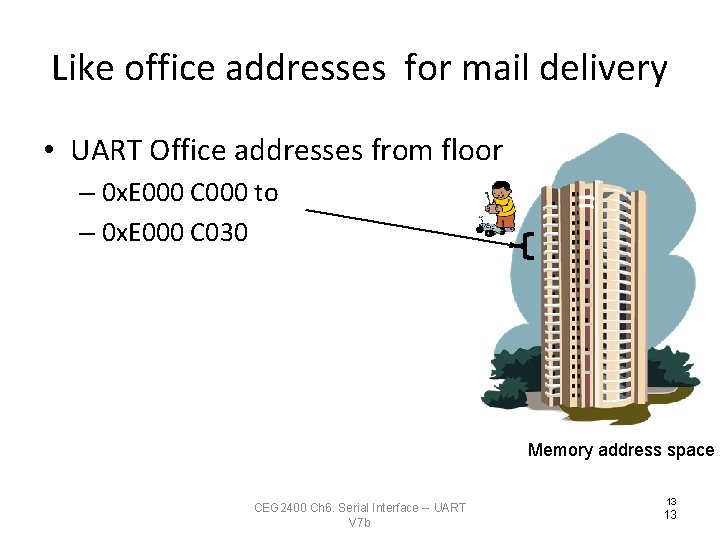
Like office addresses for mail delivery • UART Office addresses from floor – 0 x. E 000 C 000 to – 0 x. E 000 C 030 Memory address space CEG 2400 Ch 6. Serial Interface -- UART V 7 b 13 13

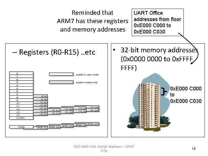
Reminded that ARM 7 has these registers and memory addresses – Registers (R 0 -R 15). . etc UART Office addresses from floor 0 x. E 000 C 000 to 0 x. E 000 C 030 • 32 -bit memory addresses (0 x 0000 to 0 x. FFFF) 0 x. E 000 C 000 to 0 x. E 000 C 030 CEG 2400 Ch 6. Serial Interface -- UART V 7 b 14

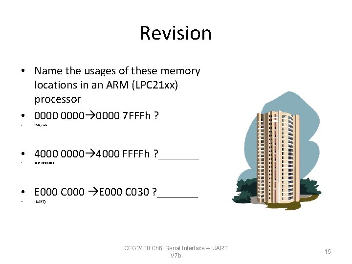
Revision • Name the usages of these memory locations in an ARM (LPC 21 xx) processor • 0000 7 FFFh ? _______ • ROM, code • 4000 0000 4000 FFFFh ? _______ • RAM, data, Stack • E 000 C 000 E 000 C 030 ? _______ • (UART) CEG 2400 Ch 6. Serial Interface -- UART V 7 b 15

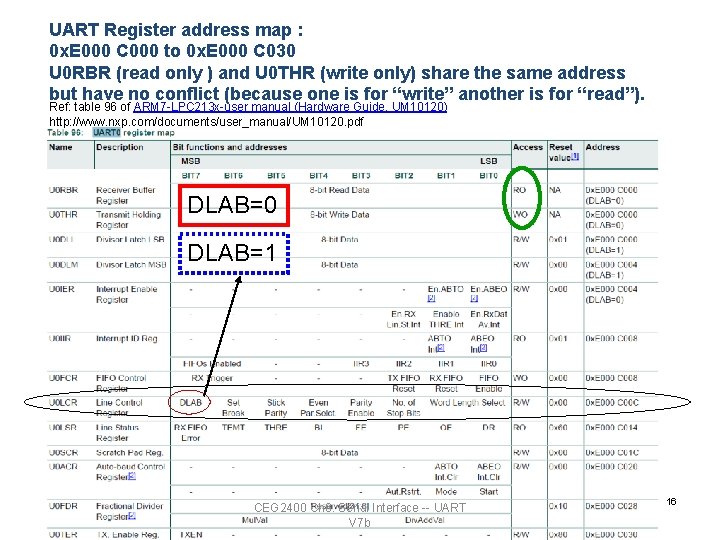
UART Register address map : 0 x. E 000 C 000 to 0 x. E 000 C 030 U 0 RBR (read only ) and U 0 THR (write only) share the same address but have no conflict (because one is for “write” another is for “read”). Ref: table 96 of ARM 7 -LPC 213 x-user manual (Hardware Guide, UM 10120) http: //www. nxp. com/documents/user_manual/UM 10120. pdf • DLAB=0 DLAB=1 CEG 2400 Ch 6. Serial Interface -- UART V 7 b 16 16

3) UART A general description of the software Interface ahello. s http: //www. cse. cuhk. edu. hk/%7 Ekhwong/www 2/ceng 2400/ahello. s CEG 2400 Ch 6. Serial Interface -- UART V 7 b 17 17

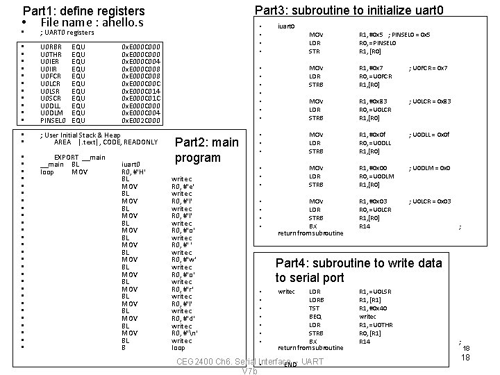
Part 3: subroutine to initialize uart 0 Part 1: define registers • • File name : ahello. s • • ; UART 0 registers • • • U 0 RBR U 0 THR U 0 IER U 0 IIR U 0 FCR U 0 LSR U 0 SCR U 0 DLL U 0 DLM PINSEL 0 EQU EQU EQU 0 x. E 000 C 000 0 x. E 000 C 004 0 x. E 000 C 008 0 x. E 000 C 014 0 x. E 000 C 01 C 0 x. E 000 C 000 0 x. E 000 C 004 0 x. E 002 C 000 • • ; User Initial Stack & Heap AREA |. text|, CODE, READONLY • • • • • • • EXPORT __main BL loop MOV iuart 0 R 0, #'H' BL MOV BL MOV BL MOV BL B Part 2: main program writec R 0, #'e' writec R 0, #'l' writec R 0, #'o' writec R 0, #'w' writec R 0, #'o' writec R 0, #'r' writec R 0, #'l' writec R 0, #'d' writec R 0, #'n' writec loop iuart 0 MOV LDR STR R 1, #0 x 5 ; PINSEL 0 = 0 x 5 R 0, =PINSEL 0 R 1, [R 0] • • MOV LDR STRB R 1, #0 x 7 R 0, =U 0 FCR R 1, [R 0] ; U 0 FCR = 0 x 7 MOV LDR STRB R 1, #0 x 83 R 0, =U 0 LCR R 1, [R 0] ; U 0 LCR = 0 x 83 • • • MOV LDR STRB R 1, #0 x 0 f R 0, =U 0 DLL R 1, [R 0] ; U 0 DLL = 0 x 0 f • • • MOV LDR STRB R 1, #0 x 00 R 0, =U 0 DLM R 1, [R 0] ; U 0 DLM = 0 x 0 R 1, #0 x 03 R 0, =U 0 LCR R 1, [R 0] R 14 ; U 0 LCR = 0 x 03 • • MOV LDR STRB BX return from subroutine ; Part 4: subroutine to write data to serial port • • writec LDRB TST BEQ LDR STRB BX return from subroutine CEG 2400 Ch 6. Serial Interface • END-- UART V 7 b R 1, =U 0 LSR R 1, [R 1] R 1, #0 x 40 writec R 1, =U 0 THR R 0, [R 1] R 14 ; 18 18

Part 1 of ahello. s ; send hello to the serial line • Define the address locations of the UART 0(Universal asynchronous receiver transmitter) registers • ; UART 0 registers • • • U 0 RBR EQU U 0 THR EQU U 0 IER EQU U 0 IIR EQU U 0 FCR EQU U 0 LSR EQU U 0 SCR EQU U 0 DLL EQU U 0 DLM EQU PINSEL 0 EQU 0 x. E 000 C 000 0 x. E 000 C 004 0 x. E 000 C 008 0 x. E 000 C 014 0 x. E 000 C 01 C 0 x. E 000 C 000 0 x. E 000 C 004 0 x. E 002 C 000 RS 232 standard 3 wires +10 V=‘ 0’=SPACE -10 V=‘ 1’=MARK RS 232 port (UART) Pin 3 Pin 2 pin 5 CEG 2400 Ch 6. Serial Interface -- UART V 7 b Pin 2 Pin 3 pin 5 RS 232 port (UART) 19 19

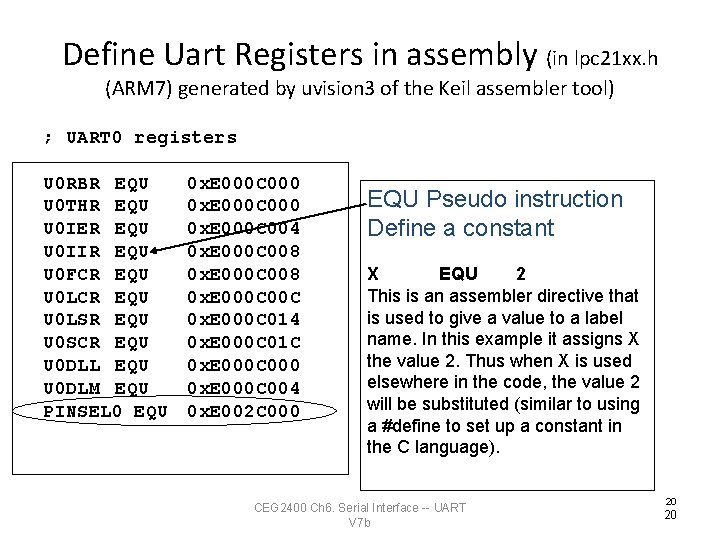
Define Uart Registers in assembly (in lpc 21 xx. h (ARM 7) generated by uvision 3 of the Keil assembler tool) ; UART 0 registers U 0 RBR EQU U 0 THR EQU U 0 IER EQU U 0 IIR EQU U 0 FCR EQU U 0 LSR EQU U 0 SCR EQU U 0 DLL EQU U 0 DLM EQU PINSEL 0 EQU 0 x. E 000 C 000 0 x. E 000 C 004 0 x. E 000 C 008 0 x. E 000 C 014 0 x. E 000 C 01 C 0 x. E 000 C 000 0 x. E 000 C 004 0 x. E 002 C 000 EQU Pseudo instruction Define a constant X EQU 2 This is an assembler directive that is used to give a value to a label name. In this example it assigns X the value 2. Thus when X is used elsewhere in the code, the value 2 will be substituted (similar to using a #define to set up a constant in the C language). CEG 2400 Ch 6. Serial Interface -- UART V 7 b 20 20

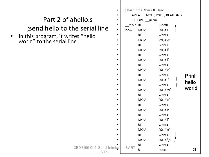
• ; User Initial Stack & Heap • AREA |. text|, CODE, READONLY • EXPORT __main • __main BL iuart 0 • loop MOV R 0, #'H' • BL writec In this program, it writes “hello • MOV R 0, #'e' world” to the serial line. • BL writec • MOV R 0, #'l' • BL writec • MOV R 0, #'o' • BL writec • MOV R 0, #'w' • BL writec • MOV R 0, #'o' • BL writec • MOV R 0, #'r' • BL writec • MOV R 0, #'l' • BL writec • MOV R 0, #'d' • BL writec • MOV R 0, #'n' • BL writec CEG 2400 Ch 6. Serial Interface -- UART • B loop Part 2 of ahello. s ; send hello to the serial line • V 7 b Print hello world 21

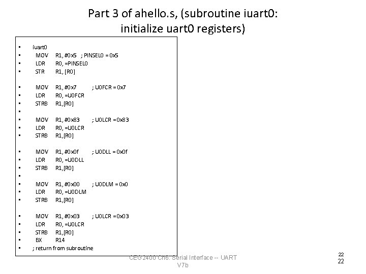
Part 3 of ahello. s, (subroutine iuart 0: initialize uart 0 registers) • • iuart 0 MOV LDR STR • • MOV LDR STRB R 1, #0 x 7 R 0, =U 0 FCR R 1, [R 0] ; U 0 FCR = 0 x 7 MOV LDR STRB R 1, #0 x 83 R 0, =U 0 LCR R 1, [R 0] ; U 0 LCR = 0 x 83 • • MOV LDR STRB R 1, #0 x 0 f R 0, =U 0 DLL R 1, [R 0] ; U 0 DLL = 0 x 0 f MOV LDR STRB R 1, #0 x 00 ; U 0 DLM = 0 x 0 R 0, =U 0 DLM R 1, [R 0] • • • R 1, #0 x 5 ; PINSEL 0 = 0 x 5 R 0, =PINSEL 0 R 1, [R 0] MOV R 1, #0 x 03 ; U 0 LCR = 0 x 03 LDR R 0, =U 0 LCR STRB R 1, [R 0] BX R 14 ; return from subroutine CEG 2400 Ch 6. Serial Interface -- UART V 7 b 22 22

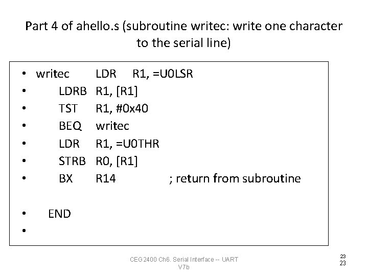
Part 4 of ahello. s (subroutine writec: write one character to the serial line) • writec • LDRB • TST • BEQ • LDR • STRB • BX • • LDR R 1, =U 0 LSR R 1, [R 1] R 1, #0 x 40 writec R 1, =U 0 THR R 0, [R 1] R 14 ; return from subroutine END CEG 2400 Ch 6. Serial Interface -- UART V 7 b 23 23

4) Detailed description of subroutines “iuart 0” in ahello. s Initialize the UART Hardware Setup data into UART registers 0 x. E 000 C 000 to 0 x. E 000 C 030 CEG 2400 Ch 6. Serial Interface -- UART V 7 b 24 24

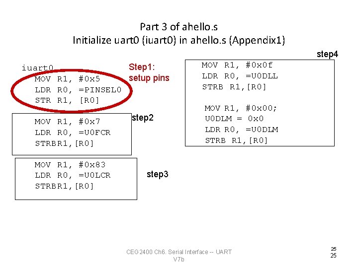
Part 3 of ahello. s Initialize uart 0 (iuart 0) in ahello. s (Appendix 1) step 4 Step 1: iuart 0 setup pins MOV R 1, #0 x 5 LDR R 0, =PINSEL 0 STR R 1, [R 0] MOV R 1, #0 x 7 LDR R 0, =U 0 FCR STRB R 1, [R 0] MOV R 1, #0 x 83 LDR R 0, =U 0 LCR STRB R 1, [R 0] step 2 MOV R 1, #0 x 0 f LDR R 0, =U 0 DLL STRB R 1, [R 0] MOV R 1, #0 x 00; U 0 DLM = 0 x 0 LDR R 0, =U 0 DLM STRB R 1, [R 0] step 3 CEG 2400 Ch 6. Serial Interface -- UART V 7 b 25 25

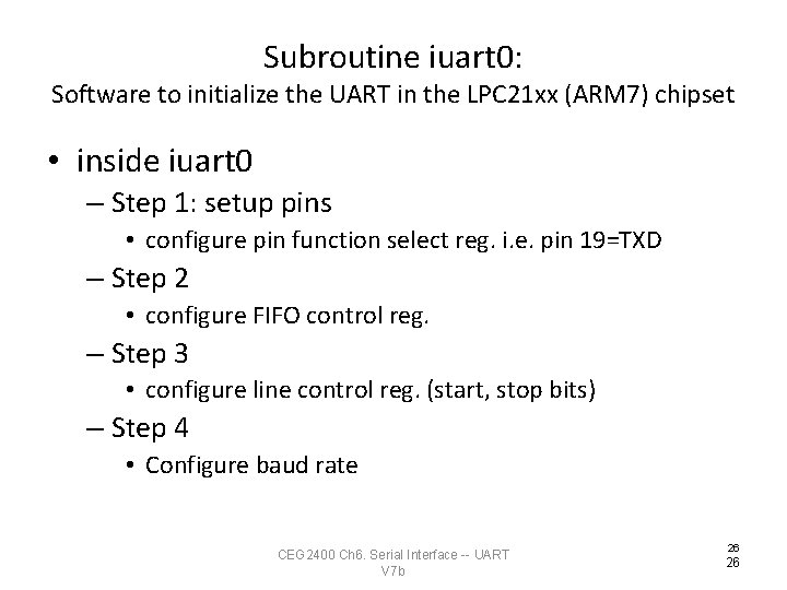
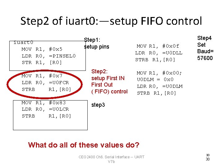
Subroutine iuart 0: Software to initialize the UART in the LPC 21 xx (ARM 7) chipset • inside iuart 0 – Step 1: setup pins • configure pin function select reg. i. e. pin 19=TXD – Step 2 • configure FIFO control reg. – Step 3 • configure line control reg. (start, stop bits) – Step 4 • Configure baud rate CEG 2400 Ch 6. Serial Interface -- UART V 7 b 26 26

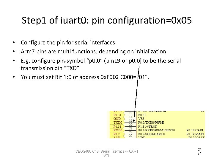
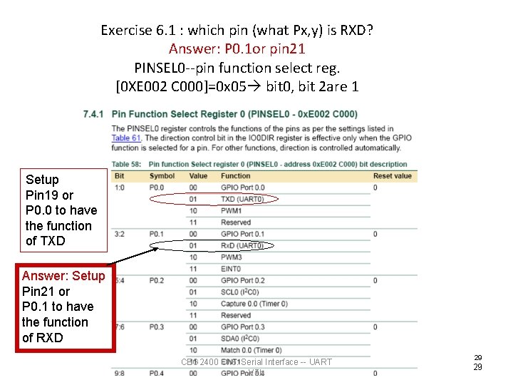
Step 1 of iuart 0: pin configuration=0 x 05 • Configure the pin for serial interfaces • Arm 7 pins are multi functions, depending on initialization. • E. g. configure pin-symbol “p 0. 0” (pin 19 or p 0. 0) to be the serial transmission pin “TXD” • You must set Bit 1: 0 of address 0 x. E 002 C 000=“ 01”. CEG 2400 Ch 6. Serial Interface -- UART V 7 b 27 27

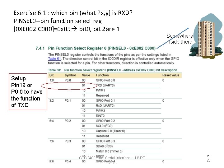
Exercise 6. 1 : which pin (what Px, y) is RXD? PINSEL 0 --pin function select reg. [0 XE 002 C 000]=0 x 05 bit 0, bit 2 are 1 Somewhere inside there Setup Pin 19 or P 0. 0 to have the function of TXD CEG 2400 Ch 6. Serial Interface -- UART V 7 b 28 28

Exercise 6. 1 : which pin (what Px, y) is RXD? Answer: P 0. 1 or pin 21 PINSEL 0 --pin function select reg. [0 XE 002 C 000]=0 x 05 bit 0, bit 2 are 1 Setup Pin 19 or P 0. 0 to have the function of TXD Answer: Setup Pin 21 or P 0. 1 to have the function of RXD CEG 2400 Ch 6. Serial Interface -- UART V 7 b 29 29

Step 2 of iuart 0: —setup FIFO control iuart 0 MOV R 1, #0 x 5 LDR R 0, =PINSEL 0 STR R 1, [R 0] MOV R 1, #0 x 7 LDR R 0, =U 0 FCR STRB R 1, [R 0] MOV R 1, #0 x 83 LDR R 0, =U 0 LCR STRB R 1, [R 0] Step 1: setup pins Step 2: setup First IN First Out ( FIFO) control MOV R 1, #0 x 0 f LDR R 0, =U 0 DLL STRB R 1, [R 0] Step 4 Set Baud= 57600 MOV R 1, #0 x 00; U 0 DLM = 0 x 0 LDR R 0, =U 0 DLM STRB R 1, [R 0] step 3 What do all of these values do? CEG 2400 Ch 6. Serial Interface -- UART V 7 b 30 30
![Step 2 U 0 FCRFIFO control set reg0 x 07 U 0 FCR0 x Step 2: U 0 FCR--FIFO control set reg=0 x 07 [U 0 FCR]=0 x](https://slidetodoc.com/presentation_image_h2/0946a0aaf763668240174645eee85376/image-31.jpg)
Step 2: U 0 FCR--FIFO control set reg=0 x 07 [U 0 FCR]=0 x 07 Set all bit 0, 1, 2=“ 111” for FIFO control CEG 2400 Ch 6. Serial Interface -- UART V 7 b 31 31

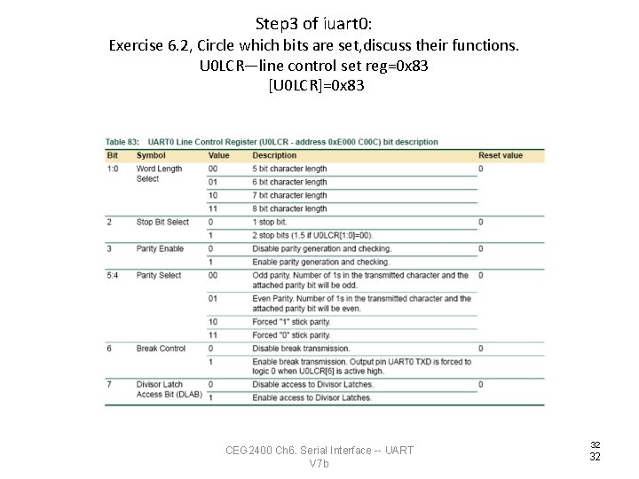
Step 3 of iuart 0: Exercise 6. 2, Circle which bits are set, discuss their functions. U 0 LCR—line control set reg=0 x 83 [U 0 LCR]=0 x 83 CEG 2400 Ch 6. Serial Interface -- UART V 7 b 32 32

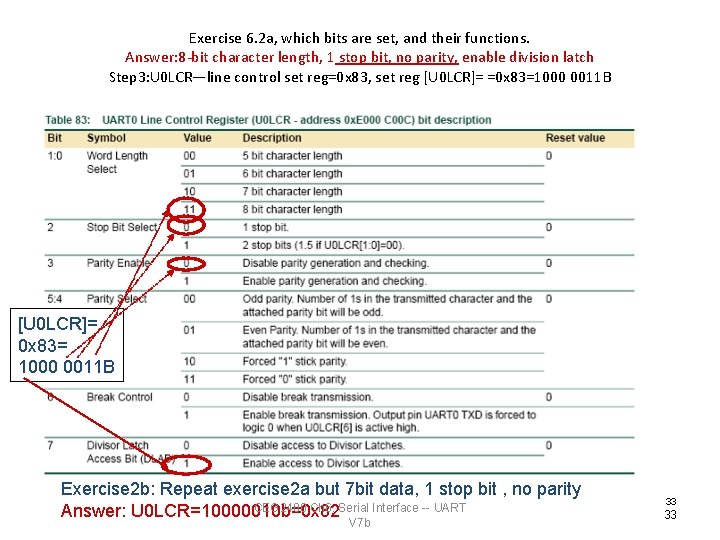
Exercise 6. 2 a, which bits are set, and their functions. Answer: 8 -bit character length, 1 stop bit, no parity, enable division latch Step 3: U 0 LCR—line control set reg=0 x 83, set reg [U 0 LCR]= =0 x 83=1000 0011 B [U 0 LCR]= 0 x 83= 1000 0011 B Exercise 2 b: Repeat exercise 2 a but 7 bit data, 1 stop bit , no parity CEG 2400 Ch 6. Serial Interface -- UART Answer: U 0 LCR=10000010 b=0 x 82 V 7 b 33 33

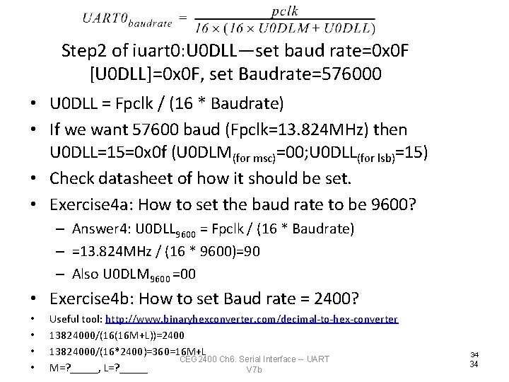
Step 2 of iuart 0: U 0 DLL—set baud rate=0 x 0 F [U 0 DLL]=0 x 0 F, set Baudrate=576000 • U 0 DLL = Fpclk / (16 * Baudrate) • If we want 57600 baud (Fpclk=13. 824 MHz) then U 0 DLL=15=0 x 0 f (U 0 DLM(for msc)=00; U 0 DLL(for lsb)=15) • Check datasheet of how it should be set. • Exercise 4 a: How to set the baud rate to be 9600? – Answer 4: U 0 DLL 9600 = Fpclk / (16 * Baudrate) – =13. 824 MHz / (16 * 9600)=90 – Also U 0 DLM 9600 =00 • Exercise 4 b: How to set Baud rate = 2400? • • Useful tool: http: //www. binaryhexconverter. com/decimal-to-hex-converter 13824000/(16(16 M+L))=2400 13824000/(16*2400)=360=16 M+L CEG 2400 Ch 6. Serial Interface -- UART M=? _____, L=? _____ V 7 b 34 34

5) Detailed description of subroutines “writec” : Sending data using handshaking CEG 2400 Ch 6. Serial Interface -- UART V 7 b 35 35

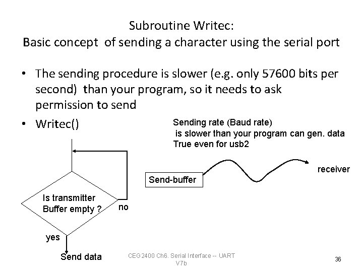
Subroutine Writec: Basic concept of sending a character using the serial port • The sending procedure is slower (e. g. only 57600 bits per second) than your program, so it needs to ask permission to send Sending rate (Baud rate) • Writec() is slower than your program can gen. data True even for usb 2 receiver Send-buffer Is transmitter Buffer empty ? no yes Send data CEG 2400 Ch 6. Serial Interface -- UART V 7 b 36

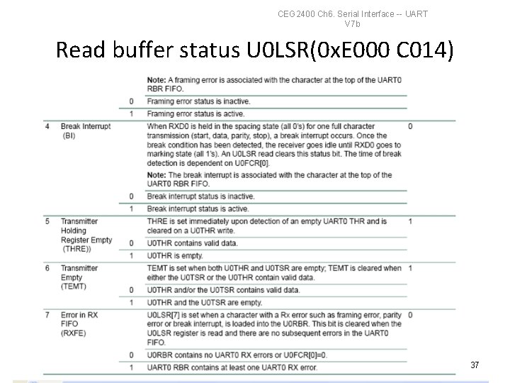
CEG 2400 Ch 6. Serial Interface -- UART V 7 b Read buffer status U 0 LSR(0 x. E 000 C 014) 37

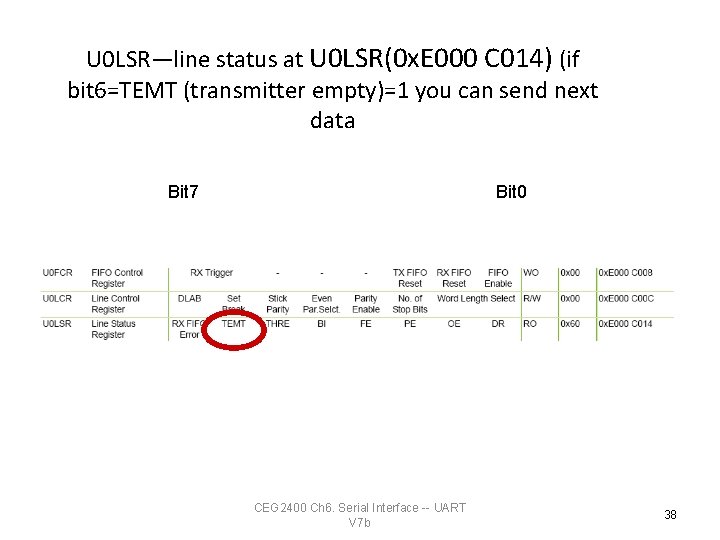
U 0 LSR—line status at U 0 LSR(0 x. E 000 C 014) (if bit 6=TEMT (transmitter empty)=1 you can send next data Bit 7 Bit 0 CEG 2400 Ch 6. Serial Interface -- UART V 7 b 38

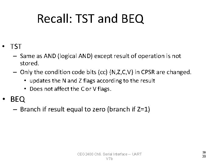
Recall: TST and BEQ • TST – Same as AND (logical AND) except result of operation is not stored. – Only the condition code bits (cc) {N, Z, C, V} in CPSR are changed. • updates the N and Z flags according to the result • Does not affect the C or V flags. • BEQ – Branch if result equal to zero (branch if Z=1) CEG 2400 Ch 6. Serial Interface -- UART V 7 b 39 39

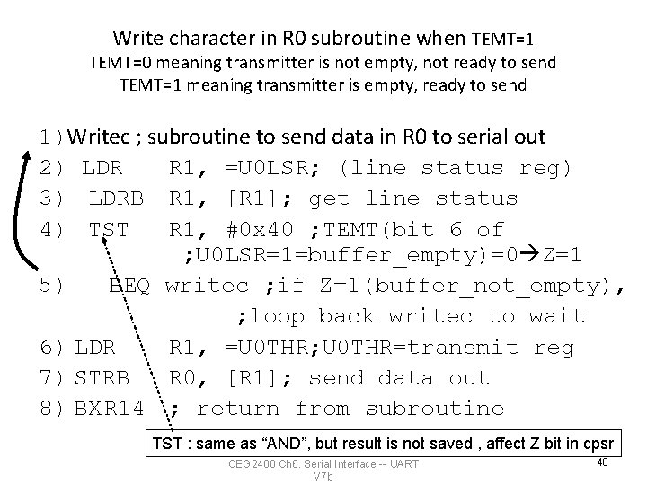
Write character in R 0 subroutine when TEMT=1 TEMT=0 meaning transmitter is not empty, not ready to send TEMT=1 meaning transmitter is empty, ready to send 1)Writec ; subroutine to send data in R 0 to serial out 2) LDR R 1, =U 0 LSR; (line status reg) 3) LDRB R 1, [R 1]; get line status 4) TST R 1, #0 x 40 ; TEMT(bit 6 of ; U 0 LSR=1=buffer_empty)=0 Z=1 5) BEQ writec ; if Z=1(buffer_not_empty), ; loop back writec to wait 6) LDR R 1, =U 0 THR; U 0 THR=transmit reg 7) STRB R 0, [R 1]; send data out 8) BXR 14 ; return from subroutine TST : same as “AND”, but result is not saved , affect Z bit in cpsr CEG 2400 Ch 6. Serial Interface -- UART V 7 b 40

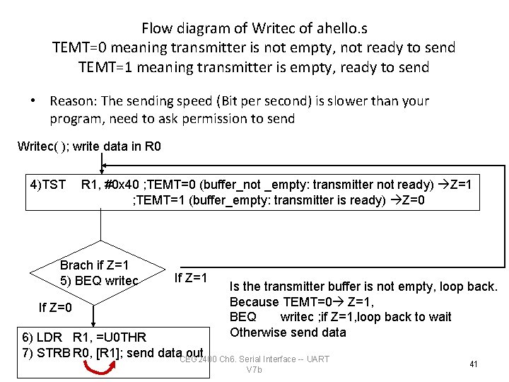
Flow diagram of Writec of ahello. s TEMT=0 meaning transmitter is not empty, not ready to send TEMT=1 meaning transmitter is empty, ready to send • Reason: The sending speed (Bit per second) is slower than your program, need to ask permission to send Writec( ); write data in R 0 4)TST R 1, #0 x 40 ; TEMT=0 (buffer_not _empty: transmitter not ready) Z=1 ; TEMT=1 (buffer_empty: transmitter is ready) Z=0 Brach if Z=1 5) BEQ writec If Z=0 If Z=1 Is the transmitter buffer is not empty, loop back. Because TEMT=0 Z=1, BEQ writec ; if Z=1, loop back to wait Otherwise send data 6) LDR R 1, =U 0 THR 7) STRB R 0, [R 1]; send data. CEG 2400 out Ch 6. Serial Interface -- UART V 7 b 41

Summary • Studied serial interface in ARM • Studied handshaking in interfacing CEG 2400 Ch 6. Serial Interface -- UART V 7 b 42

End CEG 2400 Ch 6. Serial Interface -- UART V 7 b 43