Chapter 4 UART Serial Port Programming 1 Serial

- Slides: 36

Chapter 4 UART Serial Port Programming 1

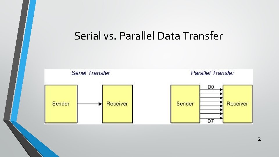
Serial vs. Parallel Data Transfer 2

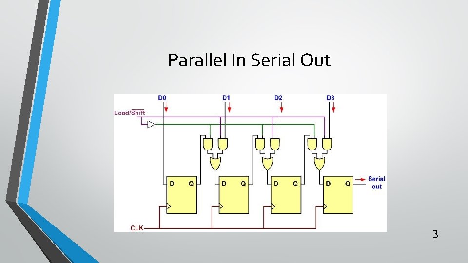
Parallel In Serial Out 3

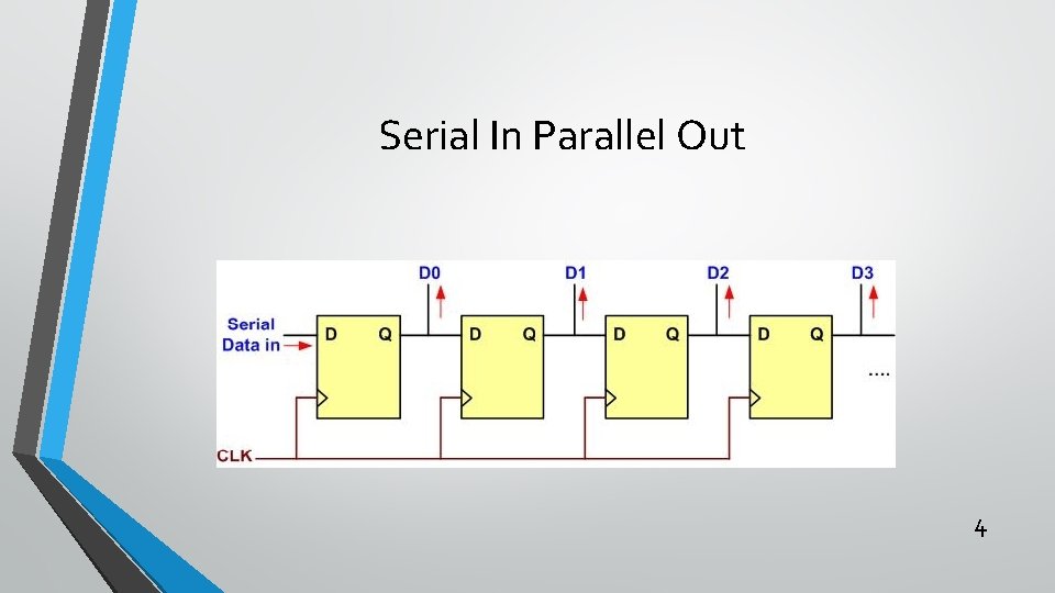
Serial In Parallel Out 4

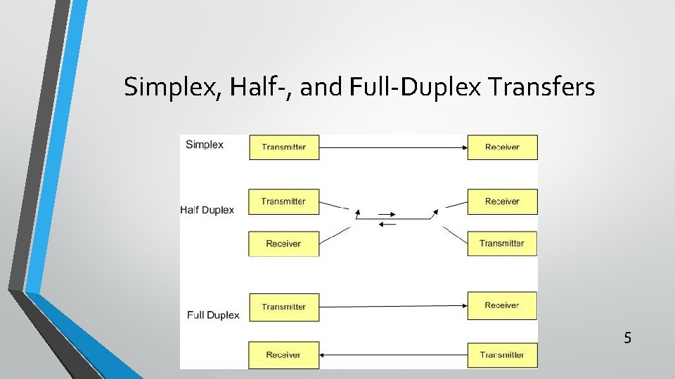
Simplex, Half-, and Full-Duplex Transfers 5

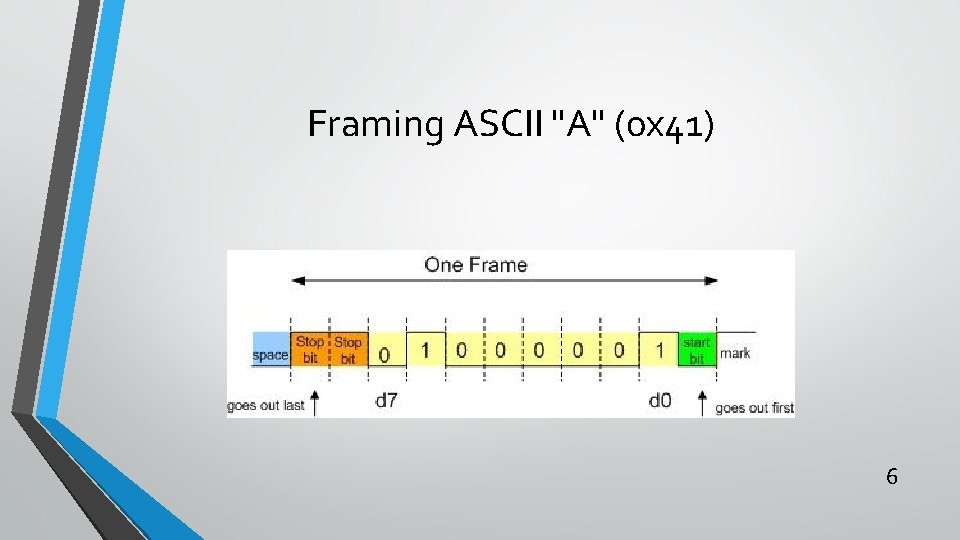
Framing ASCII "A" (0 x 41) 6

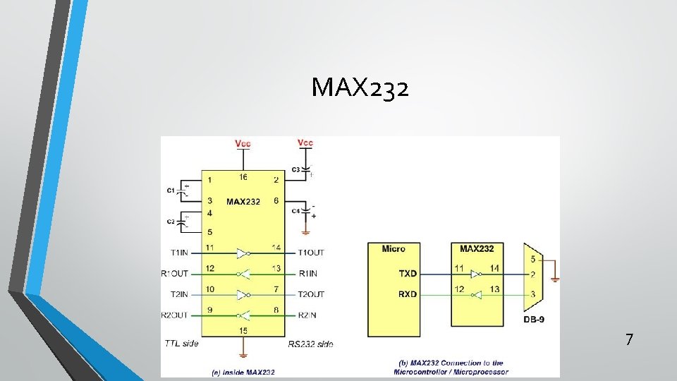
MAX 232 7

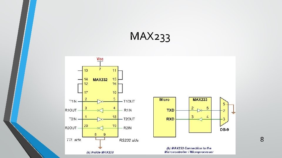
MAX 233 8

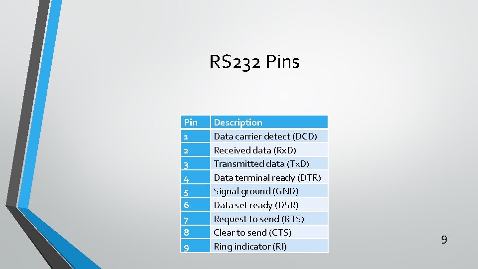
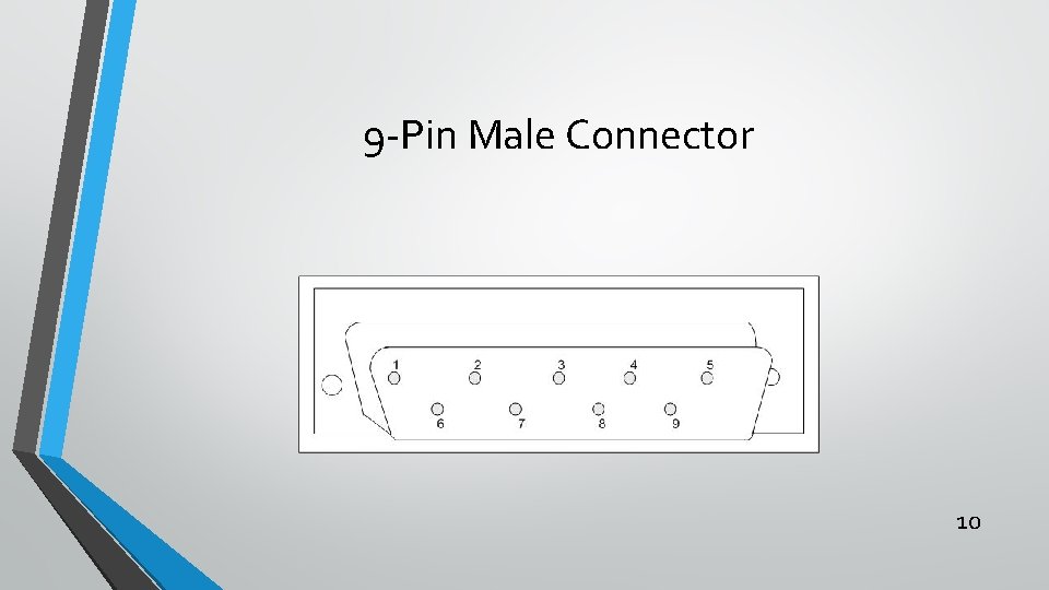
RS 232 Pins Pin 1 2 3 4 5 6 7 8 9 Description Data carrier detect (DCD) Received data (Rx. D) Transmitted data (Tx. D) Data terminal ready (DTR) Signal ground (GND) Data set ready (DSR) Request to send (RTS) Clear to send (CTS) Ring indicator (RI) 9

9 -Pin Male Connector 10

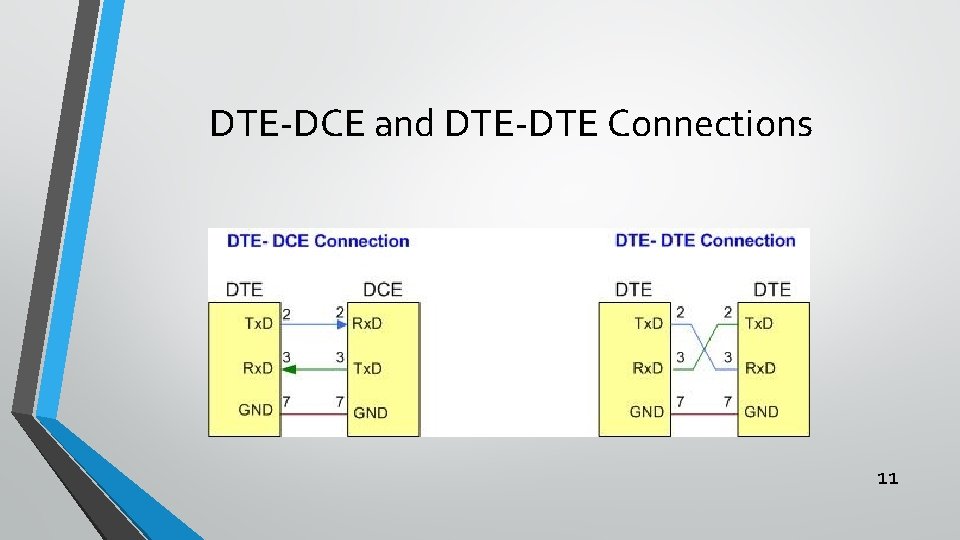
DTE-DCE and DTE-DTE Connections 11

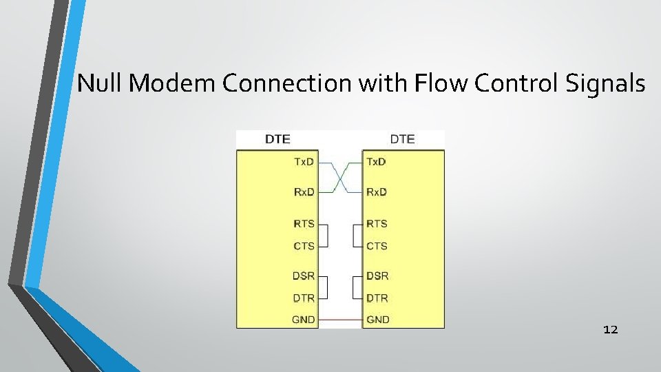
Null Modem Connection with Flow Control Signals 12

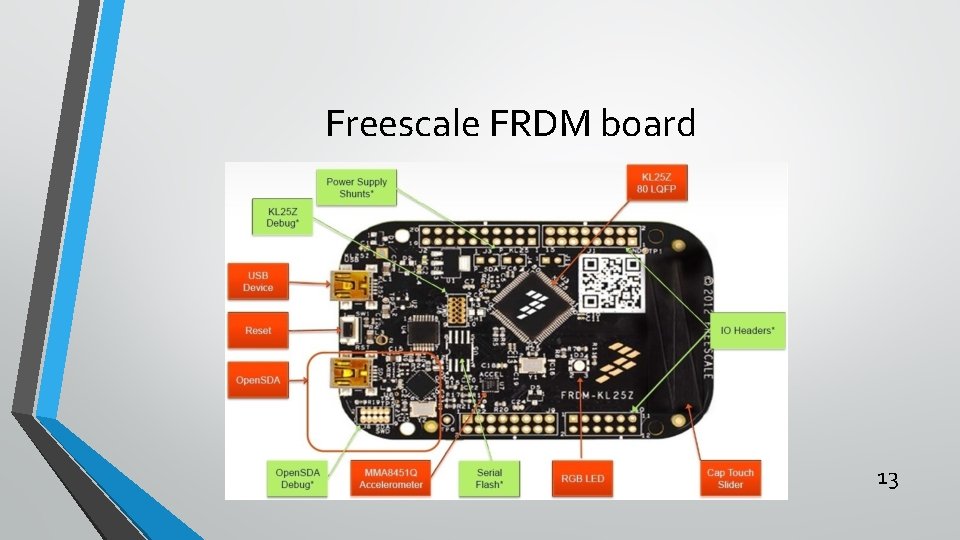
Freescale FRDM board 13

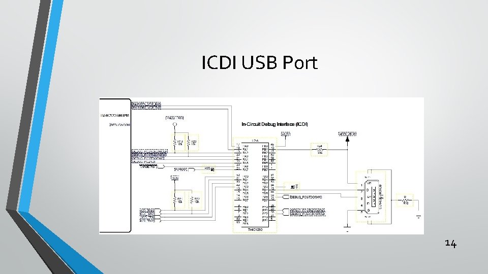
ICDI USB Port 14

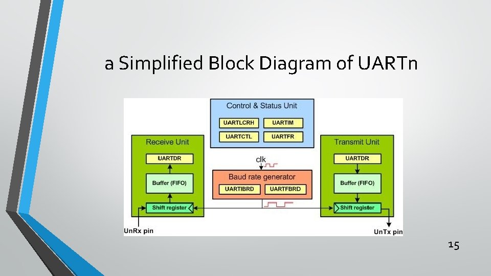
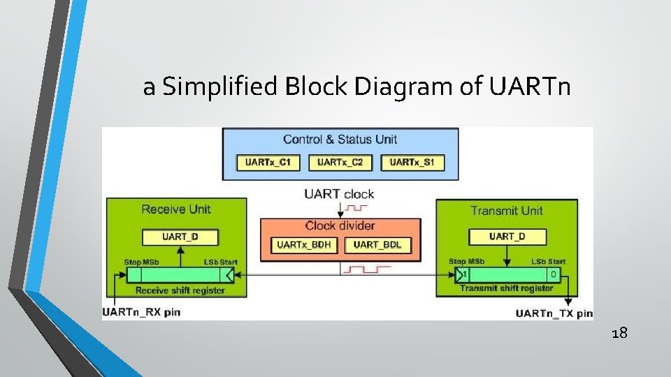
a Simplified Block Diagram of UARTn 15

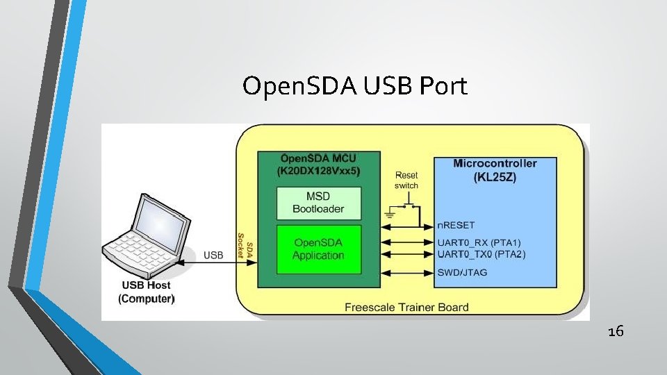
Open. SDA USB Port 16

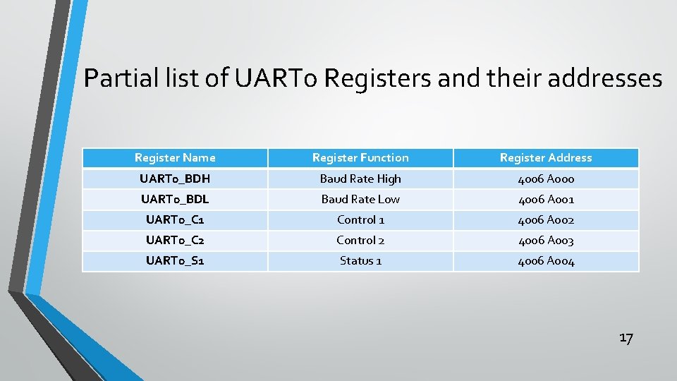
Partial list of UART 0 Registers and their addresses Register Name Register Function Register Address UART 0_BDH Baud Rate High 4006 A 000 UART 0_BDL Baud Rate Low 4006 A 001 UART 0_C 1 Control 1 4006 A 002 UART 0_C 2 Control 2 4006 A 003 UART 0_S 1 Status 1 4006 A 004 17

a Simplified Block Diagram of UARTn 18

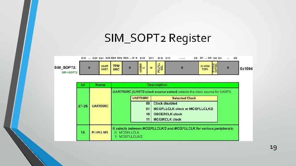
SIM_SOPT 2 Register 19

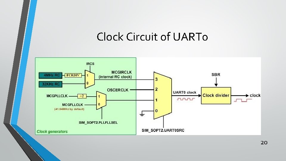
Clock Circuit of UART 0 20

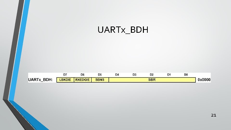
UARTx_BDH 21

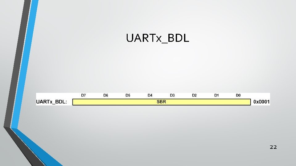
UARTx_BDL 22

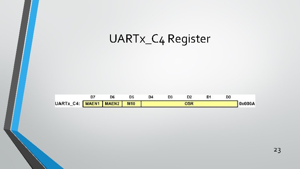
UARTx_C 4 Register 23

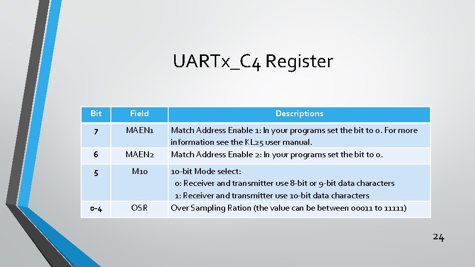
UARTx_C 4 Register Bit Field 7 MAEN 1 6 MAEN 2 5 M 10 0 -4 OSR Descriptions Match Address Enable 1: In your programs set the bit to 0. For more information see the KL 25 user manual. Match Address Enable 2: In your programs set the bit to 0. 10 -bit Mode select: 0: Receiver and transmitter use 8 -bit or 9 -bit data characters 1: Receiver and transmitter use 10 -bit data characters Over Sampling Ration (the value can be between 00011 to 11111) 24

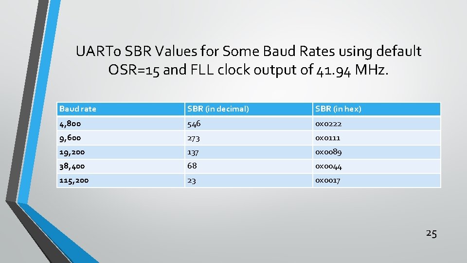
UART 0 SBR Values for Some Baud Rates using default OSR=15 and FLL clock output of 41. 94 MHz. Baud rate SBR (in decimal) SBR (in hex) 4, 800 546 0 x 0222 9, 600 273 0 x 0111 19, 200 137 0 x 0089 38, 400 68 0 x 0044 115, 200 23 0 x 0017 25

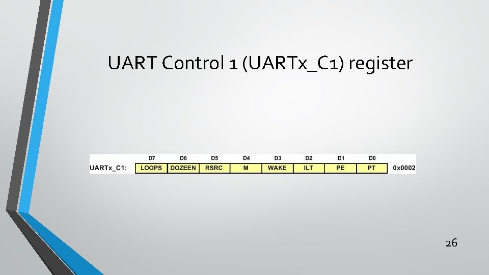
UART Control 1 (UARTx_C 1) register 26

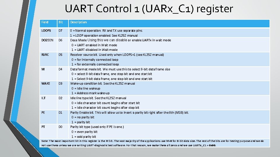
UART Control 1 (UARx_C 1) register Field Bit Description LOOPS D 7 DOZEEN D 6 RSRC D 5 M D 4 WAKE D 3 ILT D 2 PE D 1 PT D 0 0 = Normal operation. RX and TX use separate pins. 1 = LOOP operation enabled. See KL 25 Z manual Doze Mode Using this we can disable or enable UARTx in wait mode 0 = UART enabled in Wait mode 1 = UART disabled in Wait mode Receiver source bit. Used only when LOOPS=1 (see KL 25 Z manual) 0 = for internally connected loop 1 = for externally connected loop Data format mode bit. We must use this to select 8 -bit data frame size 0 = select 8 -bit data frame, one stop bit and one start bit 1 = Select 9 -bit data frame, one stop bit and one start bit Wake-up condition bit. See the KL 25 Z manual 0 = Idle line wakeup 1 = Address mark wake-up Idle line type bit. See the KL 25 Z manual 0 = Idle character bit count begins after start bit 1 = Idle character bit count begins after stop bit Parity Enable bit. This will allow us to insert a parity bit right after the 8 th (MSB) bit. 0 = no parity bit 1 = parity bit Parity bit type (used only if PE is one. ) 0 = even parity bit 1 = odd parity bit 27 Note: The most important bit in this register is the M bit. The vast majority of the applications use M=0 for 8 -bit data size. The rest of the bits are for testing purpose and we do not use them unless we are writing UART diagnostic test software. For that reason, we make them all zeros and we use UARTx_C 1 = 0 x 00.

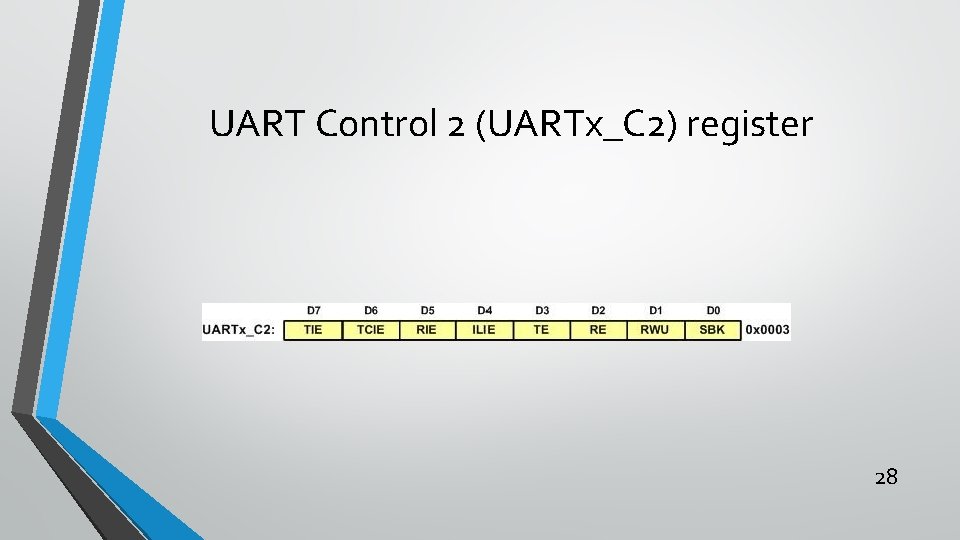
UART Control 2 (UARTx_C 2) register 28

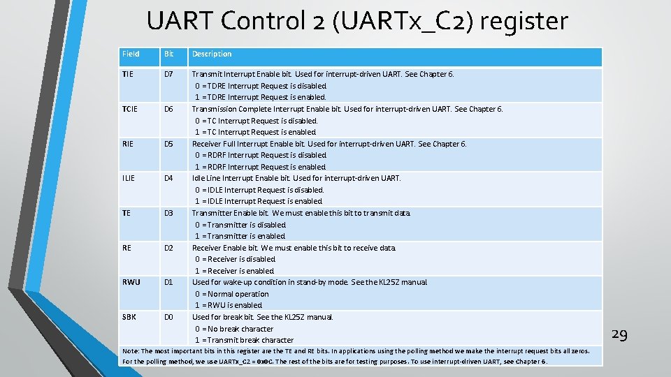
UART Control 2 (UARTx_C 2) register Field Bit Description TIE D 7 TCIE D 6 RIE D 5 ILIE D 4 TE D 3 RE D 2 RWU D 1 SBK D 0 Transmit Interrupt Enable bit. Used for interrupt-driven UART. See Chapter 6. 0 = TDRE Interrupt Request is disabled. 1 = TDRE Interrupt Request is enabled. Transmission Complete Interrupt Enable bit. Used for interrupt-driven UART. See Chapter 6. 0 = TC Interrupt Request is disabled. 1 = TC Interrupt Request is enabled. Receiver Full Interrupt Enable bit. Used for interrupt-driven UART. See Chapter 6. 0 = RDRF Interrupt Request is disabled. 1 = RDRF Interrupt Request is enabled. Idle Line Interrupt Enable bit. Used for interrupt-driven UART. 0 = IDLE Interrupt Request is disabled. 1 = IDLE Interrupt Request is enabled. Transmitter Enable bit. We must enable this bit to transmit data. 0 = Transmitter is disabled. 1 = Transmitter is enabled. Receiver Enable bit. We must enable this bit to receive data. 0 = Receiver is disabled. 1 = Receiver is enabled. Used for wake-up condition in stand-by mode. See the KL 25 Z manual. 0 = Normal operation 1 = RWU is enabled. Used for break bit. See the KL 25 Z manual. 0 = No break character 1 = Transmit break character Note: The most important bits in this register are the TE and RE bits. In applications using the polling method we make the interrupt request bits all zeros. For the polling method, we use UARTx_C 2 = 0 x 0 C. The rest of the bits are for testing purposes. To use interrupt-driven UART, see Chapter 6. 29

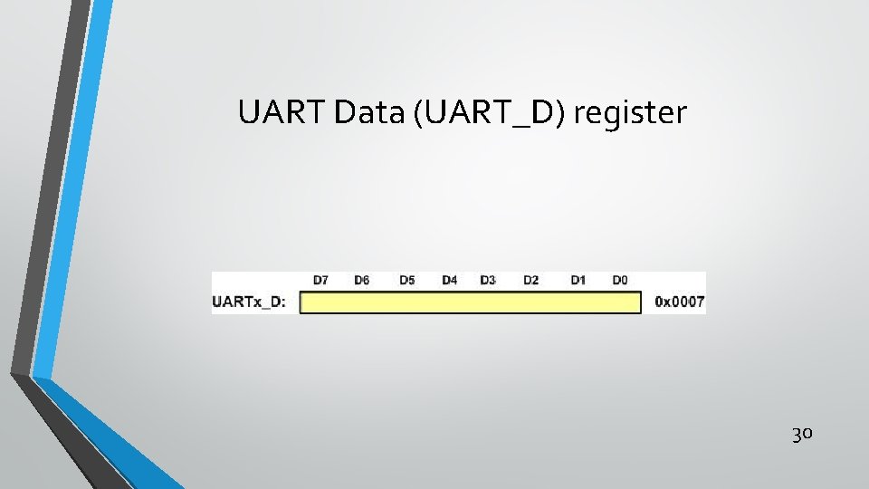
UART Data (UART_D) register 30

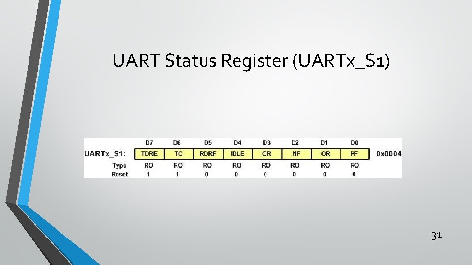
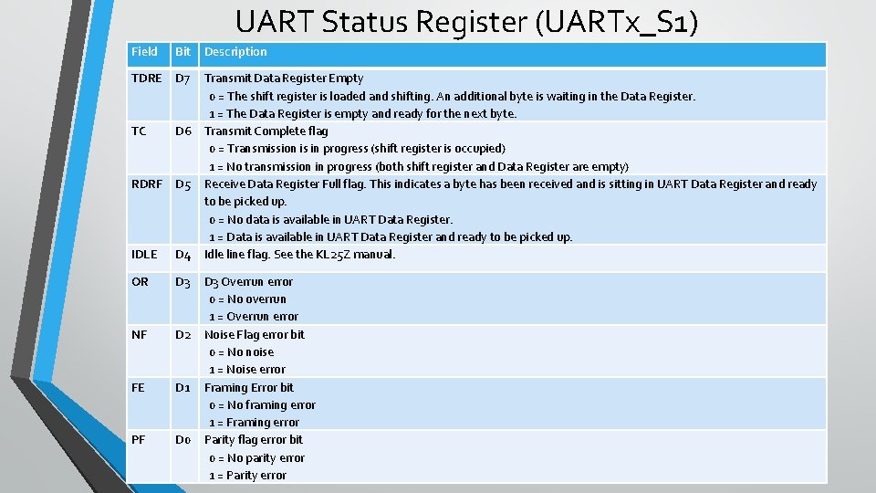
UART Status Register (UARTx_S 1) 31

UART Status Register (UARTx_S 1) Field Bit Description TDRE D 7 TC D 6 RDRF D 5 IDLE D 4 OR D 3 NF D 2 FE D 1 PF D 0 Transmit Data Register Empty 0 = The shift register is loaded and shifting. An additional byte is waiting in the Data Register. 1 = The Data Register is empty and ready for the next byte. Transmit Complete flag 0 = Transmission is in progress (shift register is occupied) 1 = No transmission in progress (both shift register and Data Register are empty) Receive Data Register Full flag. This indicates a byte has been received and is sitting in UART Data Register and ready to be picked up. 0 = No data is available in UART Data Register. 1 = Data is available in UART Data Register and ready to be picked up. Idle line flag. See the KL 25 Z manual. D 3 Overrun error 0 = No overrun 1 = Overrun error Noise Flag error bit 0 = No noise 1 = Noise error Framing Error bit 0 = No framing error 1 = Framing error Parity flag error bit 0 = No parity error 1 = Parity error 32

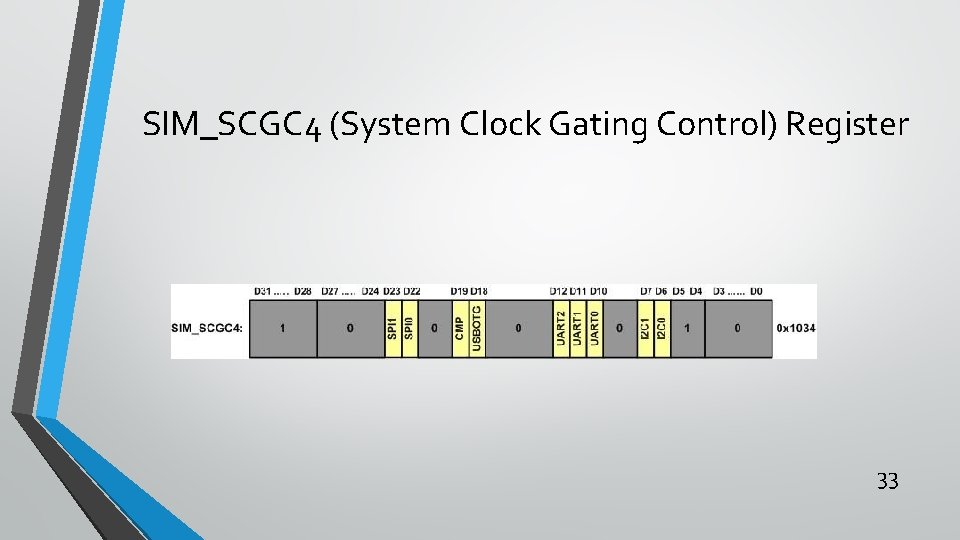
SIM_SCGC 4 (System Clock Gating Control) Register 33

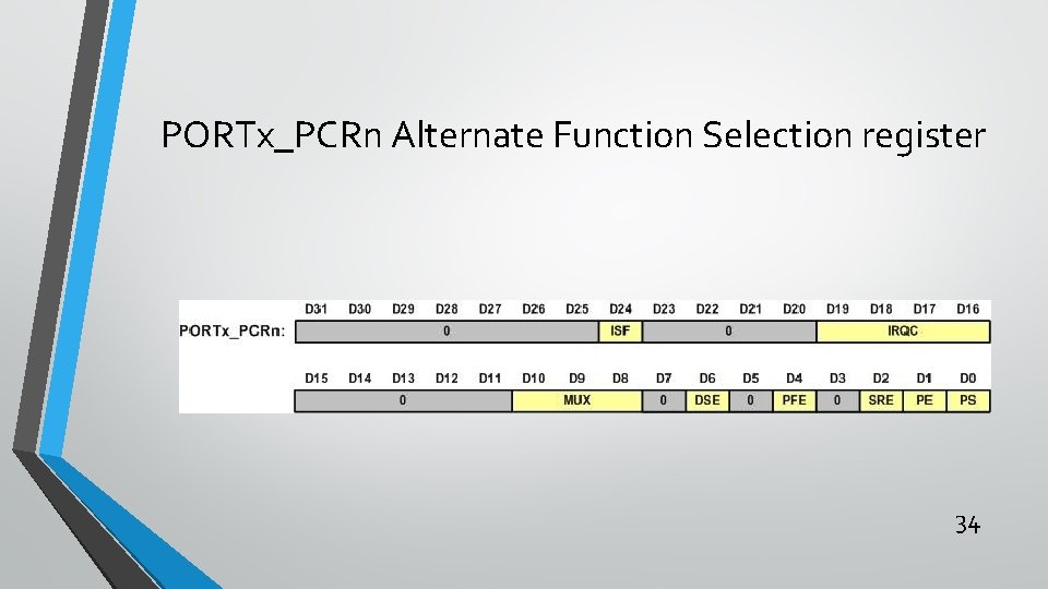
PORTx_PCRn Alternate Function Selection register 34

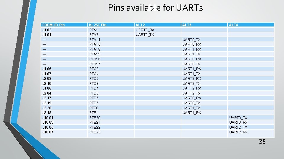
Pins available for UARTs FRDM I/O Pin J 1 02 J 1 04 ― ― ― J 1 05 J 1 07 J 2 08 J 2 10 J 1 06 J 2 04 J 2 17 J 2 19 J 2 20 J 2 18 J 10 01 J 10 03 J 10 05 J 10 07 KL 25 Z Pin PTA 1 PTA 2 PTA 14 PTA 15 PTA 18 PTA 19 PTB 16 PTB 17 PTC 3 PTC 4 PTD 2 PTD 3 PTD 4 PTD 5 PTD 6 PTD 7 PTE 0 PTE 1 PTE 20 PTE 21 PTE 22 PTE 23 ALT 2 UART 0_RX UART 0_TX ALT 3 ALT 4 UART 0_TX UART 0_RX UART 1_TX UART 0_RX UART 0_TX UART 1_RX UART 1_TX UART 2_RX UART 2_TX UART 0_RX UART 0_TX UART 1_RX UART 0_TX UART 0_RX UART 2_TX UART 2_RX 35

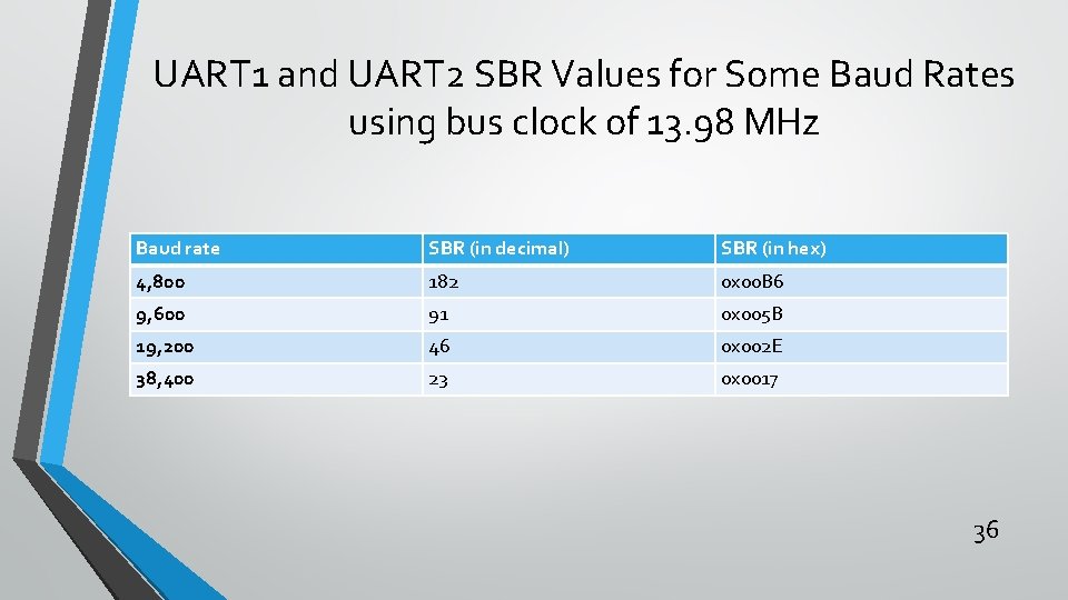
UART 1 and UART 2 SBR Values for Some Baud Rates using bus clock of 13. 98 MHz Baud rate SBR (in decimal) SBR (in hex) 4, 800 182 0 x 00 B 6 9, 600 91 0 x 005 B 19, 200 46 0 x 002 E 38, 400 23 0 x 0017 36