P 09311 Interface for Multipurpose Driver Data Acquisition
![UART System Signal Description CLK System Clock RST Asynchronous active-high reset. Din[7: 0] Eight-bits UART System Signal Description CLK System Clock RST Asynchronous active-high reset. Din[7: 0] Eight-bits](https://slidetodoc.com/presentation_image/3ce2549443a25a48665b7a1e2cb5c21d/image-24.jpg)
- Slides: 33

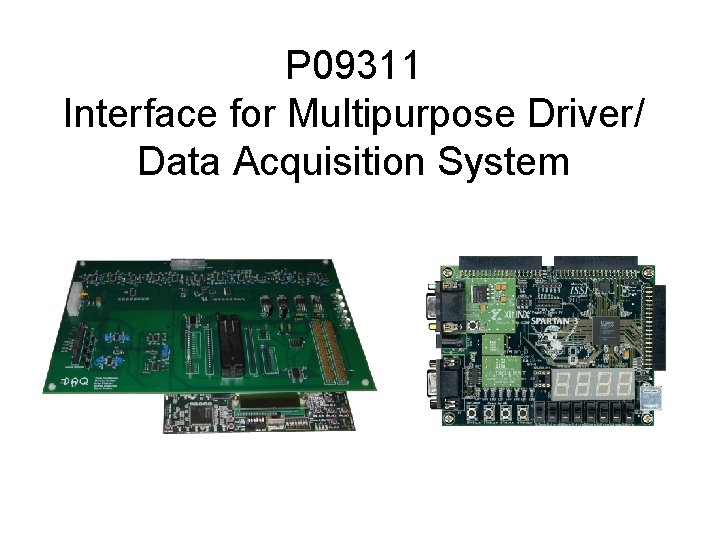
P 09311 Interface for Multipurpose Driver/ Data Acquisition System

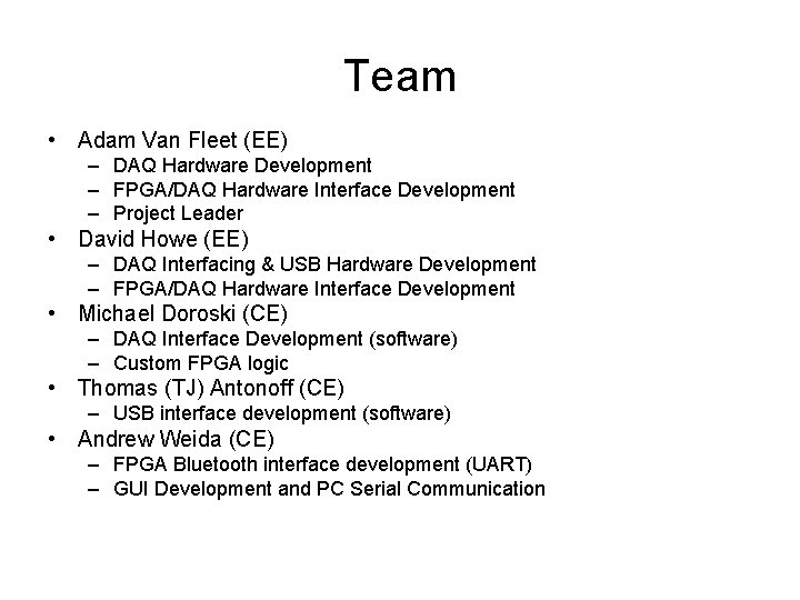
Team • Adam Van Fleet (EE) – DAQ Hardware Development – FPGA/DAQ Hardware Interface Development – Project Leader • David Howe (EE) – DAQ Interfacing & USB Hardware Development – FPGA/DAQ Hardware Interface Development • Michael Doroski (CE) – DAQ Interface Development (software) – Custom FPGA logic • Thomas (TJ) Antonoff (CE) – USB interface development (software) • Andrew Weida (CE) – FPGA Bluetooth interface development (UART) – GUI Development and PC Serial Communication

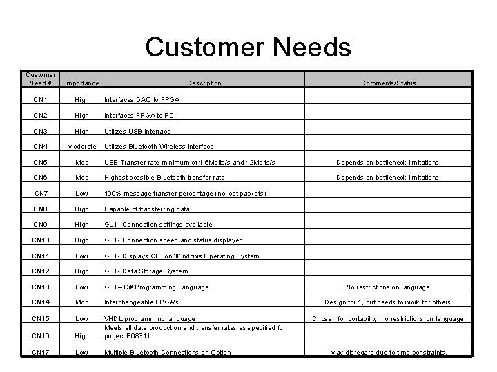
Customer Needs Customer Need # Importance CN 1 High Interfaces DAQ to FPGA CN 2 High Interfaces FPGA to PC CN 3 High Utilizes USB interface CN 4 Moderate Utilizes Bluetooth Wireless interface CN 5 Mod USB Transfer rate minimum of 1. 5 Mbits/s and 12 Mbits/s Depends on bottleneck limitations. CN 6 Mod Highest possible Bluetooth transfer rate Depends on bottleneck limitations. CN 7 Low 100% message transfer percentage (no lost packets) CN 8 High Capable of transferring data CN 9 High GUI - Connection settings available CN 10 High GUI - Connection speed and status displayed CN 11 Low GUI - Displays GUI on Windows Operating System CN 12 High GUI - Data Storage System CN 13 Low GUI – C# Programming Language CN 14 Mod Interchangeable FPGA's CN 15 Low CN 16 High VHDL programming language Meets all data production and transfer rates as specified for project P 08311 CN 17 Low Multiple Bluetooth Connections an Option Description Comments/Status No restrictions on language. Design for 1, but needs to work for others. Chosen for portability, no restrictions on language. May disregard due to time constraints.

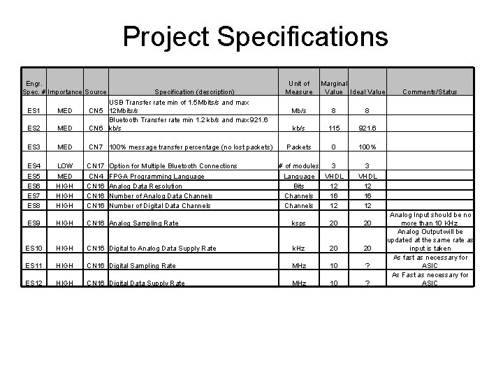
Project Specifications Engr. Spec. # Importance Source Specification (description) Unit of Measure Marginal Value Ideal Value ES 1 MED ES 2 MED USB Transfer rate min of 1. 5 Mbits/s and max CN 5 12 Mbits/s Bluetooth Transfer rate min 1. 2 kb/s and max 921. 6 CN 6 kb/s ES 3 MED CN 7 100% message transfer percentage (no lost packets) ES 4 ES 5 ES 6 ES 7 ES 8 LOW MED HIGH CN 17 CN 4 CN 16 ES 9 HIGH CN 16 Analog Sampling Rate ksps 20 20 ES 10 HIGH CN 16 Digital to Analog Data Supply Rate k. Hz 20 20 ES 11 HIGH CN 16 Digital Sampling Rate MHz 10 ? ES 12 HIGH CN 16 Digital Data Supply Rate MHz 10 ? Option for Multiple Bluetooth Connections FPGA Programming Language Analog Data Resolution Number of Analog Data Channels Number of Digital Data Channels Comments/Status Mb/s 8 8 kb/s 115 921. 6 Packets 0 100% 3 VHDL 12 16 12 # of modules 3 Language VHDL Bits 12 Channels 16 Channels 12 Analog Input should be no more than 10 KHz Analog Output will be updated at the same rate as input is taken As fast as necessary for ASIC As Fast as necessary for ASIC

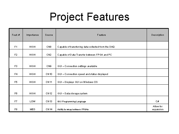
Project Features Feat. # Importance Source Feature Description F 1 HIGH CN 8 Capable of transferring data collected from the DAQ F 2 HIGH CN 2 Capable of Data Transfer between FPGA and PC F 3 HIGH CN 9 GUI – Connection settings available F 4 HIGH CN 10 GUI – Connection speed and status displayed F 5 HIGH CN 11 GUI – Displays GUI on Windows OS F 6 HIGH CN 12 GUI – Data storage system F 7 LOW CN 13 GUI Programming Language F 8 MED CN 14 Ability to swap between FPGAs C# Allow for expansion

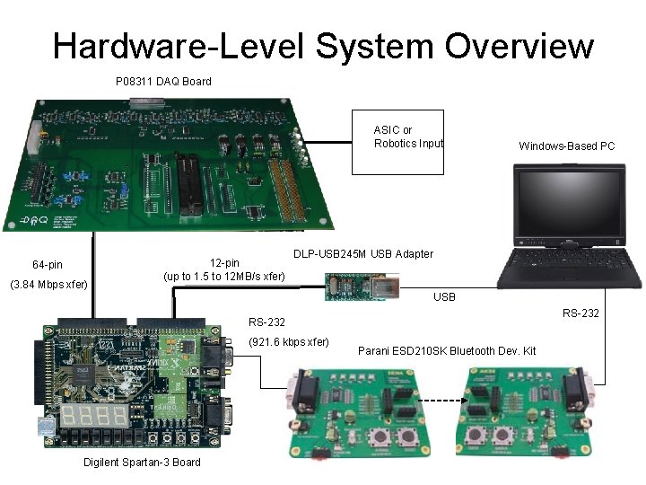
Hardware-Level System Overview P 08311 DAQ Board ASIC or Robotics Input 64 -pin (3. 84 Mbps xfer) 12 -pin (up to 1. 5 to 12 MB/s xfer) Windows-Based PC DLP-USB 245 M USB Adapter USB RS-232 (921. 6 kbps xfer) Digilent Spartan-3 Board Parani ESD 210 SK Bluetooth Dev. Kit

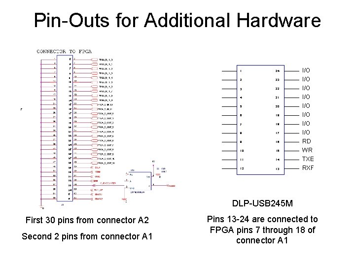
Pin-Outs for Additional Hardware 5 6 7 8 9 10 11 12 13 14 15 7 16 17 18 19 20 21 22 23 1 24 2 23 3 22 4 21 5 20 6 19 I/O I/O I/O 7 18 I/O 8 17 9 16 10 15 11 14 12 13 24 25 26 27 28 29 30 I/O RD WR TXE RXF 31 32 33 34 5 6 First 30 pins from connector A 2 Second 2 pins from connector A 1 DLP-USB 245 M Pins 13 -24 are connected to FPGA pins 7 through 18 of connector A 1

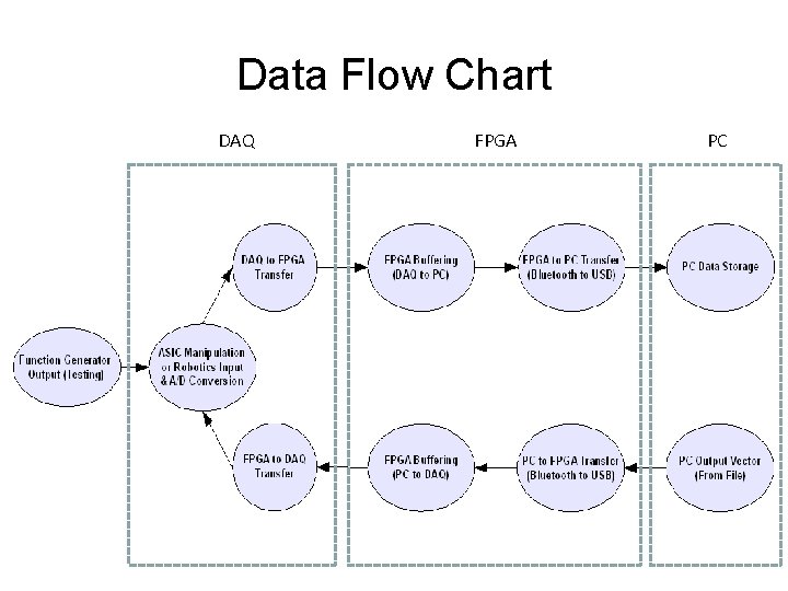
Data Flow Chart DAQ FPGA PC `

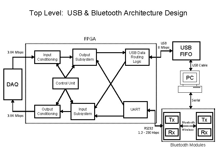
Top Level: USB & Bluetooth Architecture Design FPGA 3. 84 Mbps Input Conditioning Output Subsystem USB 8 Mbps USB FIFO USB Data Routing Logic USB Cable PC DAQ Control Unit Serial 3. 84 Mbps Output Conditioning Input Subsystem UART Tx RS 232 1. 2 - 230 kbps Rx Bluetooth Wireless Tx Rx Bluetooth Modules

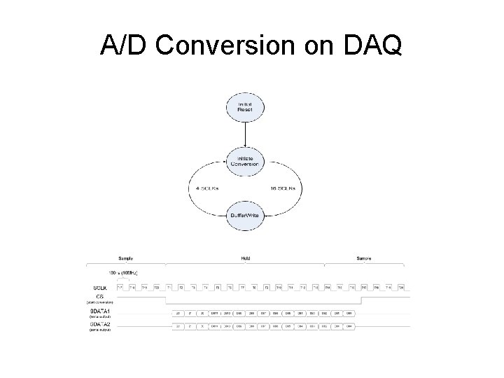
A/D Conversion on DAQ

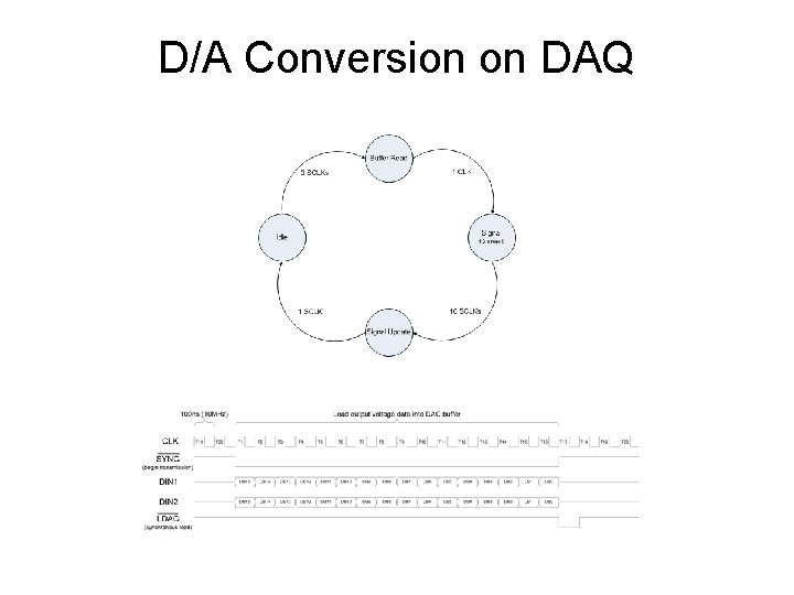
D/A Conversion on DAQ

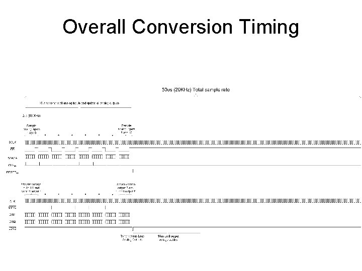
Overall Conversion Timing

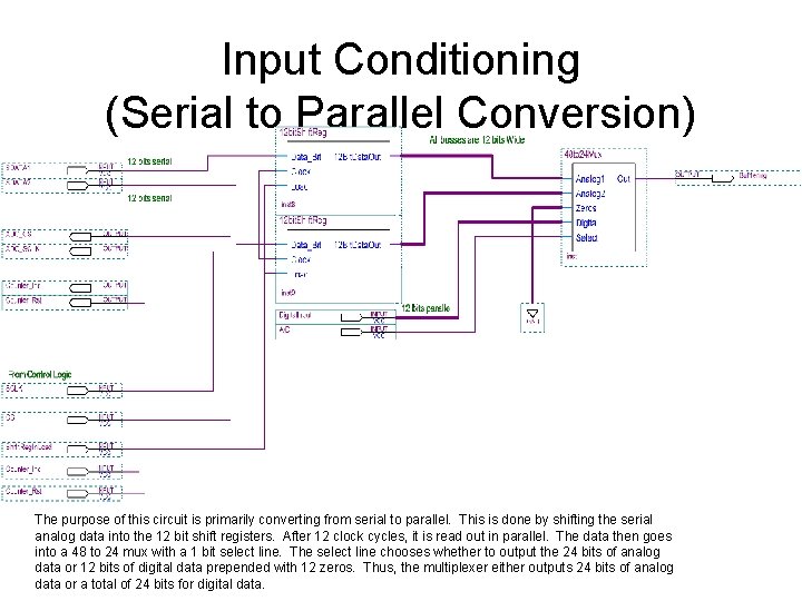
Input Conditioning (Serial to Parallel Conversion) The purpose of this circuit is primarily converting from serial to parallel. This is done by shifting the serial analog data into the 12 bit shift registers. After 12 clock cycles, it is read out in parallel. The data then goes into a 48 to 24 mux with a 1 bit select line. The select line chooses whether to output the 24 bits of analog data or 12 bits of digital data prepended with 12 zeros. Thus, the multiplexer either outputs 24 bits of analog data or a total of 24 bits for digital data.

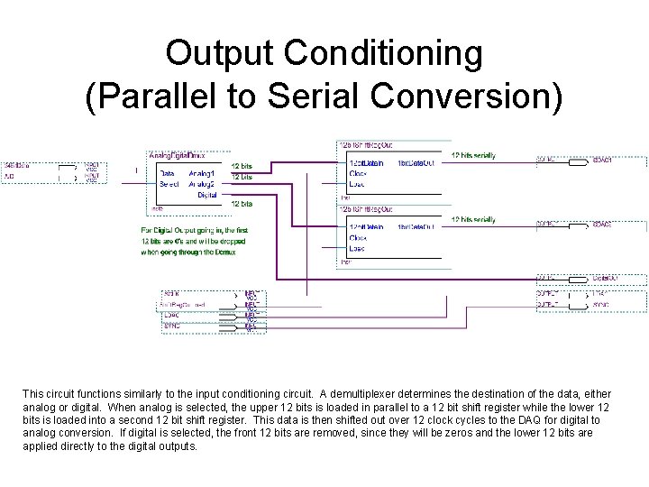
Output Conditioning (Parallel to Serial Conversion) This circuit functions similarly to the input conditioning circuit. A demultiplexer determines the destination of the data, either analog or digital. When analog is selected, the upper 12 bits is loaded in parallel to a 12 bit shift register while the lower 12 bits is loaded into a second 12 bit shift register. This data is then shifted out over 12 clock cycles to the DAQ for digital to analog conversion. If digital is selected, the front 12 bits are removed, since they will be zeros and the lower 12 bits are applied directly to the digital outputs.

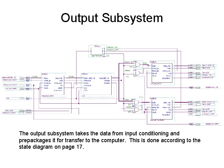
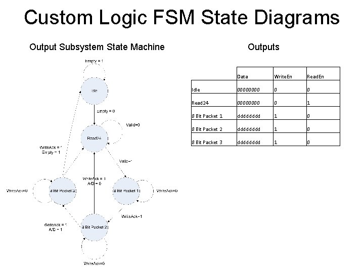
Output Subsystem The output subsystem takes the data from input conditioning and prepackages it for transfer to the computer. This is done according to the state diagram on page 17.

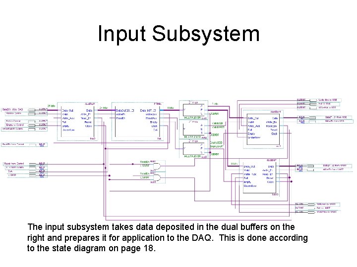
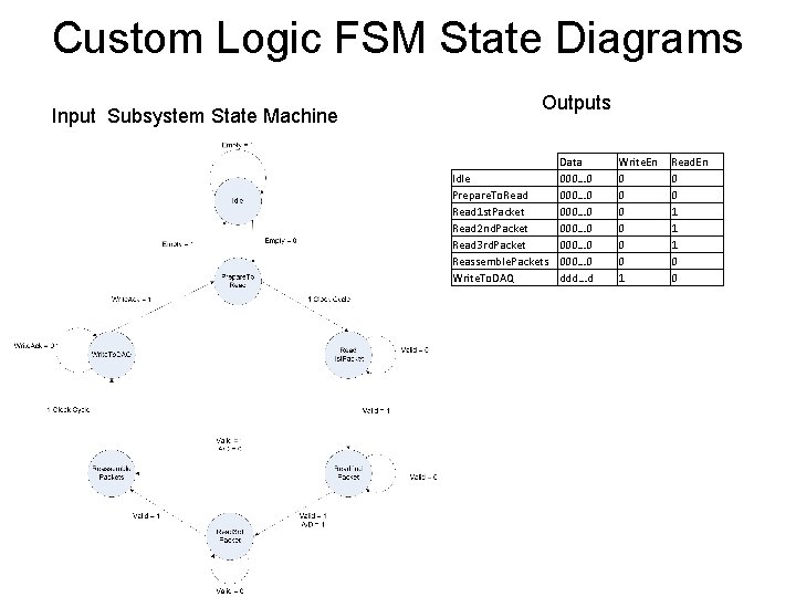
Input Subsystem The input subsystem takes data deposited in the dual buffers on the right and prepares it for application to the DAQ. This is done according to the state diagram on page 18.

Custom Logic FSM State Diagrams Output Subsystem State Machine Outputs Data Write. En Read. En Idle 0000 0 0 Read 24 0000 0 1 8 Bit Packet 1 dddd 1 0 8 Bit Packet 2 dddd 1 0 8 Bit Packet 3 dddd 1 0

Custom Logic FSM State Diagrams Input Subsystem State Machine Outputs Idle Prepare. To. Read 1 st. Packet Read 2 nd. Packet Read 3 rd. Packet Reassemble. Packets Write. To. DAQ Data 000… 0 000… 0 ddd…d Write. En 0 0 0 1 Read. En 0 0 1 1 1 0 0

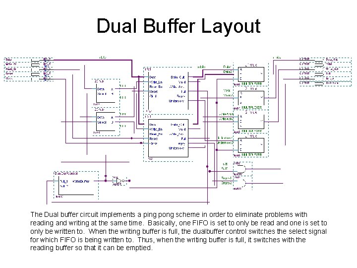
Dual Buffer Layout The Dual buffer circuit implements a ping pong scheme in order to eliminate problems with reading and writing at the same time. Basically, one FIFO is set to only be read and one is set to only be written to. When the writing buffer is full, the dualbuffer control switches the select signal for which FIFO is being written to. Thus, when the writing buffer is full, it switches with the reading buffer so that it can be emptied.

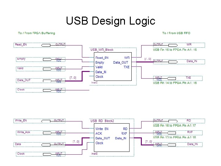
USB Design Logic

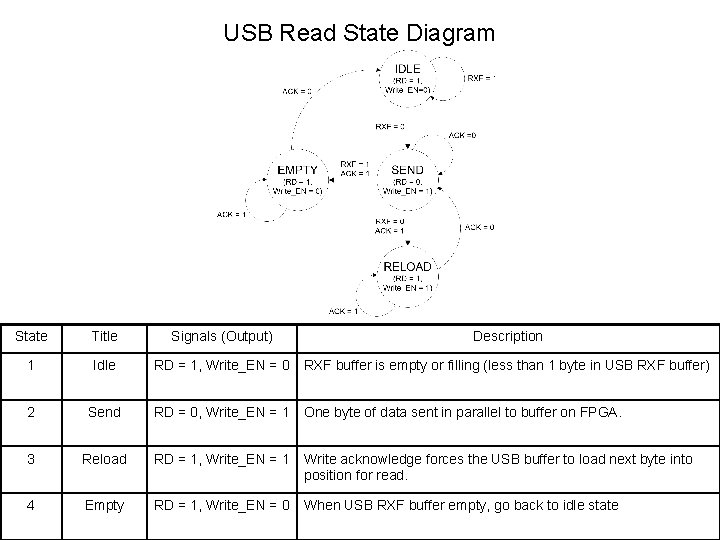
USB Read State Diagram State Title Signals (Output) Description 1 Idle RD = 1, Write_EN = 0 RXF buffer is empty or filling (less than 1 byte in USB RXF buffer) 2 Send RD = 0, Write_EN = 1 One byte of data sent in parallel to buffer on FPGA. 3 Reload RD = 1, Write_EN = 1 Write acknowledge forces the USB buffer to load next byte into position for read. 4 Empty RD = 1, Write_EN = 0 When USB RXF buffer empty, go back to idle state

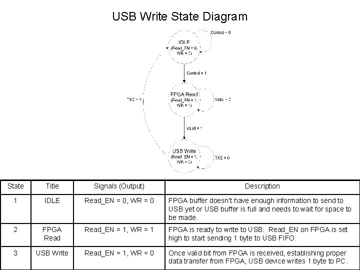
USB Write State Diagram State Title Signals (Output) Description 1 IDLE Read_EN = 0, WR = 0 FPGA buffer doesn’t have enough information to send to USB yet or USB buffer is full and needs to wait for space to be made. 2 FPGA Read_EN = 1, WR = 1 FPGA is ready to write to USB. Read_EN on FPGA is set high to start sending 1 byte to USB FIFO. 3 USB Write Read_EN = 1, WR = 0 Once valid bit from FPGA is received, establishing proper data transfer from FPGA, USB device writes 1 byte to PC.

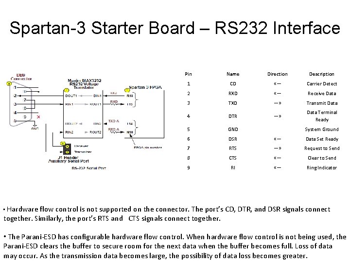
Spartan-3 Starter Board – RS 232 Interface Pin Name Direction Description 1 CD «— Carrier Detect 2 RXD «— Receive Data 3 TXD —» Transmit Data 4 DTR —» Data Terminal Ready 5 GND 6 DSR «— Data Set Ready 7 RTS —» Request to Send 8 CTS «— Clear to Send 9 RI «— Ring Indicator System Ground • Hardware flow control is not supported on the connector. The port’s CD, DTR, and DSR signals connect together. Similarly, the port’s RTS and CTS signals connect together. • The Parani-ESD has configurable hardware flow control. When hardware flow control is not being used, the Parani-ESD clears the buffer to secure room for the next data when the buffer becomes full. Loss of data may occur. As the transmission data becomes large, the possibility of data loss becomes greater.
![UART System Signal Description CLK System Clock RST Asynchronous activehigh reset Din7 0 Eightbits UART System Signal Description CLK System Clock RST Asynchronous active-high reset. Din[7: 0] Eight-bits](https://slidetodoc.com/presentation_image/3ce2549443a25a48665b7a1e2cb5c21d/image-24.jpg)
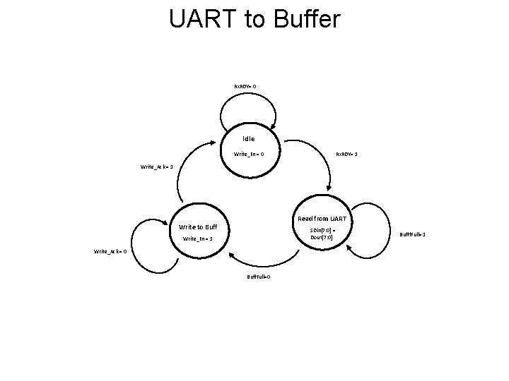
UART System Signal Description CLK System Clock RST Asynchronous active-high reset. Din[7: 0] Eight-bits Data From Buffer LD Load pulse to load Din in the Transmitter and start the transmission Rx RS 232 receive signal input. Is ’ 1’ when the line is idle. Tx RS 232 transmit signal output. Is ’ 1’ when the line is idle. Dout[7: 0] Data received. Rx. RDY A ‘ 1’ pulse (one system clock cycle long) indicates that a character is received and is available at Dout. Tx. Busy Indicates that the UART is busy sending data. Will ignore any LD request. SDin[7: 0] / SDout[7: 0] Data received from RS-232 Buff. Din[7: 0] / Buff. Dout[7: 0] Data From dual buffer, to be transmitted by UART Write. Buff / Read. Buff Control signal to write or read to/from Dual Buffer Buff. Full / Buff. Empty Indicates if Buffers are Full or Empty.

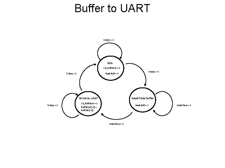
Buffer to UART Empty = 1 Idle LD_Buff. Dout = 0 Write to UART Tx. Busy = 1 Empty = 0 Read. Buff = 0 Tx. Busy = 1 Read from Buffer LD_Buff. Dout = 1 Buff. Dout[7: 0] = Buff. Din[7: 0] Read. Buff = 1 Underflow = 0 Underflow = 1

UART to Buffer Rx. RDY= 0 Idle Write_En = 0 Rx. RDY= 1 Write_Ack = 1 Read from UART Write to Buff SDin[7: 0] = Dout[7: 0] Write_En = 1 Write_Ack = 0 Buff. Full=0 Bufff. Full= 1

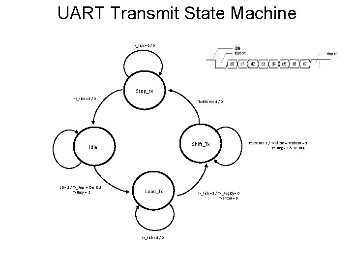
UART Transmit State Machine tx_tick = 0 / 0 Stop_tx tx_tick = 1 / 0 Tx. Bit. Cnt = 1 / 0 Shift_Tx Idle LD = 1 / Tx_Reg = Din & 1 Tx. Busy = 1 Load_Tx tx_tick = 1 / 0 tx_tick = 1 / Tx_Reg(0) = 0 Tx. Bit. Cnt = 9 Tx. Bit. Cnt > 1 / Tx. Bit. Cnt = Tx. Bit. Cnt – 1 Tx_Reg = 1 & Tx_Reg

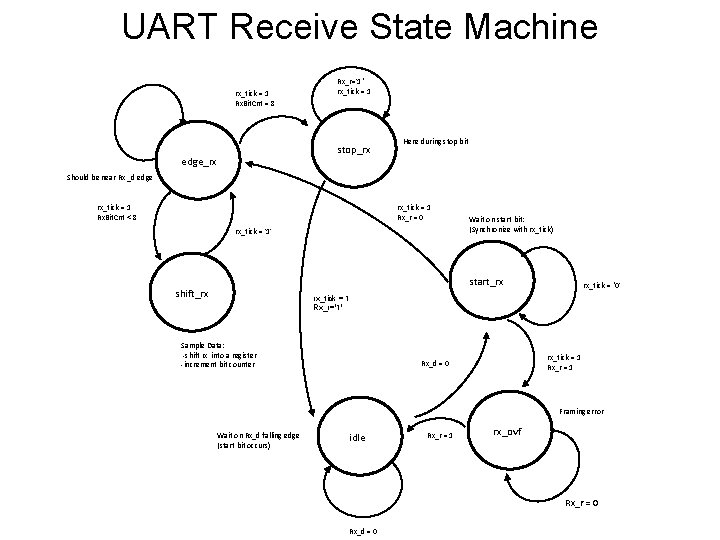
UART Receive State Machine rx_tick = 1 Rx. Bit. Cnt = 8 Rx_r='1‘ rx_tick = 1 stop_rx edge_rx Here during stop bit Should be near Rx _d edge rx_tick = 1 Rx. Bit. Cnt < 8 rx_tick = 1 Rx_r = 0 rx_tick = '1' Wait on start bit: (Synchronize with rx_tick) start_rx shift_rx rx_tick = ‘ 0' rx_tick = 1 Rx_r='1' Sample Data: -shift rx into a register -increment bit counter rx_tick = 1 Rx_r = 1 Rx_d = 0 Framing error Wait on Rx_d falling edge (start bit occurs) idle Rx_r = 1 rx_ovf Rx_r = 0 Rx_d = 0

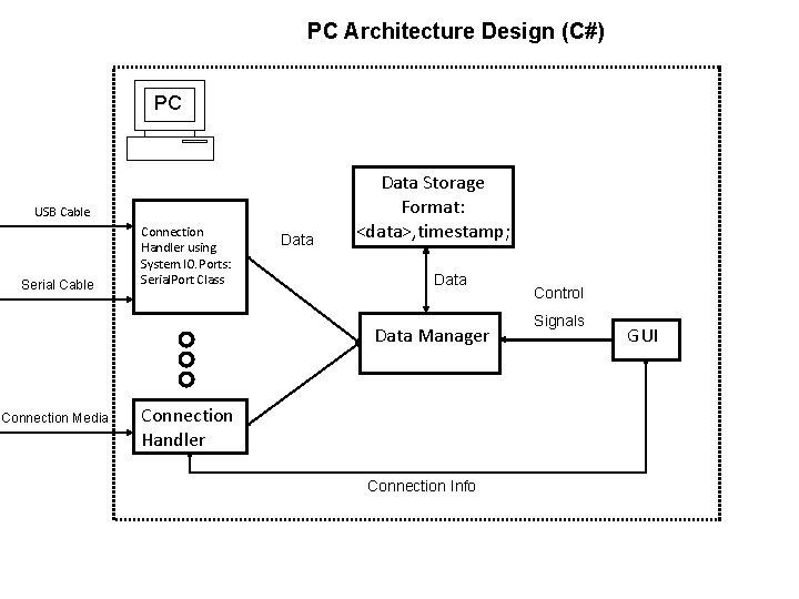
PC Architecture Design (C#) PC USB Cable Serial Cable Connection Handler using System. IO. Ports: Serial. Port Class Data Storage Format: <data>, timestamp; Data Manager Connection Media Connection Handler Connection Info Control Signals GUI

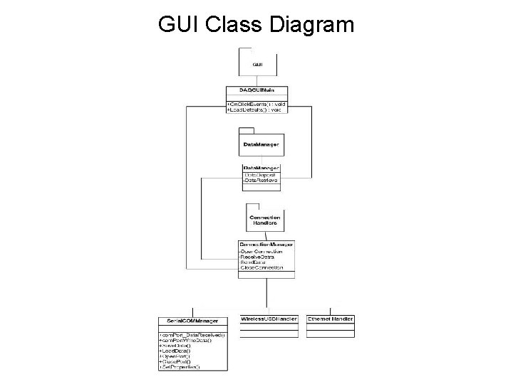
GUI Class Diagram

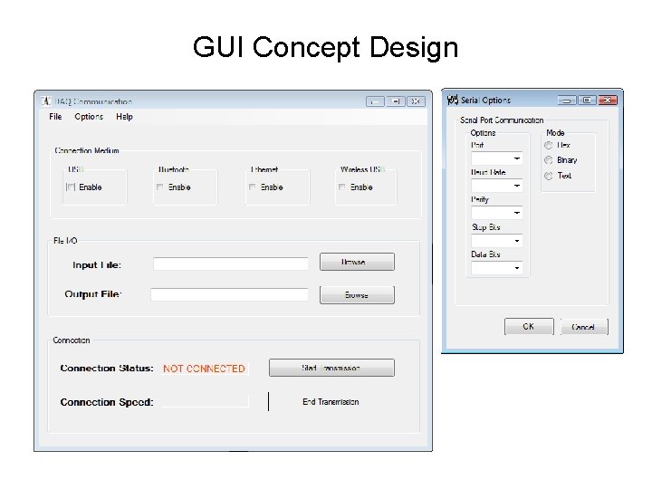
GUI Concept Design

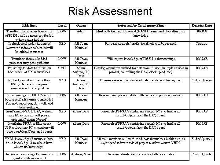
Risk Assessment Risk Item Level Owner Status and/or Contingency Plans Decision Date Transfer of knowledge from work of P 08311 will be necessary for full system understanding Technological understanding of hardware / software to be used will be critical to success LOW Adam Meet with Andrew Fitzgerald (P 08311 Team Lead) to gather prior knowledge 10/3/08 MED All Team Members Personal research / professional help will be required Ongoing Transition from embedded processor may pose problems LOW All Team Members Will require knowledge of P 08311’s shortcomings 10/17/08 Possibility for data transmission bottlenecks at FPGA interfaces CRIT Develop alternative method for data transmission (multiple devices in parallel, controlling the DAQ clock speed, etc. ) 10/17/08 No background in Bluetooth or USB; interface will require considerable time to produce MED Adam, Andrew, TJ, Dave Extensive research of modes of data transfer will be required End of Quarter Shortcomings of P 08311’s work (Compact flash memory, embedded Power. PC processor, etc. ) will need to be evaluated Interfacing FPGA to DAQ without any I/O expansion will pose a problem (Spartan-3 board) Interfacing FPGA to Bluetooth / USB without any I/O expansion will pose a problem (Spartan-3 board) LOW All Team Members Research into previous data bottlenecks and possible solutions 10/17/08 MED Adam, Dave Research of FPGA’s containing enough I/O’s to handle all inputs/outputs from the DAQ board 10/17/08 LOW Adam, Dave Research of FPGA’s containing enough I/O’s to handle all inputs/outputs from the DAQ board 10/17/08 VHDL knowledge (3 members have basic knowledge, 2 members have almost no knowledge) MED All Team Members All team members will need to educate themselves in this area, as majority of software side of project revolves around VHDL End of Quarter Accurate monitoring of connection speed and status via GUI LOW Andrew, Mike Decrease refresh rate to allow for better calculation End of Quarter

Appendix Spartan-3 Board Reference Material http: //www. digilentinc. com/Products/Detail. cfm? Prod=S 3 BOARD&Nav 1=Products&N av 2=Programmable DLP-USB 245 M USB Adapter http: //www. dlpdesign. com/usb 245. shtml Parani ESD 210 SK Bluetooth Dev. Kit http: //www. rfphone. com/files/ESD 110. pdf Digital to Analog Converter http: //www. analog. com/static/imported-files/data_sheets/AD 5308_5318_5328. pdf Analog to Digital Converter http: //cache. national. com/ds/DC/ADC 121 S 101. pdf