EUSART Serial Communication UART Universal Asynchronous ReceiverTransmitter Receive

 Transmit: Convert")


: Cascade of flip-flops • Data written serially by shifting.")
 reverses process. All bits written to register")


 & BRG 16 (BAUDCTL) • TXEN = 1:")
 & BRG 16 (BAUDCTL) • CREN = 1:")


 determines address size. • ADDEN = 1 allows")


- Slides: 19
EUSART Serial Communication
UART • • Universal Asynchronous Receiver/Transmitter Receive: Convert serial to parallel (SIPO) Transmit: Convert parallel to serial (PISO) Asynchronous: No clock; bytes sent in chunks. – Start (0) and stop (1) signal for each byte
EUSART • Enhanced Universal Synchronous / Asynchronous Receiver/Transmitter • Synchronous: Constant stream of data matched with clock signal. – More efficient, no start/stop framing required. • Enhanced: Advanced features – Sleep mode/auto-wake – Calculate incoming baud rate – Error Detection • Full-duplex asynchronous, Half-duplex synchronous • 8 or 9 bit character length
Flip-Flop • Flip-flops store a single bit of data. • SR NOR latch: Simplest type of flip flop.
D Flip-Flop • Similar function, but uses clock to feed Data signal to Q in time with clock cycle.
Receive • Shift Register (RSR): Cascade of flip-flops • Data written serially by shifting. • Upon filling register, all bits read simultaneously on clock cycle.
Transmit • • Altered shift register (TSR) reverses process. All bits written to register simultaneously. Bits shift to next flip-flop on cycles. Last bit feeds output.
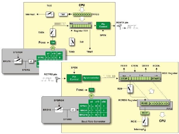
Registers • TXSTA & RCSTA: Status registers. – Set modes. • TSR & RSR: Shift registers. – Not directly accessible. • TXREG & RCREG: Container for transmitted data. • BAUDCTL: 8 -bit Baud Rate Control Register. • SPBRG & SPBRGH: 16 -bit Baud Rate Generator.
TXSTA – Transmit Status Register • CSRC - Clock Source Select bit - determines clock source. It is used only in synchronous mode. – – • +TX 9 - 9 -bit Transmit Enable bit – – • 1 - EUSART operates at high speed 0 - EUSART operates at low speed. TRMT - Transmit Shift Register Status bit – – • 1 - Sending Break character is enabled 0 - Break character transmission is completed. *BRGH - High Baud Rate Select bit determines baud rate in asynchronous mode. It does not affect EUSART in synchronous mode. – – • 1 - EUSART operates in synchronous mode 0 - EUSART operates in asynchronous mode. SENDB - Send Break Character bit is only used in asynchronous mode and only in case it is required to observe LIN bus standard. – – • *1 - Transmission enabled 0 - Transmission disabled. *SYNC - EUSART Mode Select bit – – • 1 - 9 -bit data transmission via EUSART system 0 - 8 -bit data transmission via EUSART system. *TXEN - Transmit Enable bit – – • 1 - Master mode. Clock is generated internally from Baud Rate Generator 0 - Slave mode. Clock is generated from external source. 1 - TSR register is empty 0 - TSR register is full. TX 9 D - Ninth bit of Transmit Data can be used as address or parity bit.
• RCSTA – Receive Status Register *SPEN - Serial Port Enable bit – – • +RX 9 - 9 -bit Receive Enable bit – – • 1 - Receiving 9 -bit data via EUSART system 0 - Receiving 8 -bit data via EUSART system. SREN - Single Receive Enable bit is used only in synchronous mode when the microcontroller operates as master. – – • *1 - Serial port enabled. RX/DT and TX/CK pins are automatically configured as input and output respectively 0 - Serial port disabled. 1 - Single receive enabled 0 - Single receive disable. *CREN - Continuous Receive Enable bit acts differently depending on EUSART mode. – Asynchronous mode: • • – Synchronous mode: • • • 1 - On receive, Framing Error is detected 0 - No framing error. ~OERR - Overrun Error bit. – – • 1 - Enables address detection on 9 -bit data receive 0 - Disables address detection. The ninth bit can be used as parity bit. ~FERR - Framing Error bit – – • *1 - Enables continuous receive until the CREN bit is cleared 0 - Disables continuous receive. +ADDEN - Address Detect Enable bit is only used in address detect mode. – – • *1 - Receiver enabled 0 - Receiver disabled. 1 - On receive, Overrun Error is detected 0 - No overrun error. RX 9 D - Ninth bit of Received Data can be used as address or parity bit.
BAUDCTL – Baud Rate Control Register • *Bit 7: ABDOVF — Flag bit indicates time of overflow; sets rate. – 1 - Auto-baud timer overflowed – 0 - Auto-baud timer did not overflow. • Bit 6: RCIDL — Idle/Sleep; only used in asynchronous mode. – 1 - Receiver is idle – 0 - START bit has been received and receiving is in progress. • Bit 4: SCKP – Synchronous: indicate which Idle state is used for the data Clock (CK) • 1 - Synchronization on rising edge of the clock • 0 - Synchronization on falling edge of the clock. – Asynchronous: indicate transmit polarity. • 1 - Transmit inverted data to the RC 6/TX/CK pin • 0 - Transmit non-inverted data to the same pin. • *Bit 3: BRG 16 — Enable 16 -bit – 1 – Enable 16 -bit (disables BAUDCTL from setting rate). – 0 – Disable 16 -bit mode. • Bit 1: WUE — Auto-wake/Interrupt – 1 - Receiver waits for a falling edge on the RC 7/RX/DT pin to wake from sleep. – 0 - Receiver operates normally. • Bit 0: ABDEN — Reset Baud – auto-baud recalculation on next character (async only) – 1 - Auto-baud detect mode is enabled. Bit is automatically cleared on baud rate detect. – 0 - Auto-baud detect mode is disabled.
Transmitter • Set Baud: BRGH (TXSTA) & BRG 16 (BAUDCTL) • TXEN = 1: Enable transmitter (TXSTA) • SPEN = 1: Enable Serial Port (RCSTA) – TX/CK pin is output • SYNC: Synchronous-1 or Asynchronous-0 (TXSTA) • TXREG: Write data to be sent here. • TSR: Data automatically transferred to TSR shift register from which it is serialized and output. • TXREG is cleared and awaits new data to repeat transmission.
Receiver • Set Baud: BRGH (TXSTA) & BRG 16 (BAUDCTL) • CREN = 1: Enable receiver (RCSTA) • SPEN = 1: Enable Serial Port (RCSTA) – Input to RX/DT pin • SYNC: Synchronous-1 or Asynchronous-0 (TXSTA) • RX/DT serial pin data sent to RSR shift register. • RCREG: 8 or 9 -bit data from RSR automatically transferred here. – Input data will be readable from RCREG register.
TX/RC Interrupts • Interrupt represents each successive byte. • Enable TXIE or RCIE to enable interrupt. • Transmit – When TXREG is empty, TXIF flag is set. – Flag Interrupt: Send to TXREG – TXIF is reset until TXREG is re-emptied. • Receive – Upon filling RCREG, RCIF flag is set. – Flag Interrupt: Read RCREG – RCIF flag is reset until RCREG is re-filled.
Example Code • Utilizing data received by EUSART. • http: //pastebin. com/W 1 c. P 6 bh 8 – Interrupt Routine • If RCIF flag is set, read EUSART (RCREG). • Flag code when read. – Main function: • Enable interrupt. • Endless loop. If flagged, read new data and place in array.
Address Detection • ADDEN bit (RCSTA) determines address size. • ADDEN = 1 allows 9 -bit, excludes 8 -bit • ADDEN = 0 disables address detection
Errors • Framing Error: In asynchronous mode – Stop bit not received at expected time. • Enables FERR bit (RCSTA). – Interrupt not necessarily generated, simply informs of possibly incorrect data. – FERR is cleared by once data is read. • Overrun Error – RCREG is FIFO and can hold no more than two bytes. – Third byte while RCREG is still full • Enables OERR bit (RCSTA). – No more data received until OERR is manually cleared (clear CREN). • Manual clearing of SPEN (RCSTA) will reset entire EUSART.
Reference • http: //ww 1. microchip. com/downloads/en/Ap p. Notes/00944 A. pdf • http: //www. mikroe. com/chapters/view/7/cha pter-6 -serial-communication-modules/