Simulation Synthesis of UART HD6402 using VHDL Presented
![Simulation & Synthesis of UART HD-6402 using VHDL Presented by [02 -384] Deepak Patel Simulation & Synthesis of UART HD-6402 using VHDL Presented by [02 -384] Deepak Patel](https://slidetodoc.com/presentation_image/5f9bd228b7756cbcebda609a22a0cad0/image-1.jpg)







- Slides: 25
![Simulation Synthesis of UART HD6402 using VHDL Presented by 02 384 Deepak Patel Simulation & Synthesis of UART HD-6402 using VHDL Presented by [02 -384] Deepak Patel](https://slidetodoc.com/presentation_image/5f9bd228b7756cbcebda609a22a0cad0/image-1.jpg)
Simulation & Synthesis of UART HD-6402 using VHDL Presented by [02 -384] Deepak Patel

Scope of our Project

VLSI and its Emergence

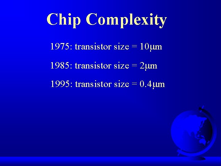
Chip Complexity 1975: transistor size = 10 m 1985: transistor size = 2 m 1995: transistor size = 0. 4 m

Introduction to VHDL

Design Process

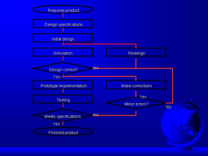
Required product Design specifications Initial design Simulation Design correct? Redesign No Yes Prototype implementation Make corrections Yes Testing Meets specifications? Yes Finished product Minor errors? No No

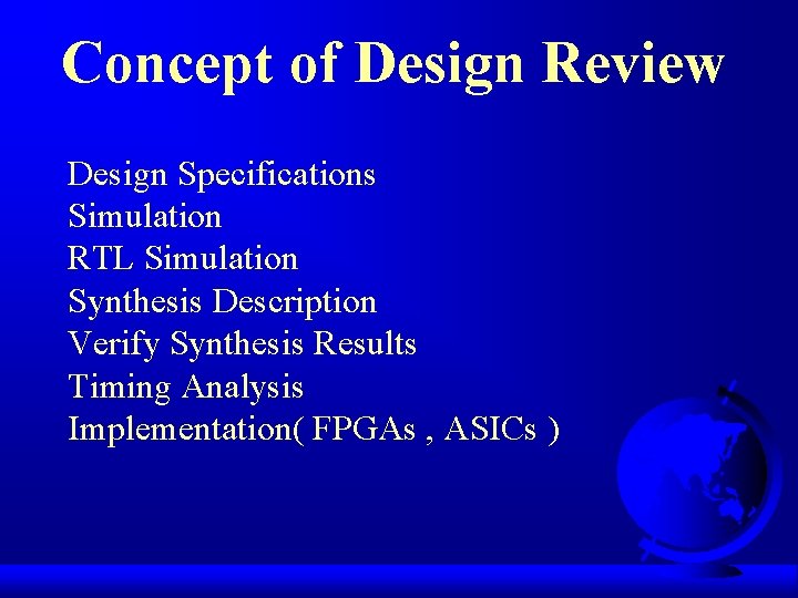
Concept of Design Review Design Specifications Simulation RTL Simulation Synthesis Description Verify Synthesis Results Timing Analysis Implementation( FPGAs , ASICs )

UART Basics for our project

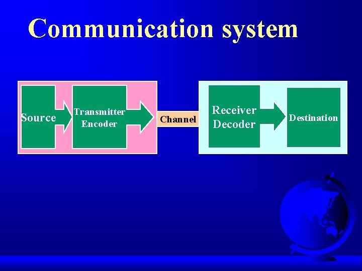
Communication system Source Transmitter Encoder Channel Receiver Decoder Destination

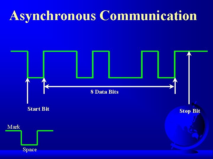
Asynchronous Communication 8 Data Bits Start Bit Mark Space Stop Bit

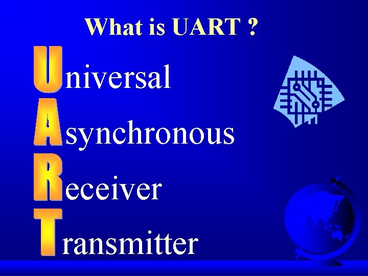
What is UART ? niversal synchronous eceiver ransmitter

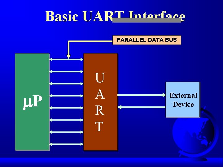
Basic UART Interface PARALLEL DATA BUS m. P U A R T External Device

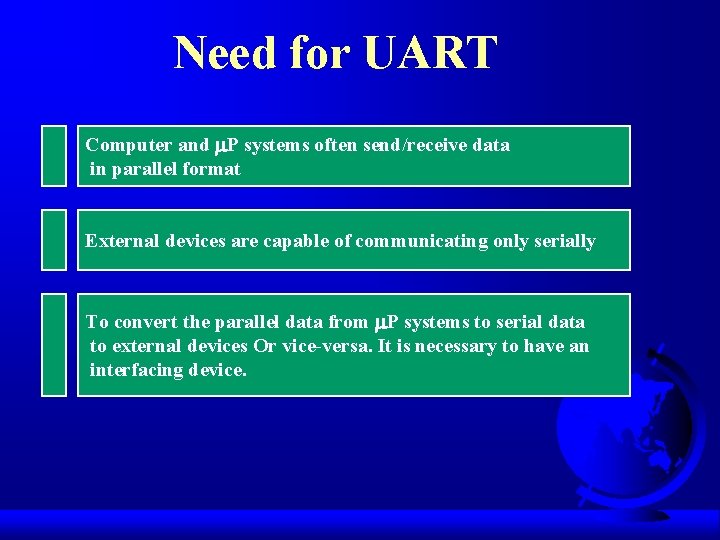
Need for UART Computer and m. P systems often send/receive data in parallel format External devices are capable of communicating only serially To convert the parallel data from m. P systems to serial data to external devices Or vice-versa. It is necessary to have an interfacing device.

Block Diagram of UART

Block Diagram of UART

Control Word

Advantages of Implementing UART using VHDL

How Stuff works ? ? ?

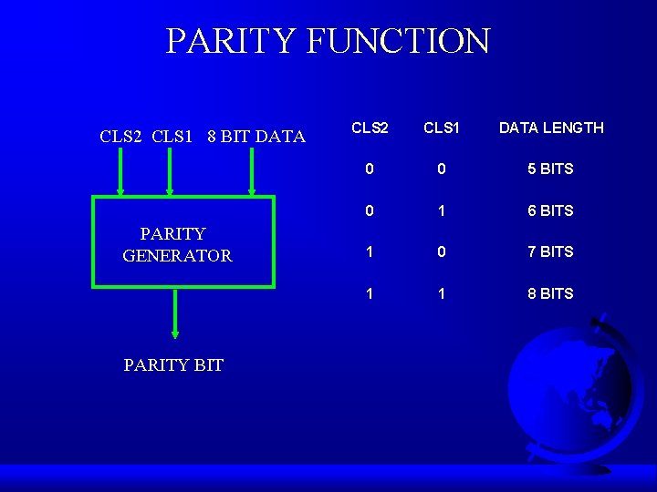
PARITY FUNCTION CLS 2 CLS 1 8 BIT DATA PARITY GENERATOR PARITY BIT CLS 2 CLS 1 DATA LENGTH 0 0 5 BITS 0 1 6 BITS 1 0 7 BITS 1 1 8 BITS

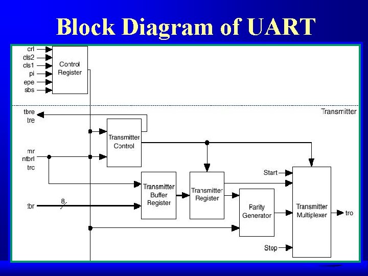
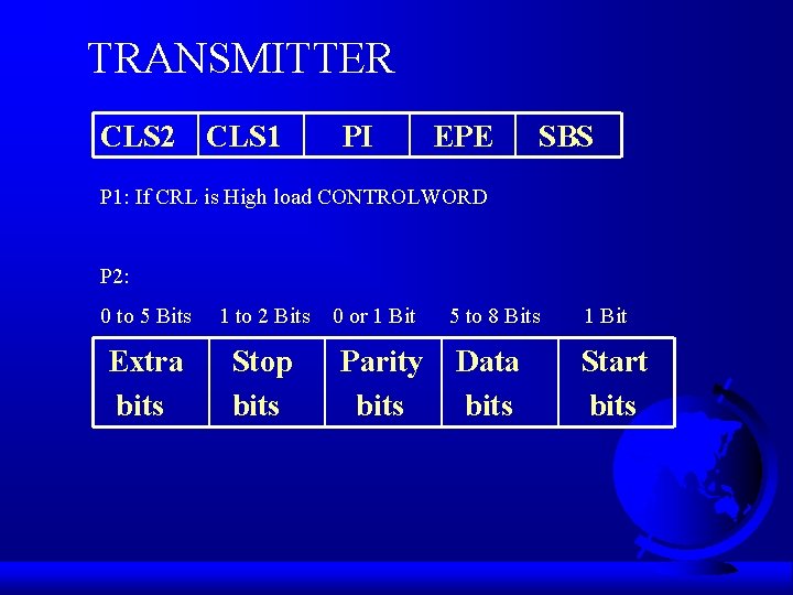
TRANSMITTER CLS 2 CLS 1 PI EPE SBS P 1: If CRL is High load CONTROLWORD P 2: 0 to 5 Bits 1 to 2 Bits Extra bits Stop bits 0 or 1 Bit Parity bits 5 to 8 Bits Data bits 1 Bit Start bits

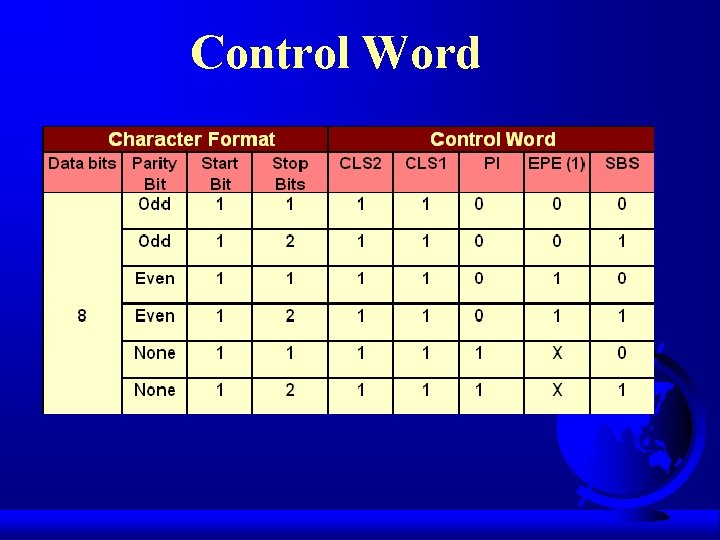
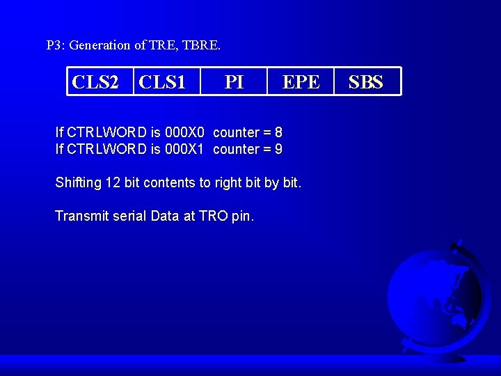
P 3: Generation of TRE, TBRE. CLS 2 CLS 1 PI EPE If CTRLWORD is 000 X 0 counter = 8 If CTRLWORD is 000 X 1 counter = 9 Shifting 12 bit contents to right bit by bit. Transmit serial Data at TRO pin. SBS

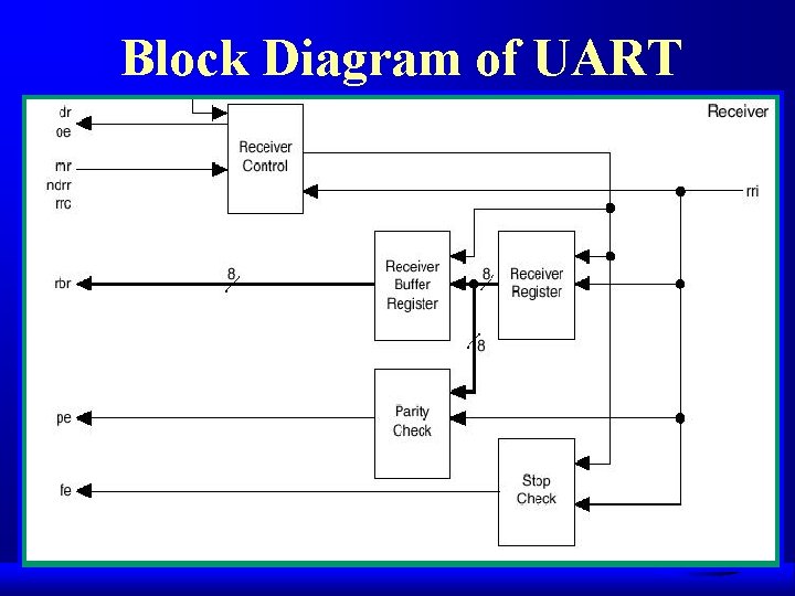
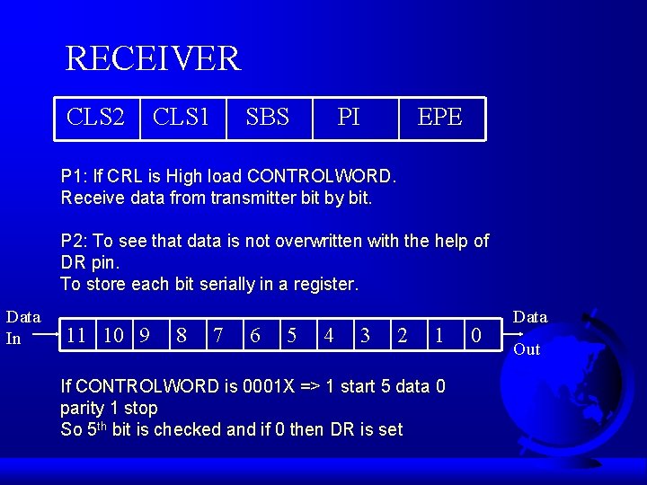
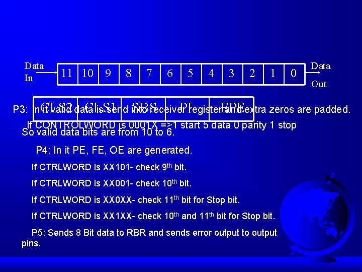
RECEIVER CLS 2 CLS 1 SBS PI EPE P 1: If CRL is High load CONTROLWORD. Receive data from transmitter bit by bit. P 2: To see that data is not overwritten with the help of DR pin. To store each bit serially in a register. Data In 11 10 9 8 7 6 5 4 3 2 1 If CONTROLWORD is 0001 X => 1 start 5 data 0 parity 1 stop So 5 th bit is checked and if 0 then DR is set 0 Data Out

Data In 11 10 9 8 7 6 5 4 3 2 1 0 Data Out CLS 1 SBSreceiver. PIregister. EPE P 3: In. CLS 2 it valid data is send into and extra zeros are padded. If CONTROLWORD is 0001 X =>1 start 5 data 0 parity 1 stop So valid data bits are from 10 to 6. P 4: In it PE, FE, OE are generated. If CTRLWORD is XX 101 - check 9 th bit. If CTRLWORD is XX 001 - check 10 th bit. If CTRLWORD is XX 0 XX- check 11 th bit for Stop bit. If CTRLWORD is XX 1 XX- check 10 th and 11 th bit for Stop bit. P 5: Sends 8 Bit data to RBR and sends error output to output pins.
