Chapter 13 Shift Registers William Kleitz Digital Electronics
- Slides: 44

Chapter 13 Shift Registers William Kleitz Digital Electronics with VHDL, Quartus® II Version Copyright © 2006 by Pearson Education, Inc. Upper Saddle River, New Jersey 07458 All rights reserved.

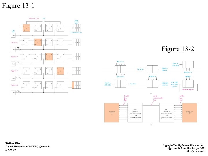
Shift Register Basics • Receives 4 bits of parallel data and shifts them to to right • Timing provided by the input clock • Shift right by one position each clock pulse • See Figure 13 -1 • Parallel format or Serial format • Shift Register operations - See Figure 13 -2 William Kleitz Digital Electronics with VHDL, Quartus® II Version Copyright © 2006 by Pearson Education, Inc. Upper Saddle River, New Jersey 07458 All rights reserved.

Figure 13 -1 Figure 13 -2 William Kleitz Digital Electronics with VHDL, Quartus® II Version Copyright © 2006 by Pearson Education, Inc. Upper Saddle River, New Jersey 07458 All rights reserved.

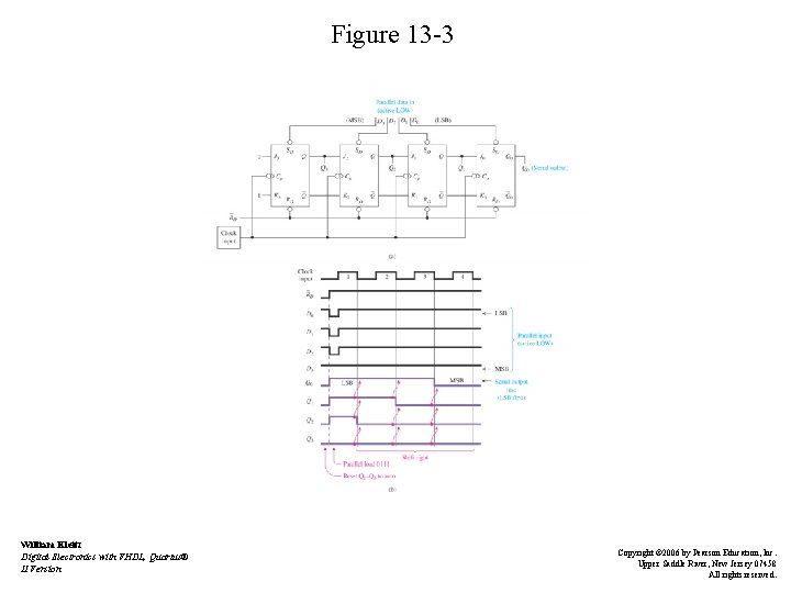
Parallel-to-Serial Conversion • 4 -bit parallel-in, serial-out shift register • See Figure 13 -3 William Kleitz Digital Electronics with VHDL, Quartus® II Version Copyright © 2006 by Pearson Education, Inc. Upper Saddle River, New Jersey 07458 All rights reserved.

Figure 13 -3 William Kleitz Digital Electronics with VHDL, Quartus® II Version Copyright © 2006 by Pearson Education, Inc. Upper Saddle River, New Jersey 07458 All rights reserved.

Recirculating Register • Rightmost data bit goes back to the input • See Figure 13 -3 William Kleitz Digital Electronics with VHDL, Quartus® II Version Copyright © 2006 by Pearson Education, Inc. Upper Saddle River, New Jersey 07458 All rights reserved.

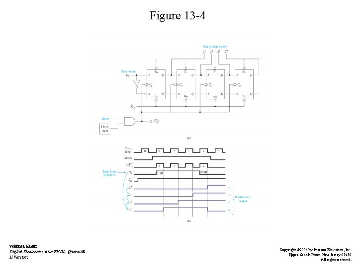
Serial-to-Parallel Conversion • • Serial-in, Parallel-out See Figure 13 -4 Inverter required at Ds Strobe line used to enable-then-disable the clock to stop the process William Kleitz Digital Electronics with VHDL, Quartus® II Version Copyright © 2006 by Pearson Education, Inc. Upper Saddle River, New Jersey 07458 All rights reserved.

Figure 13 -4 William Kleitz Digital Electronics with VHDL, Quartus® II Version Copyright © 2006 by Pearson Education, Inc. Upper Saddle River, New Jersey 07458 All rights reserved.

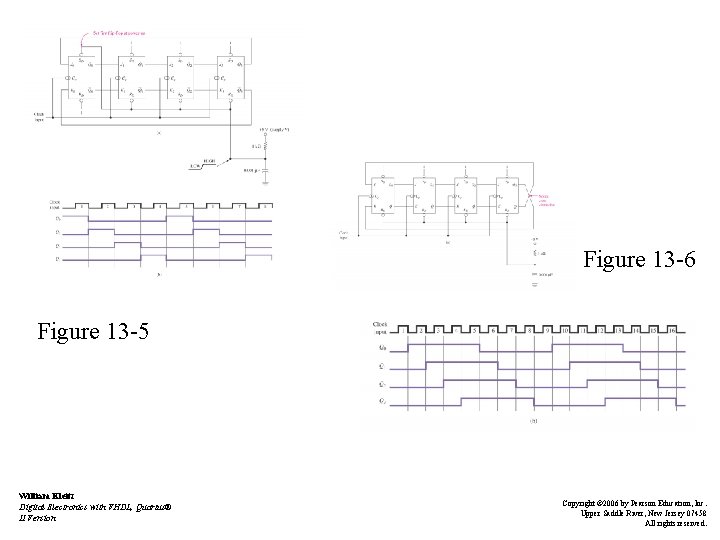
Ring Shift Counter and Johnson Shift Counter • Used to control digital sequences • 4 -bit ring shift counter – See Figure 13 -5 • Johnson Shift counter – See Figure 13 -6 William Kleitz Digital Electronics with VHDL, Quartus® II Version Copyright © 2006 by Pearson Education, Inc. Upper Saddle River, New Jersey 07458 All rights reserved.

Figure 13 -6 Figure 13 -5 William Kleitz Digital Electronics with VHDL, Quartus® II Version Copyright © 2006 by Pearson Education, Inc. Upper Saddle River, New Jersey 07458 All rights reserved.

VHDL Description of Shift Registers • Design flexibility – shift left or shift right – synchronous or asynchronous parallel loading – strobing the clock – recirculating data bits William Kleitz Digital Electronics with VHDL, Quartus® II Version Copyright © 2006 by Pearson Education, Inc. Upper Saddle River, New Jersey 07458 All rights reserved.

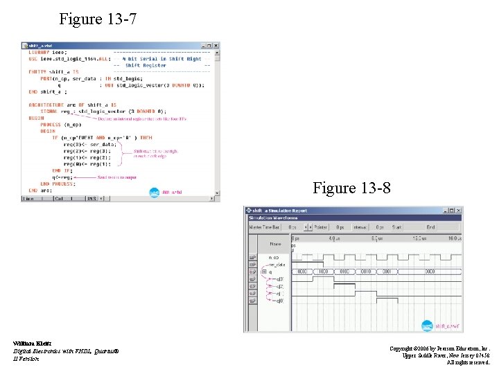
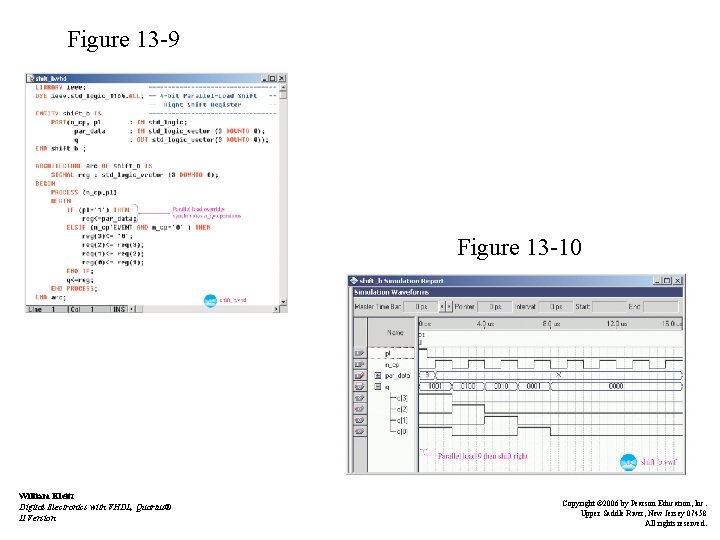
VHDL Description of Shift Registers • Serial-in shift right shift register – see figure 13 -7 and 13 -8 • Parallel load shift right shift register – see figure 13 -9 and 13 -10 William Kleitz Digital Electronics with VHDL, Quartus® II Version Copyright © 2006 by Pearson Education, Inc. Upper Saddle River, New Jersey 07458 All rights reserved.

Figure 13 -7 Figure 13 -8 William Kleitz Digital Electronics with VHDL, Quartus® II Version Copyright © 2006 by Pearson Education, Inc. Upper Saddle River, New Jersey 07458 All rights reserved.

Figure 13 -9 Figure 13 -10 William Kleitz Digital Electronics with VHDL, Quartus® II Version Copyright © 2006 by Pearson Education, Inc. Upper Saddle River, New Jersey 07458 All rights reserved.

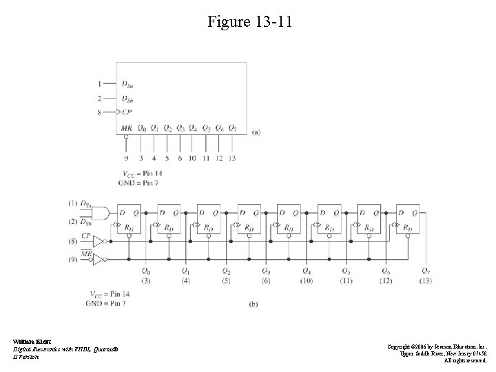
Shift Register ICs • • • 74164 8 -bit Serial-In, Parallel-Out 2 serial input lines Positive edge-triggered clock Active-LOW Master Reset See Figure 13 -11 – logic symbol – logic diagram William Kleitz Digital Electronics with VHDL, Quartus® II Version Copyright © 2006 by Pearson Education, Inc. Upper Saddle River, New Jersey 07458 All rights reserved.

Figure 13 -11 William Kleitz Digital Electronics with VHDL, Quartus® II Version Copyright © 2006 by Pearson Education, Inc. Upper Saddle River, New Jersey 07458 All rights reserved.

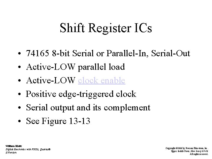
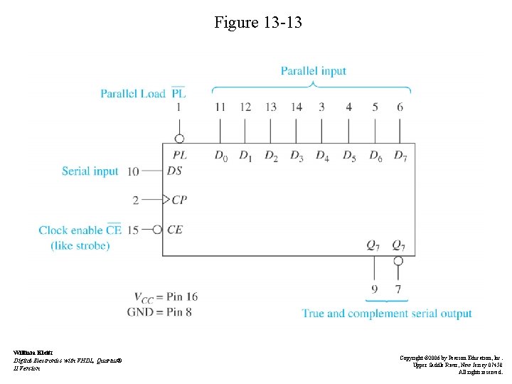
Shift Register ICs • • • 74165 8 -bit Serial or Parallel-In, Serial-Out Active-LOW parallel load Active-LOW clock enable Positive edge-triggered clock Serial output and its complement See Figure 13 -13 William Kleitz Digital Electronics with VHDL, Quartus® II Version Copyright © 2006 by Pearson Education, Inc. Upper Saddle River, New Jersey 07458 All rights reserved.

Figure 13 -13 William Kleitz Digital Electronics with VHDL, Quartus® II Version Copyright © 2006 by Pearson Education, Inc. Upper Saddle River, New Jersey 07458 All rights reserved.

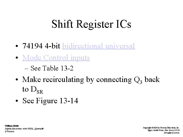
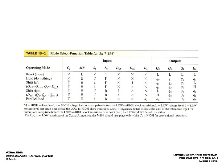
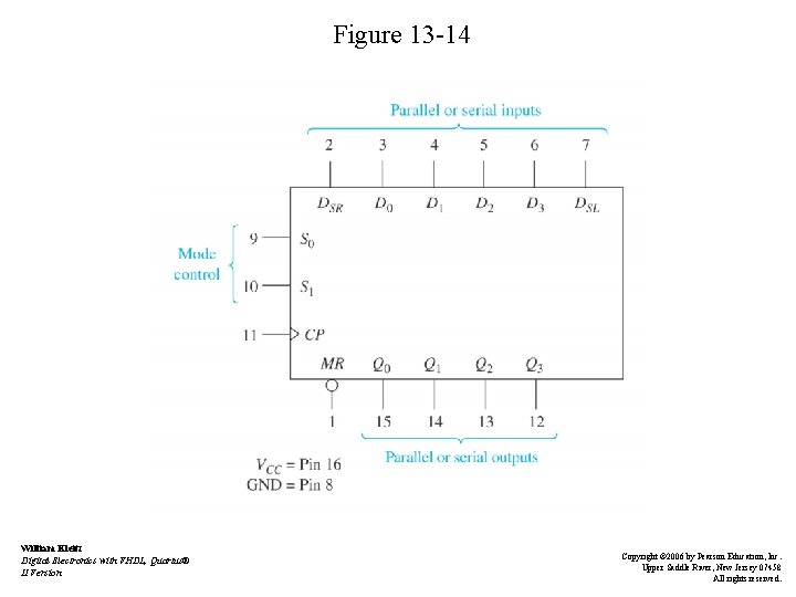
Shift Register ICs • 74194 4 -bit bidirectional universal • Mode Control inputs – See Table 13 -2 • Make recirculating by connecting Q 3 back to DSR • See Figure 13 -14 William Kleitz Digital Electronics with VHDL, Quartus® II Version Copyright © 2006 by Pearson Education, Inc. Upper Saddle River, New Jersey 07458 All rights reserved.

William Kleitz Digital Electronics with VHDL, Quartus® II Version Copyright © 2006 by Pearson Education, Inc. Upper Saddle River, New Jersey 07458 All rights reserved.

Figure 13 -14 William Kleitz Digital Electronics with VHDL, Quartus® II Version Copyright © 2006 by Pearson Education, Inc. Upper Saddle River, New Jersey 07458 All rights reserved.

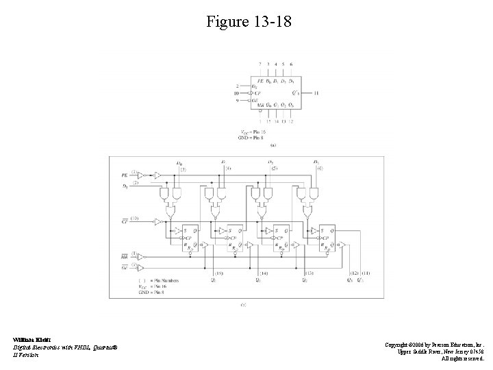
Shift Register ICs • Three-State Outputs – HIGH, LOW or float (high-impedance state) – used to connect output of more than one register to the same points – 74395 A 4 -bit shift register with tri-state outputs – See Figure 13 -18 • logic symbol • logic circuit William Kleitz Digital Electronics with VHDL, Quartus® II Version Copyright © 2006 by Pearson Education, Inc. Upper Saddle River, New Jersey 07458 All rights reserved.

Figure 13 -18 William Kleitz Digital Electronics with VHDL, Quartus® II Version Copyright © 2006 by Pearson Education, Inc. Upper Saddle River, New Jersey 07458 All rights reserved.

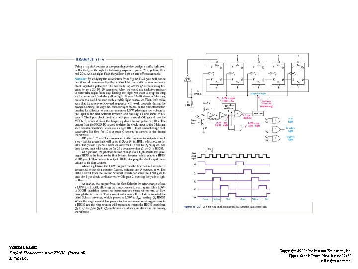
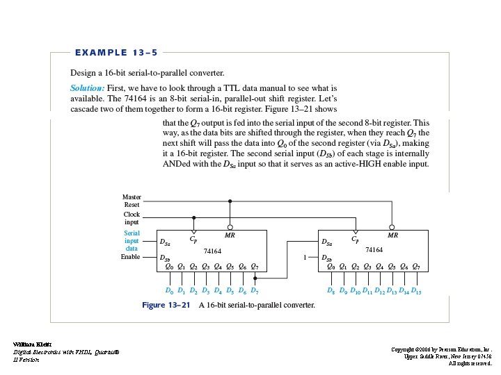
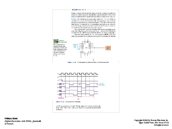
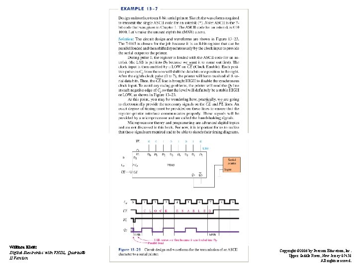
System Design Applications for Shift Registers • Traffic light controller – See Example 13 -4 • 16 -bit serial-to-parallel converter – See Example 13 -5 • Parallel-to-serial conversion – See Example 13 -6 • Interface to an 8 -bit serial printer – See Example 13 -7 William Kleitz Digital Electronics with VHDL, Quartus® II Version Copyright © 2006 by Pearson Education, Inc. Upper Saddle River, New Jersey 07458 All rights reserved.

William Kleitz Digital Electronics with VHDL, Quartus® II Version Copyright © 2006 by Pearson Education, Inc. Upper Saddle River, New Jersey 07458 All rights reserved.

William Kleitz Digital Electronics with VHDL, Quartus® II Version Copyright © 2006 by Pearson Education, Inc. Upper Saddle River, New Jersey 07458 All rights reserved.

William Kleitz Digital Electronics with VHDL, Quartus® II Version Copyright © 2006 by Pearson Education, Inc. Upper Saddle River, New Jersey 07458 All rights reserved.

William Kleitz Digital Electronics with VHDL, Quartus® II Version Copyright © 2006 by Pearson Education, Inc. Upper Saddle River, New Jersey 07458 All rights reserved.

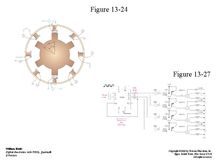
Driving a Stepper Motor with a Shift Register • Stepper motor makes rotation in steps • Driven by sequential digital signals • Made of stator with pole pairs and rotor with ferromagnetic pairs • See Figure 13 -24 • Drive Circuitry - See Figure 13 -27 William Kleitz Digital Electronics with VHDL, Quartus® II Version Copyright © 2006 by Pearson Education, Inc. Upper Saddle River, New Jersey 07458 All rights reserved.

Figure 13 -24 Figure 13 -27 William Kleitz Digital Electronics with VHDL, Quartus® II Version Copyright © 2006 by Pearson Education, Inc. Upper Saddle River, New Jersey 07458 All rights reserved.

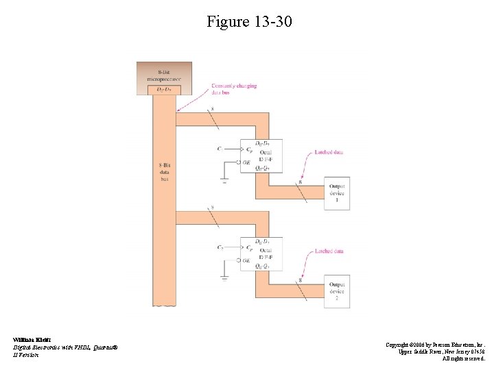
Three-State Buffers, Latches and Transceivers • Three State Buffers – when output devices must share same data bus – provides isolation – active-LOW Output Enable • Octal Latches/Flip-Flops – eight data lines simultaneously – See Figure 13 -30 William Kleitz Digital Electronics with VHDL, Quartus® II Version Copyright © 2006 by Pearson Education, Inc. Upper Saddle River, New Jersey 07458 All rights reserved.

Figure 13 -30 William Kleitz Digital Electronics with VHDL, Quartus® II Version Copyright © 2006 by Pearson Education, Inc. Upper Saddle River, New Jersey 07458 All rights reserved.

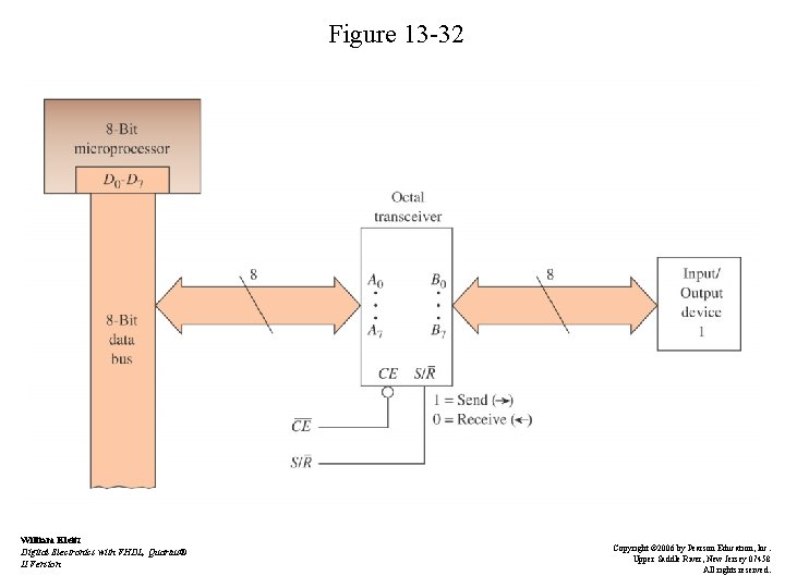
Three-State Buffers, Latches and Transceivers • Transceivers – transmitter/receiver – bidirectional – for both input to and output from a microprocessor – See Figure 13 -32 William Kleitz Digital Electronics with VHDL, Quartus® II Version Copyright © 2006 by Pearson Education, Inc. Upper Saddle River, New Jersey 07458 All rights reserved.

Figure 13 -32 William Kleitz Digital Electronics with VHDL, Quartus® II Version Copyright © 2006 by Pearson Education, Inc. Upper Saddle River, New Jersey 07458 All rights reserved.

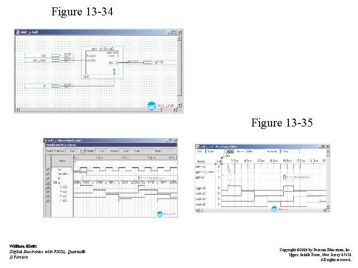
Using the LPM Shift Register and 74194 Macrofunction • General purpose shift register in the library of parameterized modules: LPM_SHIFTREG – port/parameters options • • LPM_WIDTH serial or parallel I/O asynch or synch loading clock enable – example of serial in, shift right, with synch parallel loading – see figure 13 -34 and 13 -35 William Kleitz Digital Electronics with VHDL, Quartus® II Version Copyright © 2006 by Pearson Education, Inc. Upper Saddle River, New Jersey 07458 All rights reserved.

Figure 13 -34 Figure 13 -35 William Kleitz Digital Electronics with VHDL, Quartus® II Version Copyright © 2006 by Pearson Education, Inc. Upper Saddle River, New Jersey 07458 All rights reserved.

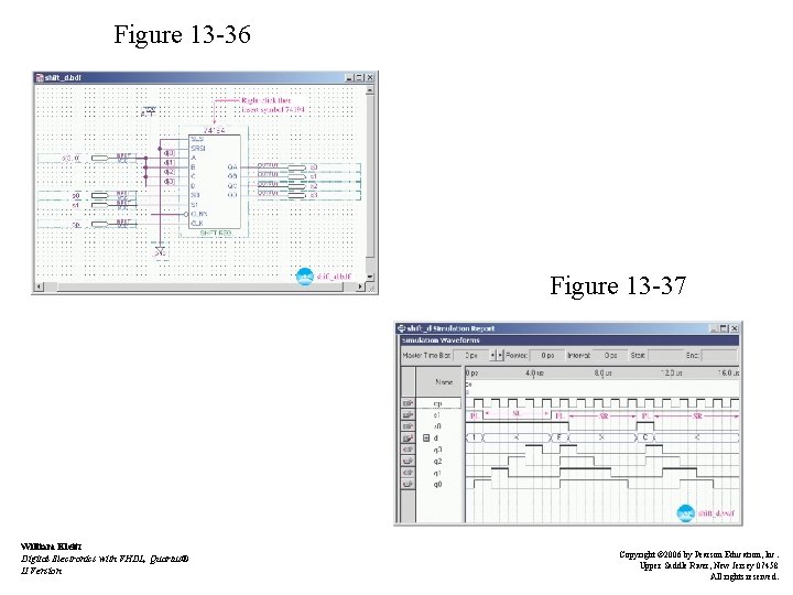
Using the LPM Shift Register and 74194 Macrofunction • 7400 series are provided as macrofunctions • The 74194 as a universal shift register – see figure 13 -36 and 13 -37 William Kleitz Digital Electronics with VHDL, Quartus® II Version Copyright © 2006 by Pearson Education, Inc. Upper Saddle River, New Jersey 07458 All rights reserved.

Figure 13 -36 Figure 13 -37 William Kleitz Digital Electronics with VHDL, Quartus® II Version Copyright © 2006 by Pearson Education, Inc. Upper Saddle River, New Jersey 07458 All rights reserved.

Summary • Shift registers are used for serial-to-parallel and parallel-to-serial conversions. • One common form of digital communication is for a sending computer to convert its data from parallel to serial and then transmit over a telephone line to a receiving computer, which converts back from serial to parallel. William Kleitz Digital Electronics with VHDL, Quartus® II Version Copyright © 2006 by Pearson Education, Inc. Upper Saddle River, New Jersey 07458 All rights reserved.

Summary • Simple shift registers can be constructed by connecting the Q-outputs on one J-K flipflop into the J-K inputs of the next flip-flop. Several flip-flops can be cascaded together this way, driven by a common clock, to form multibit shift registers. • The ring and Johnson shift counters are two specialized shift registers used to create sequential control waveforms. William Kleitz Digital Electronics with VHDL, Quartus® II Version Copyright © 2006 by Pearson Education, Inc. Upper Saddle River, New Jersey 07458 All rights reserved.

Summary • Several multibit shift register ICs are available for the designer to choose from. They generally have four or eight internal flip-flops and are designed to shift either left or right and perform either serial-to-parallel or parallel-to-serial conversions. • The 74194 is called a universal 4 -bit shift register, because it can shift in either direction and can receive and convert to either format. William Kleitz Digital Electronics with VHDL, Quartus® II Version Copyright © 2006 by Pearson Education, Inc. Upper Saddle River, New Jersey 07458 All rights reserved.

Summary • Three-state outputs are used on ICs that must have their outputs go to a common point. They are capable of the normal HIGH/LOW levels but can also output a float (or high-impedance) state. • The rotation of a stepper motor is made by taking small angular steps. This is controlled by sequential digital strings often generated by a recirculating shift register. William Kleitz Digital Electronics with VHDL, Quartus® II Version Copyright © 2006 by Pearson Education, Inc. Upper Saddle River, New Jersey 07458 All rights reserved.

Summary • Three-state buffers, latches and transceivers are an integral part of microprocessor interface circuitry. They allow the microprocessor system to have external control of 8 -bit groups of data. The buffer can be used to allow multiple inputs devices to feed a common point or to provide high output current to a connected load. William Kleitz Digital Electronics with VHDL, Quartus® II Version Copyright © 2006 by Pearson Education, Inc. Upper Saddle River, New Jersey 07458 All rights reserved.

Summary • The latch can be used to remember momentary data from the microprocessor that needs to be held for other devices in the system. The transceiver provides bidirectional (input or output) control of interface circuitry. William Kleitz Digital Electronics with VHDL, Quartus® II Version Copyright © 2006 by Pearson Education, Inc. Upper Saddle River, New Jersey 07458 All rights reserved.