EET 2023 DIGITAL ELECTRONICS II CHAPTER 2 REGISTERS


 (Left Shift)")
")
")
")
")
")
")
")


, BCD counts")


- Slides: 28
EET 202/3 DIGITAL ELECTRONICS II CHAPTER 2 : REGISTERS & REGISTERS TRANSFER Semester 1 Session 2015/2016
Microoperations on a Single 2. 3 Register ~ Outline ~ Shift Registers q. Counters q OBJECTIVE S OF THIS CHAPTER CO 1: Ability to construct dig ital logic circuit using Register Transfer Lan guage
Shift Registers move data laterally within the register toward its MSB or LSB position In the simplest case, the shift register is simply a set of D flip-flops connected in a row like this: *CP: a common clock pulse input that activates the shift
Shift Registers Parallel Output Serial Input Serial Output Data input, In, is called a serial input or the shift right input. Data output, Out, is often called the serial output. The vector (A, B, C, Out) is called the parallel output.
Shift Registers with Parallel Load The shift register shown earlier has no control input, thus data is always shifted on clock pulse. How to make the shift registers more controllable? E. g. shifts only on select positive clock edges. Shift operation can be controlled through D inputs of the FFs, rather than through the clock inputs CP.
Shift Registers with Parallel Load By adding a mux between each shift register stage, data can be shifted or loaded Serial Input 2 -to-1 MUX Dn A 0 IN A 1 Selector SHIFT If SHIFT is LOW, A and B are replaced by the data on DA and DB lines, else data shifts right on each clock.
Bidirectional Shift Register Unidirectional Register Capable of shifting in only one direction (like what we have discussed in previous lectures) 1. Shift on clock pulse 2. Shift & Load 3. Shift, Load & Hold * shift occurs in one direction only Bidirectional Register A register that can shift in both directions 1. Shift Left (sl) 2. Shift Right (sr) And at the same time is capable of HOLD and LOAD
Bidirectional Shift Register A 0 A 1 A 2 A 3 By placing a 4 -input multiplexer in front of each D flip-flop in a shift register, we can implement a circuit with shift right, shift left, parallel load, hold. 0 1 2 3 4 -to -1 MUX S 0 S 1 D S 1 S 0 Register Operation 0 0 1 1 0 1 No change (hold) Shift Left Shift Right Parallel Load Each stage consists of a D-FF and 4: 1 multiplexer
DOWN HOLD Parallel load UP Bidirectional Shift Register Let’s analyze the one stage diagram of a Bidirectional Shift Register with parallel load. S 1 S 0 Register Operation 0 0 No change (Hold) 0 1 Shift Left (down) 1 0 Shift Right (up) 1 1 Parallel Load
Bidirectional Shift Register How do we represent this in RTL? ? S 1 S 0 Register Operation 0 0 1 1 0 1 No change (hold) Shift Left (down) Shift Right (up) Parallel Load
4 -Bit Bidirectional Shift Register with Parallel Load Serial outputs: (Right Shift) (Left Shift) sr LSI sl MSB LSB 7 6 5 4 3 2 1 0 RSI
Exercise (Tutorial 2)
Exercise (Tutorial 2)
Exercise (MTE 2013)
Exercise (MTE 2014)
Exercise (FE 2012)
Exercise (FE 2012)
Exercise (FE 2014)
Counter A register that goes through a prescribed sequence of distinct states upon the application of a sequence of input pulses. Input pulses may be clock pulses or from other source, may occur at regular or irregular intervals of time. Binary counter: a counter that follows the binary number sequence. n n FFs An n-bit binary counter consists of Can count in binary from 0 through 2 -1 Counter are available in two categories; i. e. ripple counters and synchronous counters
BCD counter with parallel load Connect an external AND gate to Load Counter starts with allzero output (0000) Count input always HIGH (1) Load Count Action 0 0 Hold Stored Value 0 1 Count Up Stored Value 1 X Load D
BCD counter with parallel load AND gate = 0 (LOAD = 0), BCD counts from 0000 to 1001 Output = 1001, Q 0 and Q 3 in HIGH, AND gate = 1 (LOAD = 1) Next clock transition, counter load inputs (D 0 D 3) = 0000 following 1001 into counter. Load Count Action 0 0 Hold Stored Value 0 1 Count Up Stored Value 1 X Load D 1 1 0 1 0 0 0 1
BCD counter with parallel load Y
BCD code
BCD counter with parallel load
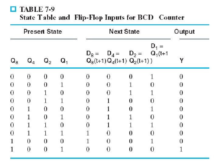
Exercise Figure 2. 5 shows the symbol of 4 - bit BCD counter. Design the BCD counter below to follow counting from 0000 to 1001 complete with state table and k-map. Assume parallel load data is 0.