EET 2023 DIGITAL ELECTRONICS II CHAPTER 4 COMPUTER


- Slides: 61

EET 202/3 DIGITAL ELECTRONICS II CHAPTER 4 : COMPUTER DESIGN BASICS

Outline Datapath q Arithmetic/Logic Unit (ALU) q The Shifter q Datapath Representation OBJECTIVES q The Control Word OF THIS q CHAPTER CO 3: Ability to design and evaluate a basic computer sys tem

Datapath

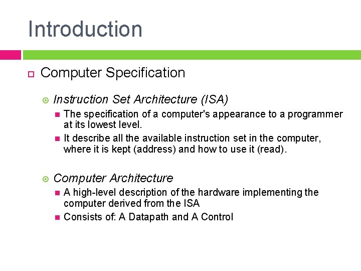
Introduction Computer Specification Instruction Set Architecture (ISA) The specification of a computer's appearance to a programmer at its lowest level. It describe all the available instruction set in the computer, where it is kept (address) and how to use it (read). Computer Architecture A high-level description of the hardware implementing the computer derived from the ISA Consists of: A Datapath and A Control

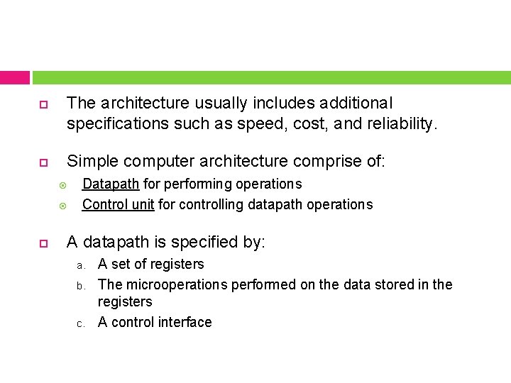
The architecture usually includes additional specifications such as speed, cost, and reliability. Simple computer architecture comprise of: Datapath for performing operations Control unit for controlling datapath operations A datapath is specified by: a. b. c. A set of registers The microoperations performed on the data stored in the registers A control interface

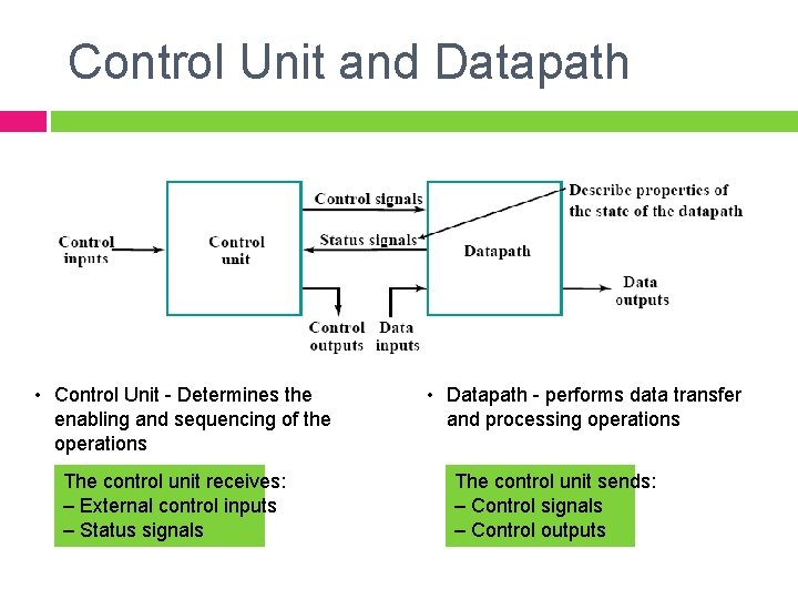
Control Unit and Datapath • Control Unit - Determines the enabling and sequencing of the operations The control unit receives: – External control inputs – Status signals • Datapath - performs data transfer and processing operations The control unit sends: – Control signals – Control outputs

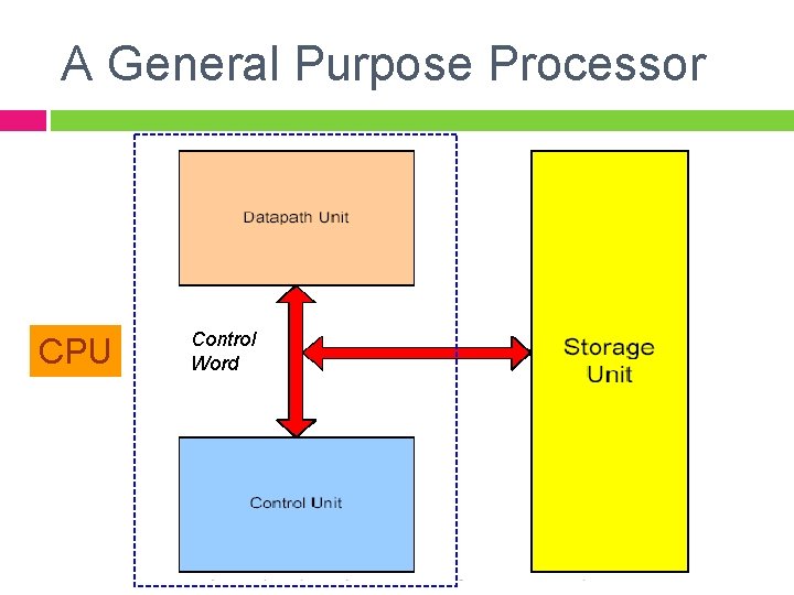
A General Purpose Processor CPU Control Word

Computer Datapath Implements register transfer microoperations and serves as a framework for the design of detailed processing logic. Control Word Provides a tie between the datapath and the control unit.

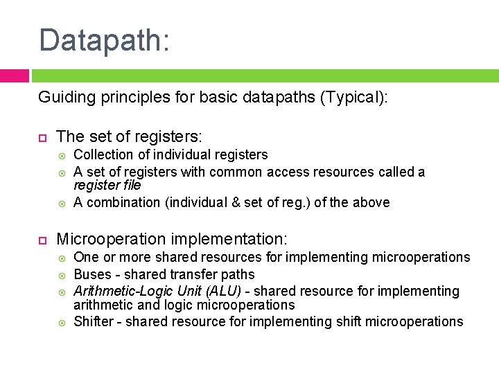
Datapath: Guiding principles for basic datapaths (Typical): The set of registers: Collection of individual registers A set of registers with common access resources called a register file A combination (individual & set of reg. ) of the above Microoperation implementation: One or more shared resources for implementing microoperations Buses - shared transfer paths Arithmetic-Logic Unit (ALU) - shared resource for implementing arithmetic and logic microoperations Shifter - shared resource for implementing shift microoperations

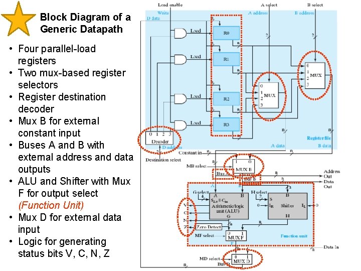
Block Diagram of a Generic Datapath • Four parallel-load registers • Two mux-based register selectors • Register destination decoder • Mux B for external constant input • Buses A and B with external address and data outputs • ALU and Shifter with Mux F for output select (Function Unit) • Mux D for external data input • Logic for generating status bits V, C, N, Z

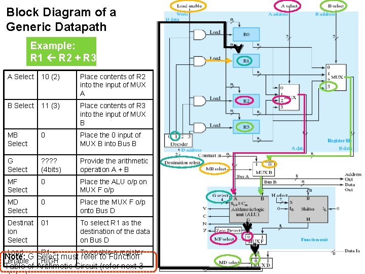
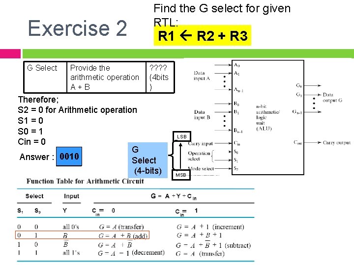
Block Diagram of a Generic Datapath Example: R 1 R 2 + R 3 A Select 10 (2) Place contents of R 2 into the input of MUX A B Select 11 (3) Place contents of R 3 into the input of MUX B MB Select 0 Place the 0 input of MUX B into Bus B G Select ? ? (4 bits) Provide the arithmetic operation A + B MF Select 0 Place the ALU o/p on MUX F o/p MD Select 0 Place the MUX F o/p onto Bus D Destinat ion Select 01 To select R 1 as the destination of the data on Bus D Load R 1 = To enable a register Note: G Select must refer to Function enable HIGH Table of Arithmetic Circuit (refer next 3

Arithmetic/Logic Unit (ALU)

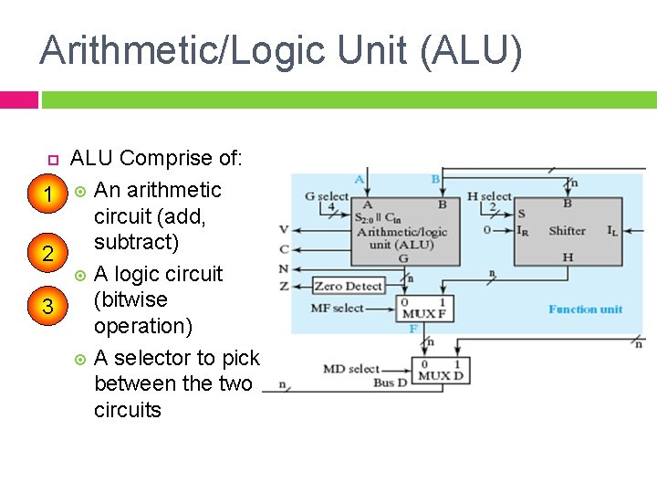
Arithmetic/Logic Unit (ALU) ALU Comprise of: 1 An arithmetic circuit (add, subtract) 2 A logic circuit (bitwise 3 operation) A selector to pick between the two circuits

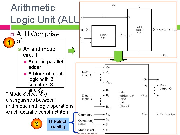
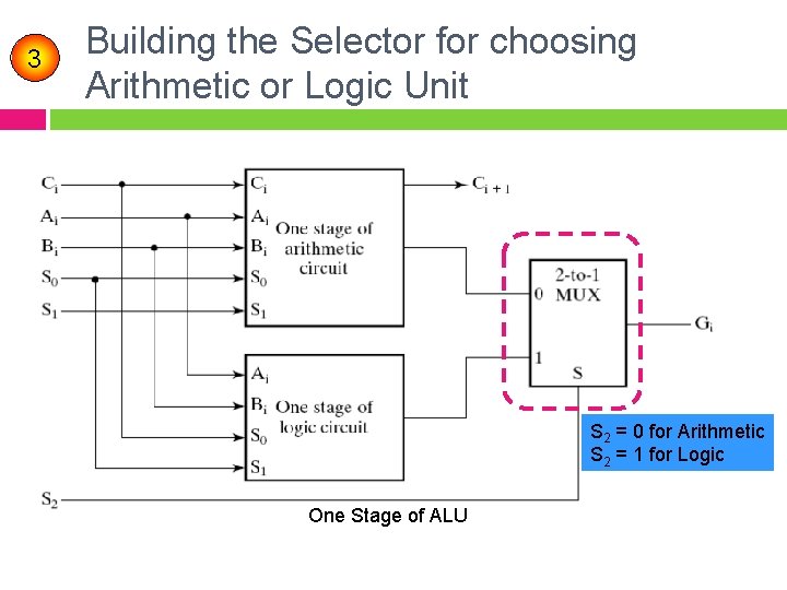
Arithmetic Logic Unit (ALU) ALU Comprise 1 of: An arithmetic circuit An n-bit parallel adder A block of input logic with 2 selectors S 1 and S 0 * Mode Select (S 2) distinguishes between arithmetic and logic operations which actually construct item 3 G Select (4 -bits)

ALU Is a combinational circuit that performs a set of basic microoperations on: Arithmetic, and Logic Has a number of selection lines used to determine the operations to be performed e. g. n selection lines can specify up to 2 n types of operations.

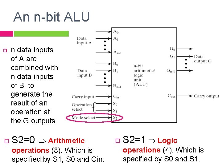
An n-bit ALU n data inputs of A are combined with n data inputs of B, to generate the result of an operation at the G outputs. S 2=0 Arithmetic operations (8). Which is specified by S 1, S 0 and Cin. S 2=1 Logic operations (4). Which is specified by S 0 and S 1.

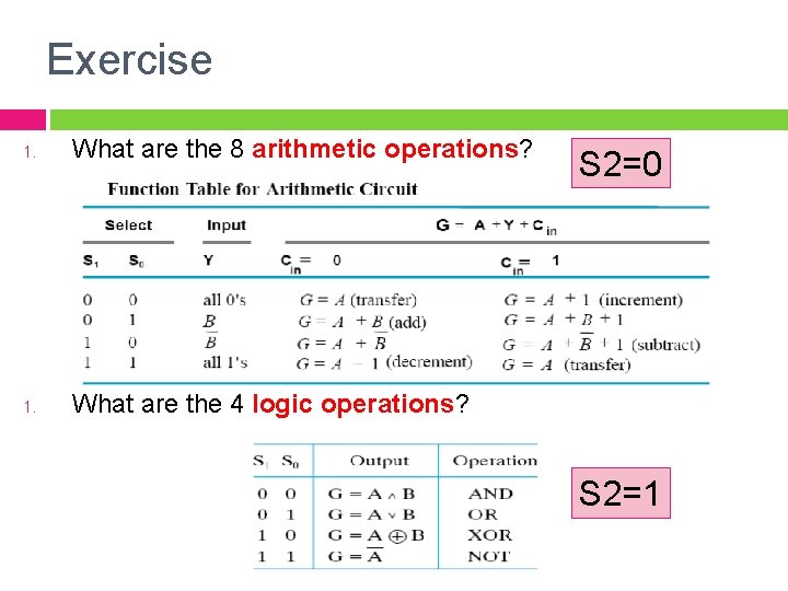
Exercise 1. What are the 8 arithmetic operations? 1. What are the 4 logic operations? S 2=0 S 2=1

How to design the ALU? 1. Design the arithmetic section 2. Design the logic section 3. Combine both sections

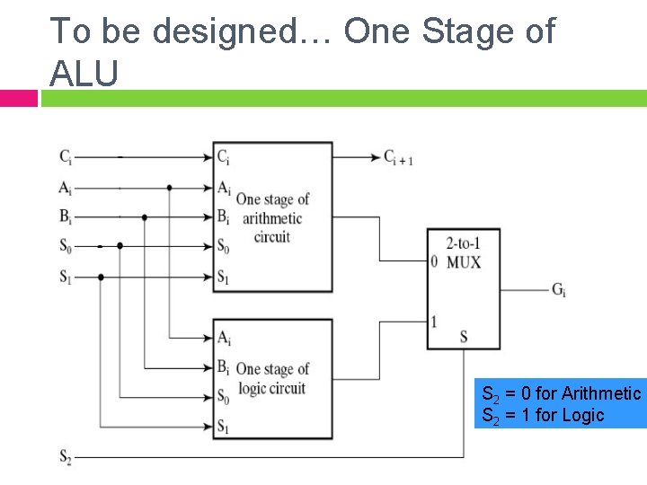
To be designed… One Stage of ALU S 2 = 0 for Arithmetic S 2 = 1 for Logic

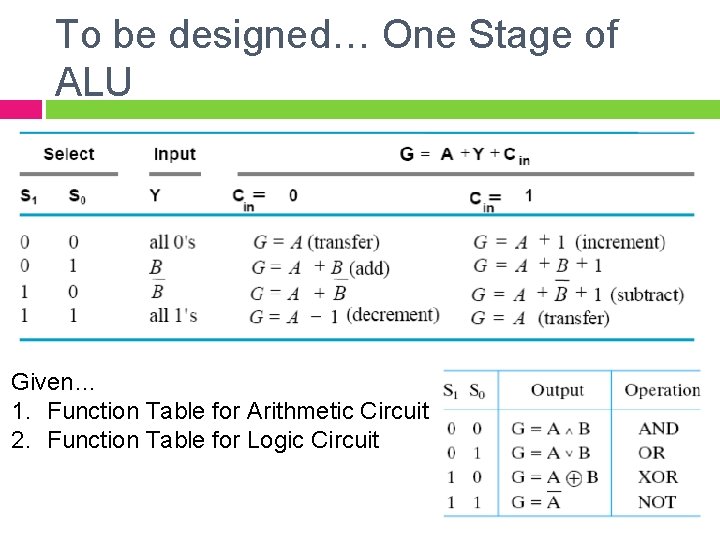
To be designed… One Stage of ALU Given… 1. Function Table for Arithmetic Circuit 2. Function Table for Logic Circuit

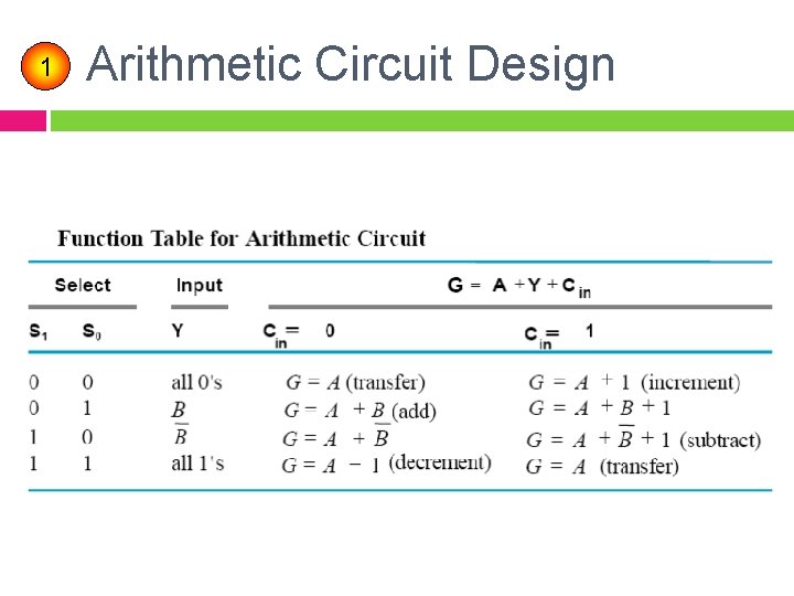
1 Arithmetic Circuit Design

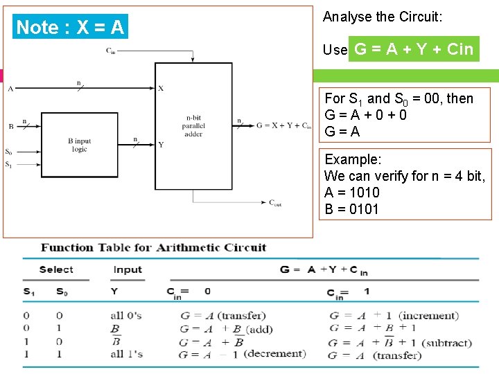
Note : X = A Analyse the Circuit: Use G = A + Y + Cin For S 1 and S 0 = 00, then G=A+0+0 G=A Example: We can verify for n = 4 bit, A = 1010 B = 0101

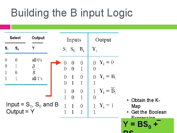
Building the B input Logic Output Input = S 1, S 0 and B Output = Y • Obtain the KMap • Get the Boolean Expression Y = BS 0 +

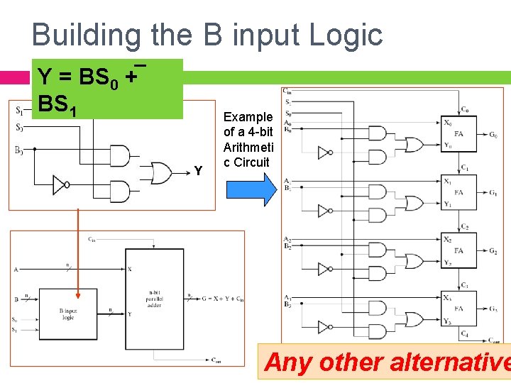
Building the B input Logic Y = BS 0 + BS 1 Y Example of a 4 -bit Arithmeti c Circuit Any other alternative

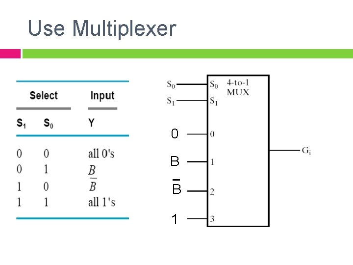
Use Multiplexer 0 B B 1

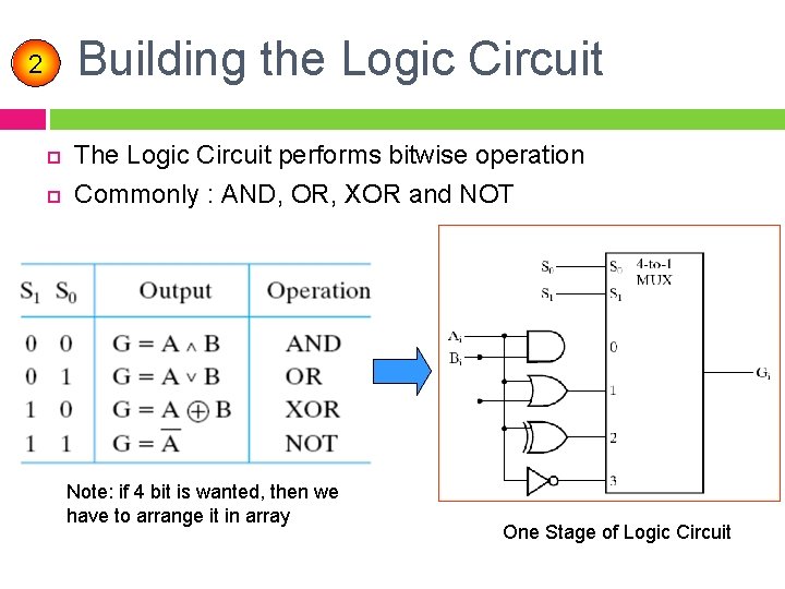
Building the Logic Circuit 2 The Logic Circuit performs bitwise operation Commonly : AND, OR, XOR and NOT Note: if 4 bit is wanted, then we have to arrange it in array One Stage of Logic Circuit

3 Building the Selector for choosing Arithmetic or Logic Unit S 2 = 0 for Arithmetic S 2 = 1 for Logic One Stage of ALU

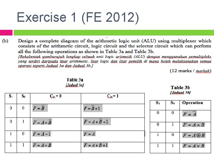
Exercise 1 (FE 2012)

Exercise 2 G Select Provide the arithmetic operation A+B Find the G select for given RTL: R 1 R 2 + R 3 ? ? (4 bits ) Therefore; S 2 = 0 for Arithmetic operation S 1 = 0 S 0 = 1 Cin = 0 G Answer : 0010 Select (4 -bits) LSB MSB

The Shifter

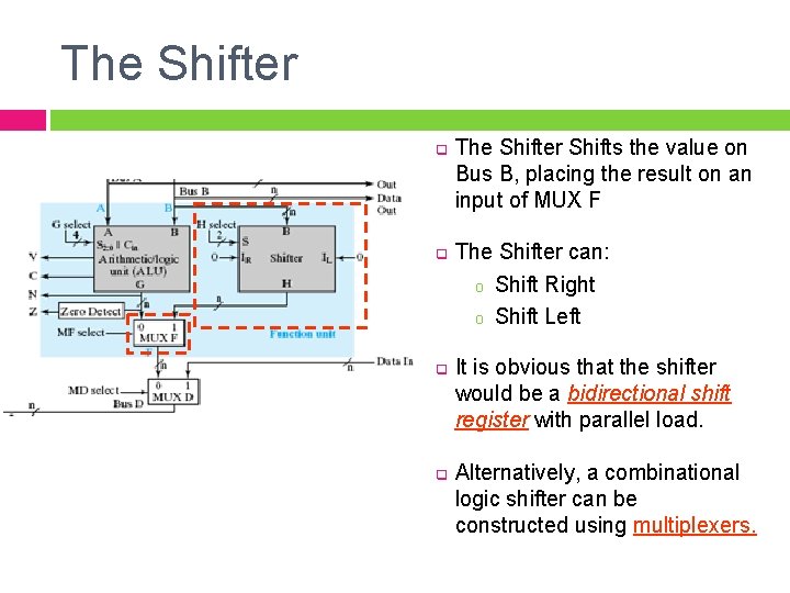
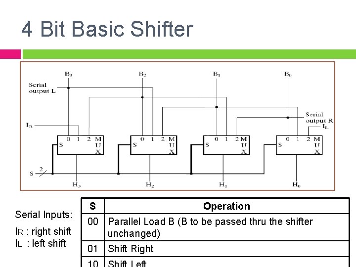
The Shifter q q The Shifter Shifts the value on Bus B, placing the result on an input of MUX F The Shifter can: o Shift Right o Shift Left It is obvious that the shifter would be a bidirectional shift register with parallel load. Alternatively, a combinational logic shifter can be constructed using multiplexers.

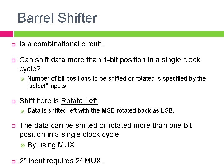
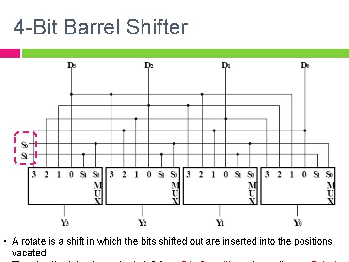
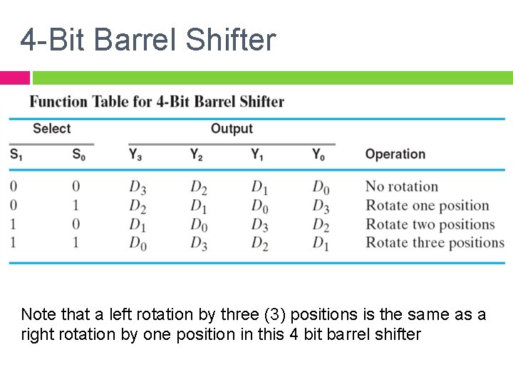
Barrel Shifter Is a combinational circuit. Can shift data more than 1 -bit position in a single clock cycle? Shift here is Rotate Left. Number of bit positions to be shifted or rotated is specified by the “select” inputs. Data is shifted left with the MSB rotated back as LSB. The data can be shifted or rotated more than one bit position in a single clock cycle By using MUX. 2 n input requires 2 n MUX.

Barrel Shifter The data can be shifted or rotated more than one bit position in a single clock cycle By using MUX. 2 n input requires 2 n MUX.

4 Bit Basic Shifter Serial Inputs: IR : right shift IL : left shift S Operation 00 Parallel Load B (B to be passed thru the shifter unchanged) 01 Shift Right

4 -Bit Barrel Shifter • A rotate is a shift in which the bits shifted out are inserted into the positions vacated

4 -Bit Barrel Shifter Note that a left rotation by three (3) positions is the same as a right rotation by one position in this 4 bit barrel shifter

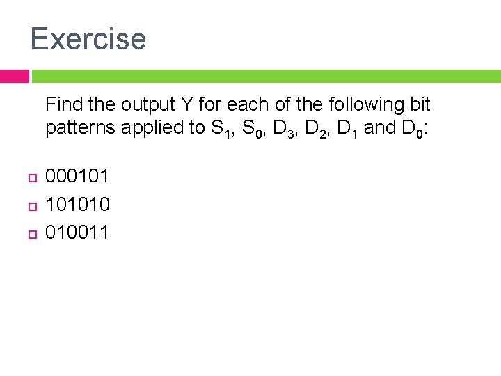
Exercise Find the output Y for each of the following bit patterns applied to S 1, S 0, D 3, D 2, D 1 and D 0: 000101 101010 010011

Datapath Representation

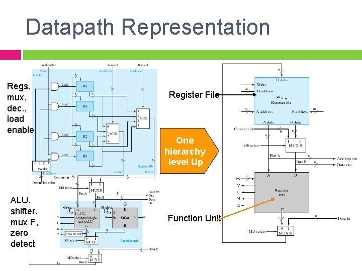
Datapath Representation Regs, mux, dec. , load enable Register File One hierarchy level Up ALU, shifter, mux F, zero detect Function Unit

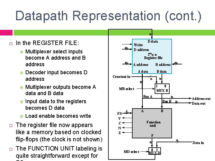
Datapath Representation (cont. ) n In the REGISTER FILE: m Multiplexer select inputs become A address and B address Decoder input becomes D address Multiplexer outputs become A data and B data m The register file now appears like a memory based on clocked flip-flops (the clock is not shown) The FUNCTION UNIT labeling is quite straightforward except for A address B address A data Constant in n 1 0 MUX B MB select Bus A FS V C N Z 4 m B data n n Input data to the registers becomes D data Load enable becomes write D data Write D address 2 mx n Register file A n Bus B n Address out Data out B Function unit F n MD select 0 1 MUX D n Data in

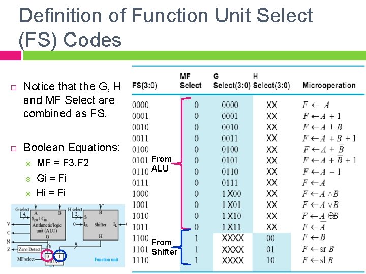
Definition of Function Unit Select (FS) Codes Notice that the G, H and MF Select are combined as FS. Boolean Equations: MF = F 3. F 2 Gi = Fi Hi = Fi From ALU From Shifter

Control Word

Control Word The datapath has many control inputs. The signals driving these inputs can be defined and organized into a control word. To execute a microinstruction, we apply control word values for a clock cycle. For most microoperations, the positive edge of the clock cycle is needed to perform the register load. The datapath control word format and the field definitions are shown on the next slide.

Control Word Represents the control inputs to the datapath. Determines the microoperation to be executed for each clock pulse.

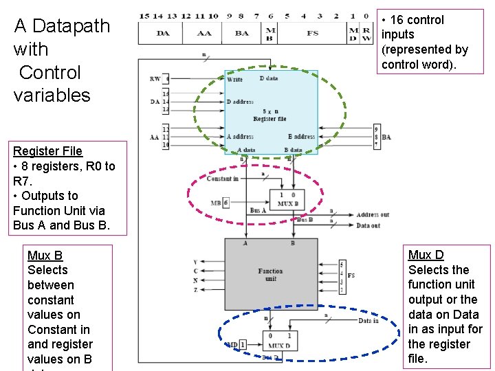
A Datapath with Control variables • 16 control inputs (represented by control word). Register File • 8 registers, R 0 to R 7. • Outputs to Function Unit via Bus A and Bus B. Mux B Selects between constant values on Constant in and register values on B Mux D Selects the function unit output or the data on Data in as input for the register file.

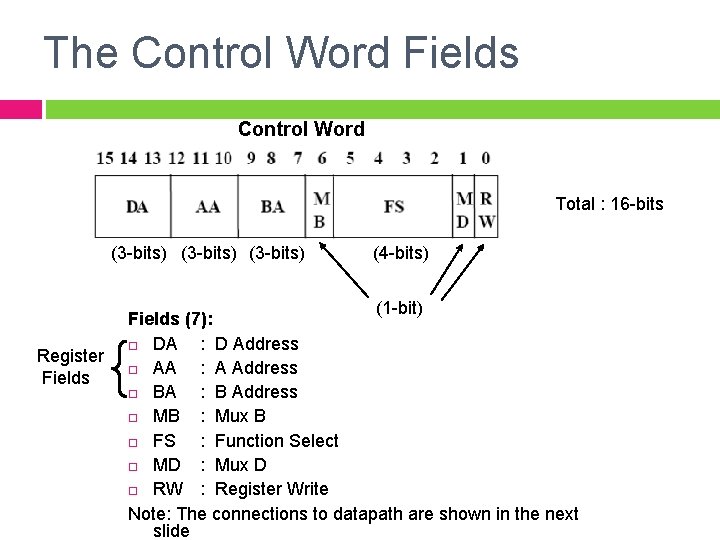
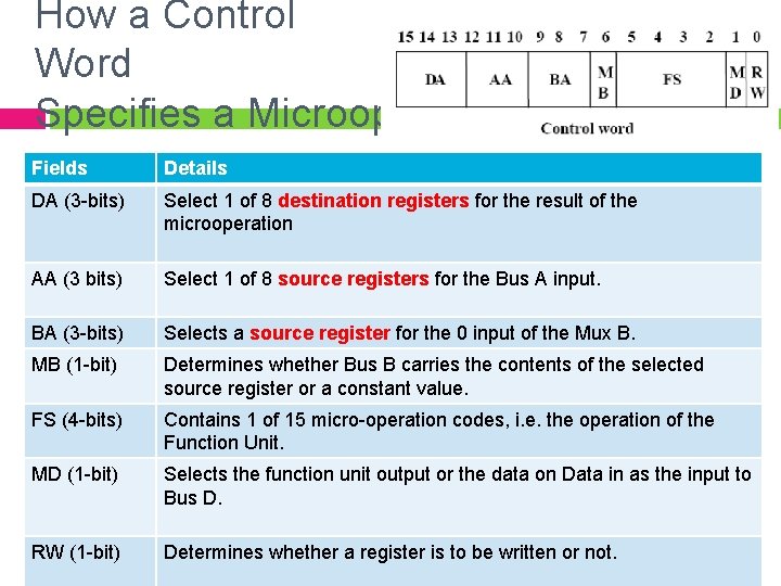
The Control Word Fields Control Word Total : 16 -bits (3 -bits) Register Fields (4 -bits) (1 -bit) Fields (7): DA : D Address AA : A Address BA : B Address MB : Mux B FS : Function Select MD : Mux D RW : Register Write Note: The connections to datapath are shown in the next slide

How a Control Word Specifies a Microop Fields Details DA (3 -bits) Select 1 of 8 destination registers for the result of the microoperation AA (3 bits) Select 1 of 8 source registers for the Bus A input. BA (3 -bits) Selects a source register for the 0 input of the Mux B. MB (1 -bit) Determines whether Bus B carries the contents of the selected source register or a constant value. FS (4 -bits) Contains 1 of 15 micro-operation codes, i. e. the operation of the Function Unit. MD (1 -bit) Selects the function unit output or the data on Data in as the input to Bus D. RW (1 -bit) Determines whether a register is to be written or not.

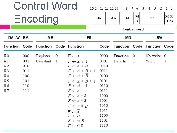
Control Word Encoding

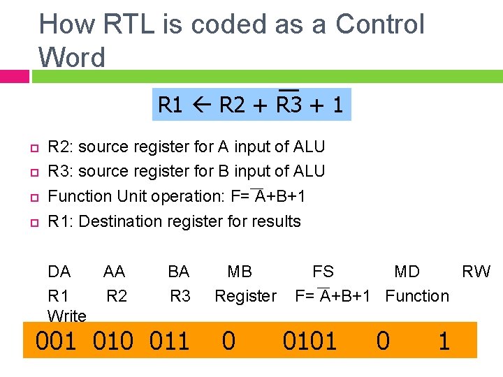
How RTL is coded as a Control Word R 1 R 2 + R 3 + 1 R 2: source register for A input of ALU R 3: source register for B input of ALU Function Unit operation: F= A+B+1 R 1: Destination register for results DA AA R 1 R 2 Write BA R 3 001 010 011 MB Register 0 FS MD RW F= A+B+1 Function 0101 0 1

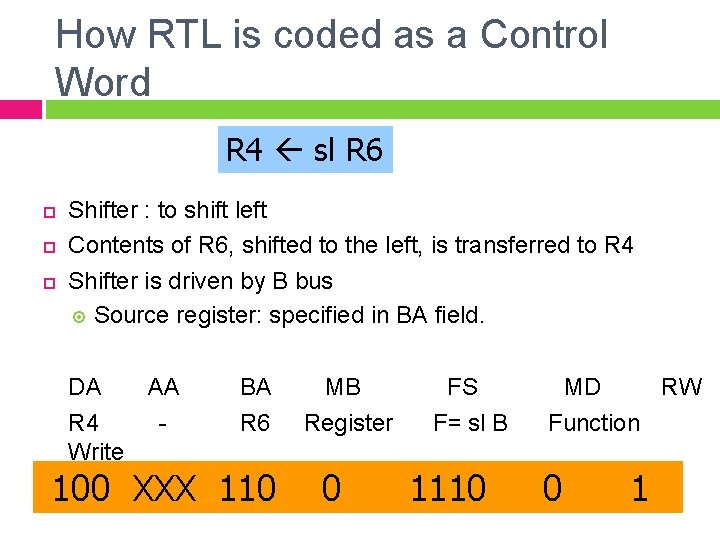
How RTL is coded as a Control Word R 4 sl R 6 Shifter : to shift left Contents of R 6, shifted to the left, is transferred to R 4 Shifter is driven by B bus Source register: specified in BA field. DA AA R 4 Write BA R 6 100 XXX 110 MB Register 0 FS F= sl B 1110 MD RW Function 0 1

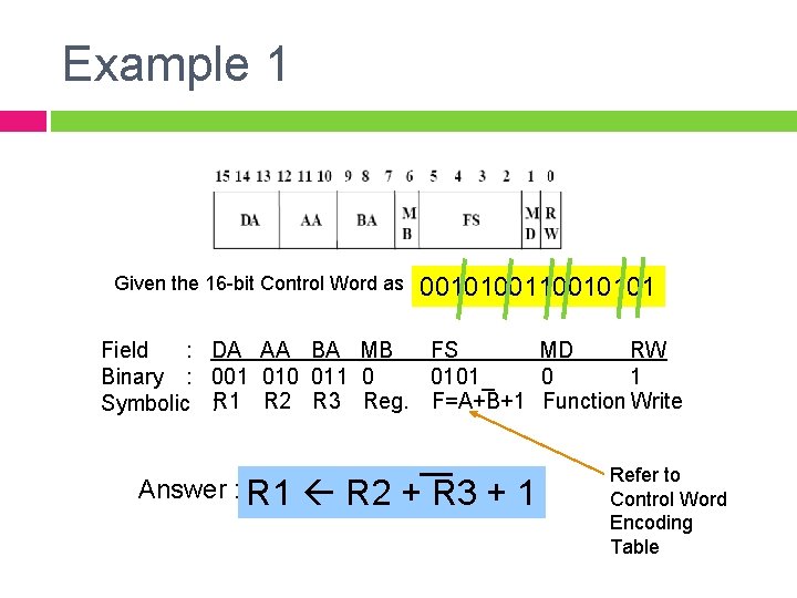
Example 1 Given the 16 -bit Control Word as 001010010101 Field : DA AA BA MB FS MD RW Binary : 001 010 011 0 0101 0 1 Symbolic : R 1 R 2 R 3 Reg. F=A+B+1 Function Write Answer : R 1 R 2 + R 3 + 1 Refer to Control Word Encoding Table

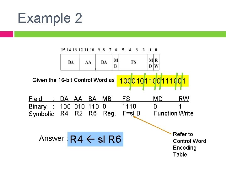
Example 2 Given the 16 -bit Control Word as 10001011001 Field : DA AA BA MB FS Binary : 100 010 110 0 1110 Symbolic : R 4 R 2 R 6 Reg. F=sl B Answer : R 4 sl R 6 MD RW 0 1 Function Write Refer to Control Word Encoding Table

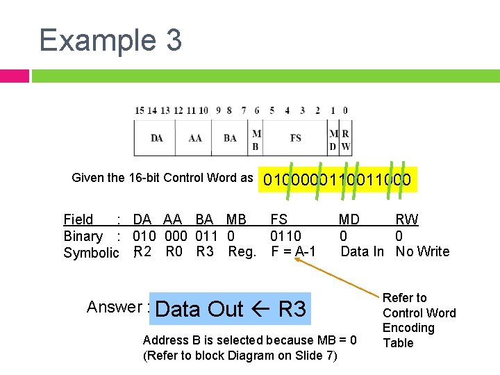
Example 3 Given the 16 -bit Control Word as 010000011000 Field : DA AA BA MB FS Binary : 010 000 0110 Symbolic : R 2 R 0 R 3 Reg. F = A-1 Answer : Data MD RW 0 0 Data In No Write Out R 3 Address B is selected because MB = 0 (Refer to block Diagram on Slide 7) Refer to Control Word Encoding Table

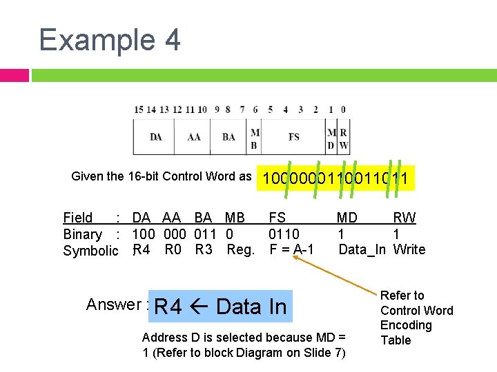
Example 4 Given the 16 -bit Control Word as 100000011011 Field : DA AA BA MB FS Binary : 100 0110 Symbolic : R 4 R 0 R 3 Reg. F = A-1 Answer : R 4 MD RW 1 1 Data_In Write Data In Address D is selected because MD = 1 (Refer to block Diagram on Slide 7) Refer to Control Word Encoding Table

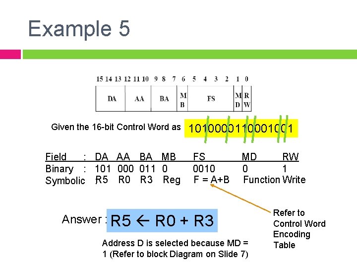
Example 5 Given the 16 -bit Control Word as Field : DA AA BA MB Binary : 101 000 011 0 Symbolic : R 5 R 0 R 3 Reg Answer : R 5 1010000110001001 FS 0010 F = A+B MD RW 0 1 Function Write R 0 + R 3 Address D is selected because MD = 1 (Refer to block Diagram on Slide 7) Refer to Control Word Encoding Table

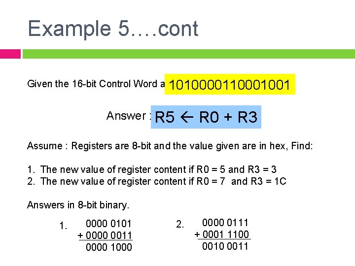
Example 5…. cont Given the 16 -bit Control Word as 1010000110001001 Answer : R 5 R 0 + R 3 Assume : Registers are 8 -bit and the value given are in hex, Find: 1. The new value of register content if R 0 = 5 and R 3 = 3 2. The new value of register content if R 0 = 7 and R 3 = 1 C Answers in 8 -bit binary. 1. 0000 0101 + 0000 0011 0000 1000 2. 0000 0111 + 0001 1100 0011

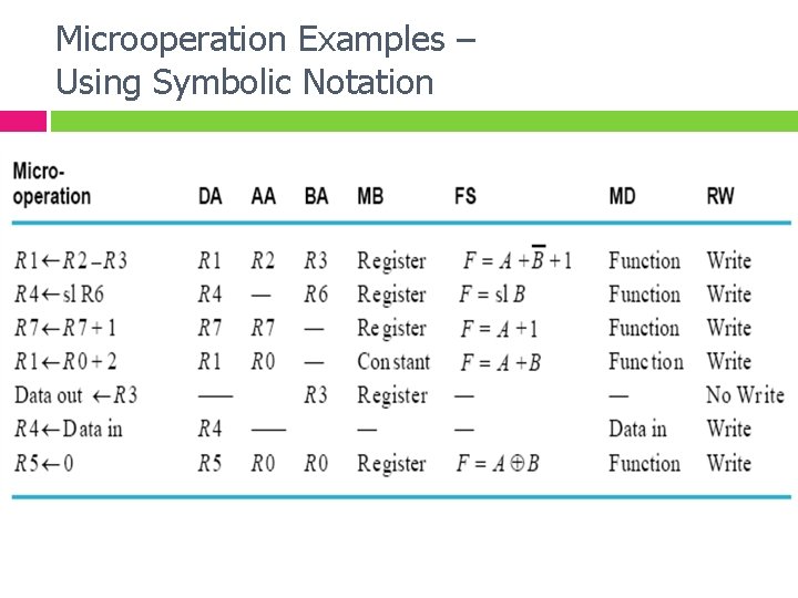
Microoperation Examples – Using Symbolic Notation

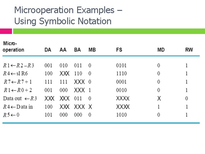
Microoperation Examples – Using Symbolic Notation

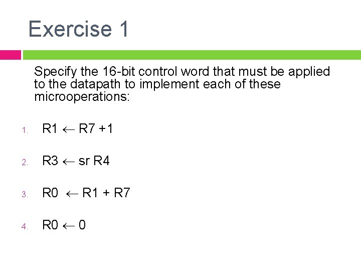
Exercise 1 Specify the 16 -bit control word that must be applied to the datapath to implement each of these microoperations: 1. R 1 R 7 +1 2. R 3 sr R 4 3. R 0 R 1 + R 7 4. R 0 0

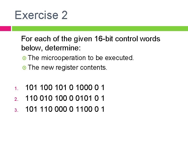
Exercise 2 For each of the given 16 -bit control words below, determine: The microoperation to be executed. The new register contents. 1. 2. 3. 101 100 101 0 1000 0 1 110 010 100 0 0101 0 1 101 110 000 0 1100 0 1

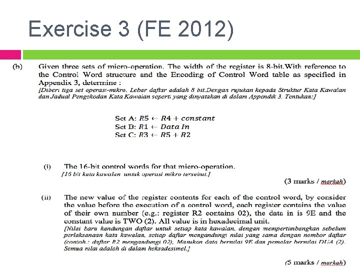
Exercise 3 (FE 2012)