EET 1093 ELECTRONIC DEVICES Introduction EET 1093 ELECTRONIC
- Slides: 15

EET 109/3 ELECTRONIC DEVICES Introduction

EET 109/3– ELECTRONIC DEVICES COURSE OUTCOME (CO) CO 1 : Ability to explain and differentiate the fundamental concepts of electronic devices. (C 4) CO 2 : Ability to analyze the basic operations of electronic devices such as diode, BJT and various types of FET. (C 4) CO 3 : Ability to design and evaluate the basic biasing circuits. (C 6, A 2, CTPS, EM, ES)

SYLLABUS Chapter 1: Semiconductor Material Atomic structure, Energy band, Conductor, Insulator, Semiconductor, Covalent bonds, Conduction in semiconductors, The p-type and n-type semiconductor, The structure of the diode, Biasing a Diode, Diode I-V characteristic, Diode Models, Testing a Diode Chapter 2: The Diode Application Half wave rectifiers, Full wave rectifiers, Power Supply Filter and Regulators, Clipper and Clamper Diode circuits, Voltage Multipliers, The Diode Datasheet and Troubleshooting.

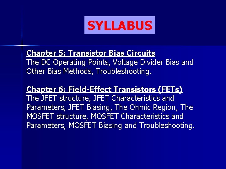
SYLLABUS Chapter 3: Special - Purpose Diodes The Zener Diode: Characteristics and application as a voltage regulator, Shockley Diode, SCR and its application, SCS, Diac, Triac, other types of diodes and Troubleshooting. Chapter 4: Bipolar Junction Transistors(BJTs) BJT structure, BJT basic operation, BJT Characteristics and Parameters, BJT as an Amplifier, BJT as a switch, The BJT Datasheet, Troubleshooting.

SYLLABUS Chapter 5: Transistor Bias Circuits The DC Operating Points, Voltage Divider Bias and Other Bias Methods, Troubleshooting. Chapter 6: Field-Effect Transistors (FETs) The JFET structure, JFET Characteristics and Parameters, JFET Biasing, The Ohmic Region, The MOSFET structure, MOSFET Characteristics and Parameters, MOSFET Biasing and Troubleshooting.

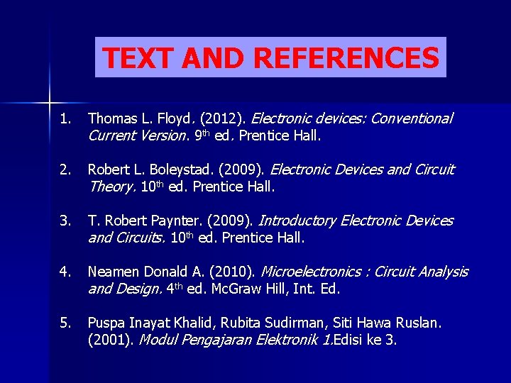
TEXT AND REFERENCES 1. Thomas L. Floyd. (2012). Electronic devices: Conventional Current Version. 9 th ed. Prentice Hall. 2. Robert L. Boleystad. (2009). Electronic Devices and Circuit Theory. 10 th ed. Prentice Hall. 3. T. Robert Paynter. (2009). Introductory Electronic Devices and Circuits. 10 th ed. Prentice Hall. 4. Neamen Donald A. (2010). Microelectronics : Circuit Analysis and Design. 4 th ed. Mc. Graw Hill, Int. Ed. 5. Puspa Inayat Khalid, Rubita Sudirman, Siti Hawa Ruslan. (2001). Modul Pengajaran Elektronik 1. Edisi ke 3.

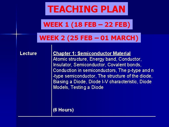
TEACHING PLAN WEEK 1 (18 FEB – 22 FEB) WEEK 2 (25 FEB – 01 MARCH) Lecture Chapter 1: Semiconductor Material Atomic structure, Energy band, Conductor, Insulator, Semiconductor, Covalent bonds, Conduction in semiconductors, The p-type and n -type semiconductor, The structure of the diode, Biasing a Diode, Diode I-V characteristic, Diode Models, Testing a Diode (6 Hours)

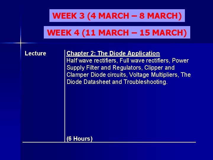
WEEK 3 (4 MARCH – 8 MARCH) WEEK 4 (11 MARCH – 15 MARCH) Lecture Chapter 2: The Diode Application Half wave rectifiers, Full wave rectifiers, Power Supply Filter and Regulators, Clipper and Clamper Diode circuits, Voltage Multipliers, The Diode Datasheet and Troubleshooting. (6 Hours)

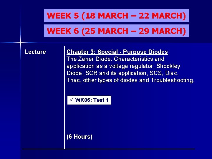
WEEK 5 (18 MARCH – 22 MARCH) WEEK 6 (25 MARCH – 29 MARCH) Lecture Chapter 3: Special - Purpose Diodes The Zener Diode: Characteristics and application as a voltage regulator, Shockley Diode, SCR and its application, SCS, Diac, Triac, other types of diodes and Troubleshooting. ü WK 06: Test 1 (6 Hours)

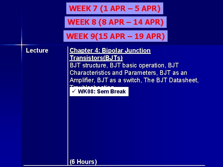
WEEK 7 (1 APR – 5 APR) WEEK 8 (8 APR – 14 APR) WEEK 9(15 APR – 19 APR) Lecture Chapter 4: Bipolar Junction Transistors(BJTs) BJT structure, BJT basic operation, BJT Characteristics and Parameters, BJT as an Amplifier, BJT as a switch, The BJT Datasheet, Troubleshooting. ü WK 08: Sem Break (6 Hours)

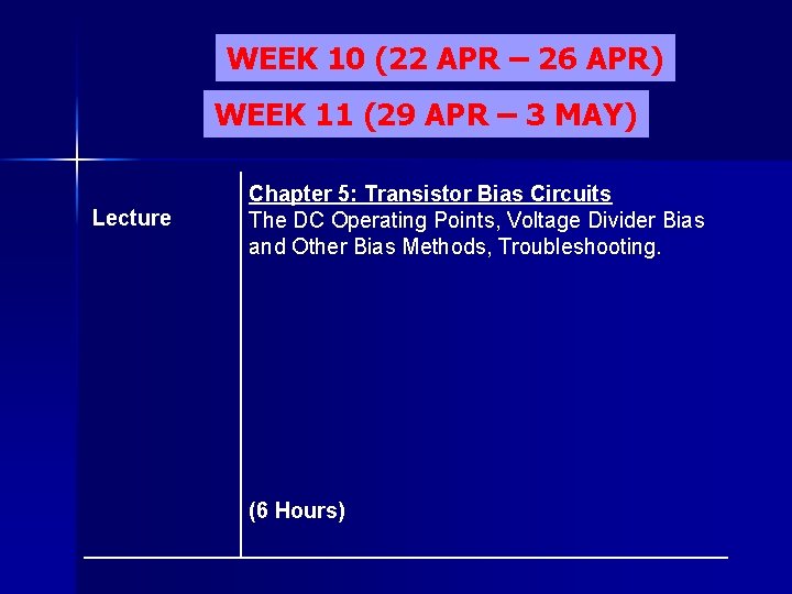
WEEK 10 (22 APR – 26 APR) WEEK 11 (29 APR – 3 MAY) Lecture Chapter 5: Transistor Bias Circuits The DC Operating Points, Voltage Divider Bias and Other Bias Methods, Troubleshooting. (6 Hours)

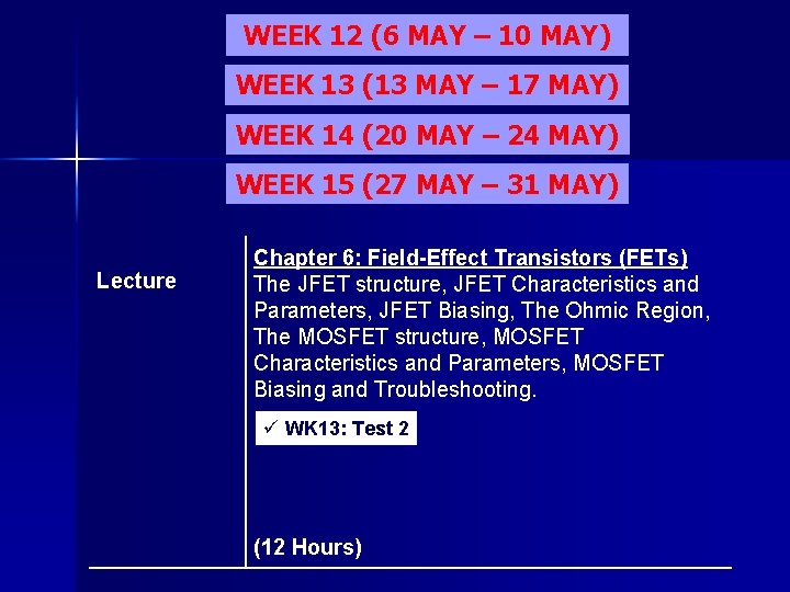
WEEK 12 (6 MAY – 10 MAY) WEEK 13 (13 MAY – 17 MAY) WEEK 14 (20 MAY – 24 MAY) WEEK 15 (27 MAY – 31 MAY) Lecture Chapter 6: Field-Effect Transistors (FETs) The JFET structure, JFET Characteristics and Parameters, JFET Biasing, The Ohmic Region, The MOSFET structure, MOSFET Characteristics and Parameters, MOSFET Biasing and Troubleshooting. ü WK 13: Test 2 (12 Hours)

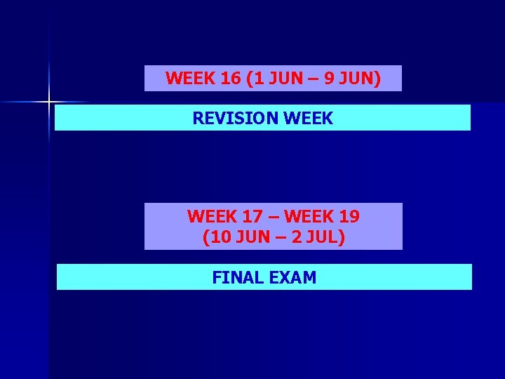
WEEK 16 (1 JUN – 9 JUN) REVISION WEEK 17 – WEEK 19 (10 JUN – 2 JUL) FINAL EXAM

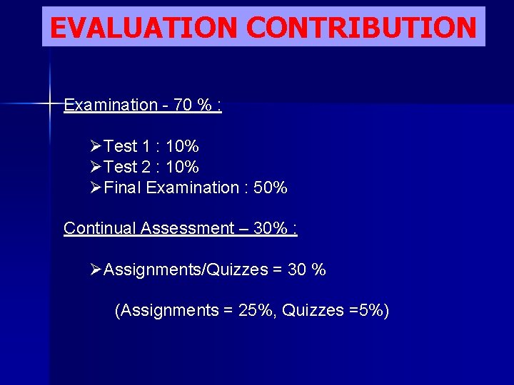
EVALUATION CONTRIBUTION Examination - 70 % : ØTest 1 : 10% ØTest 2 : 10% ØFinal Examination : 50% Continual Assessment – 30% : ØAssignments/Quizzes = 30 % (Assignments = 25%, Quizzes =5%)

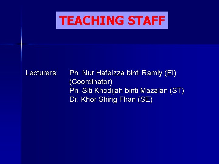
TEACHING STAFF Lecturers: Pn. Nur Hafeizza binti Ramly (EI) (Coordinator) Pn. Siti Khodijah binti Mazalan (ST) Dr. Khor Shing Fhan (SE)