Chapter 18 The 8051 Microcontroller William Kleitz Digital
- Slides: 38

Chapter 18 The 8051 Microcontroller William Kleitz Digital Electronics with VHDL, Quartus® II Version Copyright © 2006 by Pearson Education, Inc. Upper Saddle River, New Jersey 07458 All rights reserved.

Introduction • Common microprocessor components • Microprocessors designed for control applications are microcontrollers – CPU, RAM, ROM, timer/counter, and I/O ports – typical applications: • • • PC keyboard automotive sensing and engine control microwave oven VCR ATM William Kleitz Digital Electronics with VHDL, Quartus® II Version Copyright © 2006 by Pearson Education, Inc. Upper Saddle River, New Jersey 07458 All rights reserved.

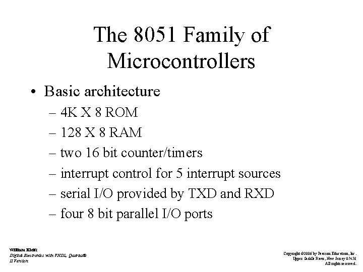
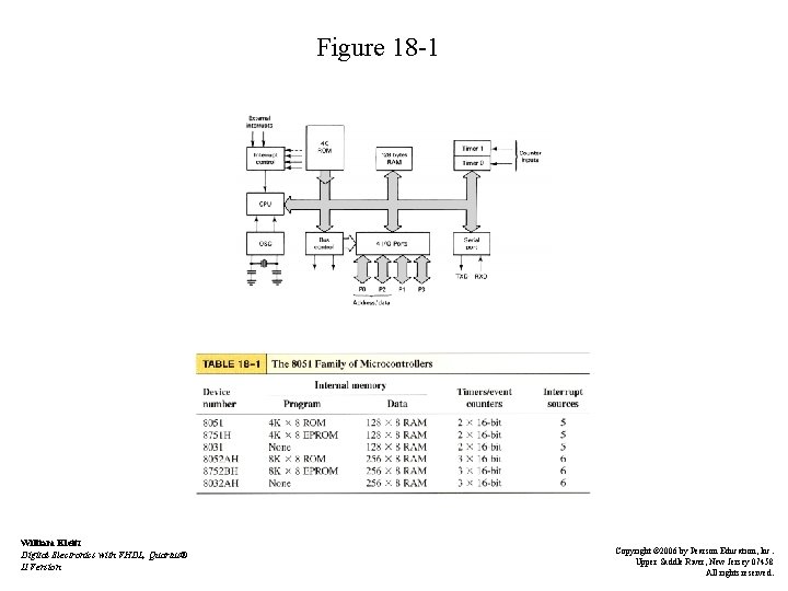
The 8051 Family of Microcontrollers • Basic architecture – 4 K X 8 ROM – 128 X 8 RAM – two 16 bit counter/timers – interrupt control for 5 interrupt sources – serial I/O provided by TXD and RXD – four 8 bit parallel I/O ports William Kleitz Digital Electronics with VHDL, Quartus® II Version Copyright © 2006 by Pearson Education, Inc. Upper Saddle River, New Jersey 07458 All rights reserved.

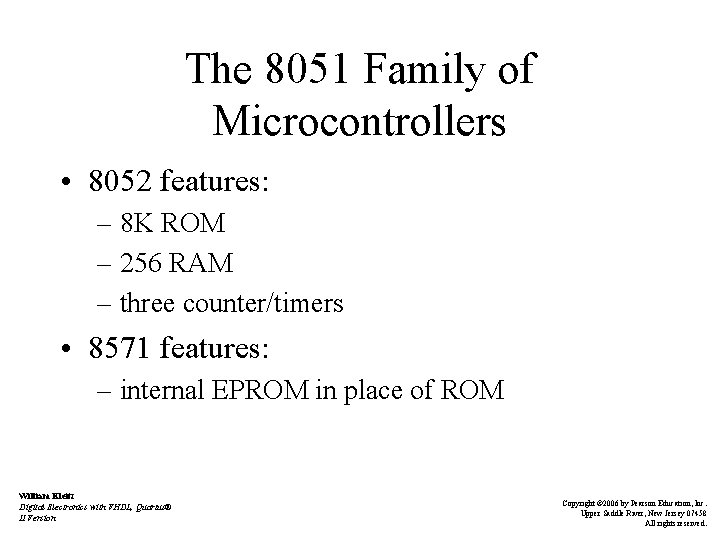
The 8051 Family of Microcontrollers • 8052 features: – 8 K ROM – 256 RAM – three counter/timers • 8571 features: – internal EPROM in place of ROM William Kleitz Digital Electronics with VHDL, Quartus® II Version Copyright © 2006 by Pearson Education, Inc. Upper Saddle River, New Jersey 07458 All rights reserved.

The 8051 Family of Microcontrollers • 8031 features: – no internal ROM (accesses external ROM or EPROM for program instructions) – See figure 18 -1 for a block diagram of the 8052 microcontroller – See table 18 -1 for a summary of 8051 family features William Kleitz Digital Electronics with VHDL, Quartus® II Version Copyright © 2006 by Pearson Education, Inc. Upper Saddle River, New Jersey 07458 All rights reserved.

Figure 18 -1 William Kleitz Digital Electronics with VHDL, Quartus® II Version Copyright © 2006 by Pearson Education, Inc. Upper Saddle River, New Jersey 07458 All rights reserved.

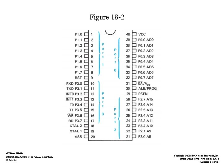
8051 Architecture • The same internal address space and external pins must be used for multiple functions • Similar to 8085 A for multiplexed lines • See figure 18 -2 for pin configuration William Kleitz Digital Electronics with VHDL, Quartus® II Version Copyright © 2006 by Pearson Education, Inc. Upper Saddle River, New Jersey 07458 All rights reserved.

Figure 18 -2 William Kleitz Digital Electronics with VHDL, Quartus® II Version Copyright © 2006 by Pearson Education, Inc. Upper Saddle River, New Jersey 07458 All rights reserved.

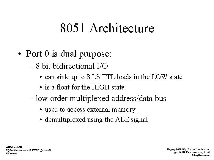
8051 Architecture • Port 0 is dual purpose: – 8 bit bidirectional I/O • can sink up to 8 LS TTL loads in the LOW state • is a float for the HIGH state – low order multiplexed address/data bus • used to access external memory • demultiplexed using the ALE signal William Kleitz Digital Electronics with VHDL, Quartus® II Version Copyright © 2006 by Pearson Education, Inc. Upper Saddle River, New Jersey 07458 All rights reserved.

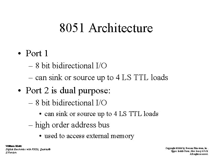
8051 Architecture • Port 1 – 8 bit bidirectional I/O – can sink or source up to 4 LS TTL loads • Port 2 is dual purpose: – 8 bit bidirectional I/O • can sink or source up to 4 LS TTL loads – high order address bus • used to access external memory William Kleitz Digital Electronics with VHDL, Quartus® II Version Copyright © 2006 by Pearson Education, Inc. Upper Saddle River, New Jersey 07458 All rights reserved.

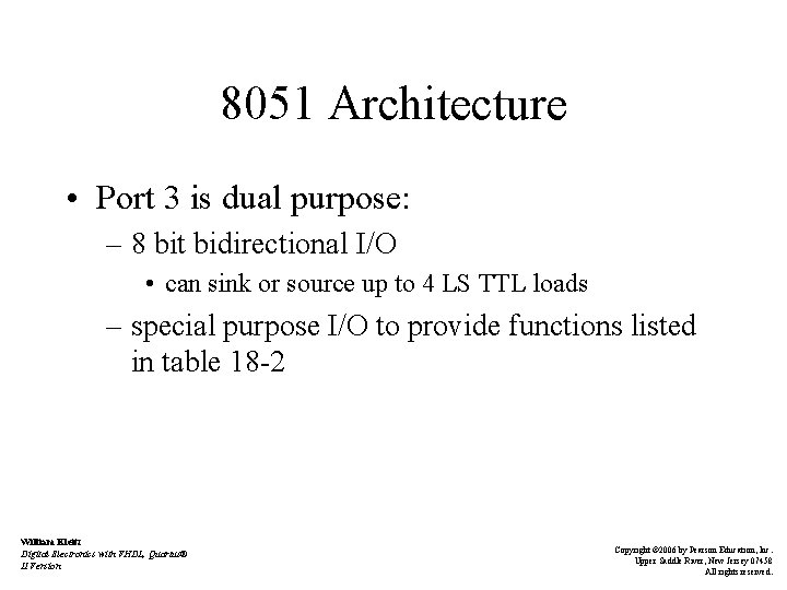
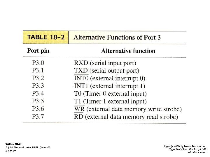
8051 Architecture • Port 3 is dual purpose: – 8 bit bidirectional I/O • can sink or source up to 4 LS TTL loads – special purpose I/O to provide functions listed in table 18 -2 William Kleitz Digital Electronics with VHDL, Quartus® II Version Copyright © 2006 by Pearson Education, Inc. Upper Saddle River, New Jersey 07458 All rights reserved.

William Kleitz Digital Electronics with VHDL, Quartus® II Version Copyright © 2006 by Pearson Education, Inc. Upper Saddle River, New Jersey 07458 All rights reserved.

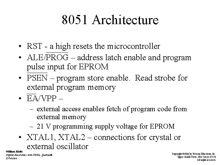
8051 Architecture • RST - a high resets the microcontroller • ALE/PROG – address latch enable and program pulse input for EPROM • PSEN – program store enable. Read strobe for external program memory • EA/VPP – – external access enables fetch of program code from external memory – 21 V programming supply voltage for EPROM • XTAL 1, XTAL 2 – connections for crystal or external oscillator William Kleitz Digital Electronics with VHDL, Quartus® II Version Copyright © 2006 by Pearson Education, Inc. Upper Saddle River, New Jersey 07458 All rights reserved.

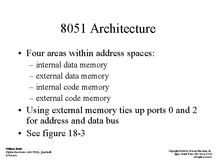
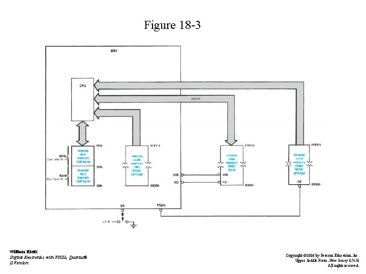
8051 Architecture • Four areas within address spaces: – internal data memory – external data memory – internal code memory – external code memory • Using external memory ties up ports 0 and 2 for address and data bus • See figure 18 -3 William Kleitz Digital Electronics with VHDL, Quartus® II Version Copyright © 2006 by Pearson Education, Inc. Upper Saddle River, New Jersey 07458 All rights reserved.

Figure 18 -3 William Kleitz Digital Electronics with VHDL, Quartus® II Version Copyright © 2006 by Pearson Education, Inc. Upper Saddle River, New Jersey 07458 All rights reserved.

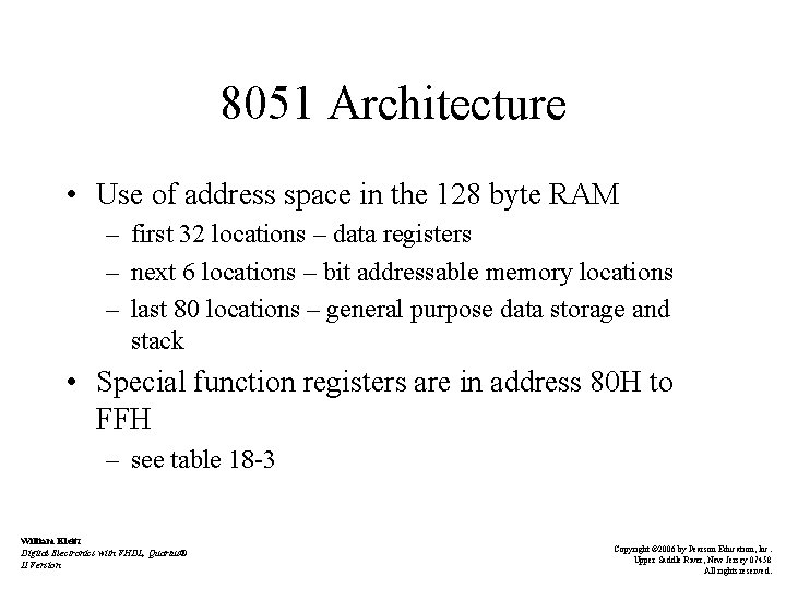
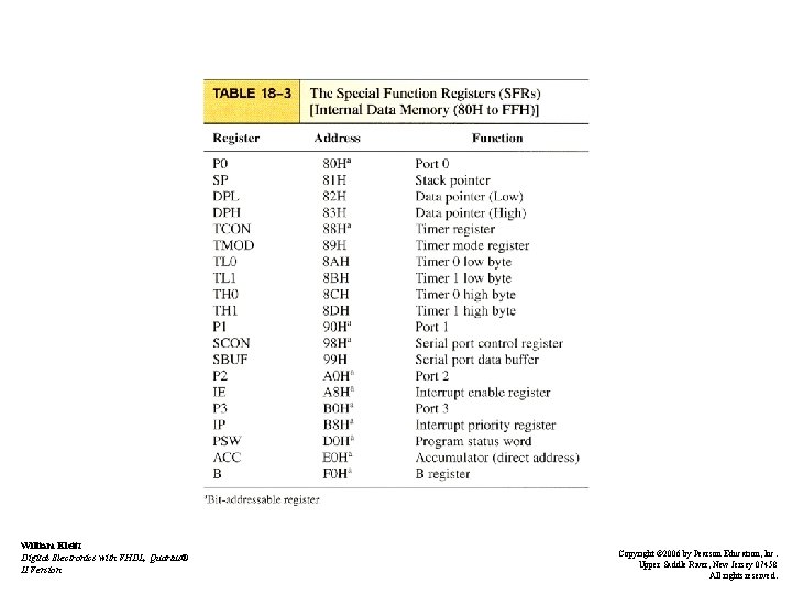
8051 Architecture • Use of address space in the 128 byte RAM – first 32 locations – data registers – next 6 locations – bit addressable memory locations – last 80 locations – general purpose data storage and stack • Special function registers are in address 80 H to FFH – see table 18 -3 William Kleitz Digital Electronics with VHDL, Quartus® II Version Copyright © 2006 by Pearson Education, Inc. Upper Saddle River, New Jersey 07458 All rights reserved.

William Kleitz Digital Electronics with VHDL, Quartus® II Version Copyright © 2006 by Pearson Education, Inc. Upper Saddle River, New Jersey 07458 All rights reserved.

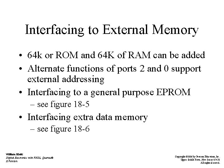
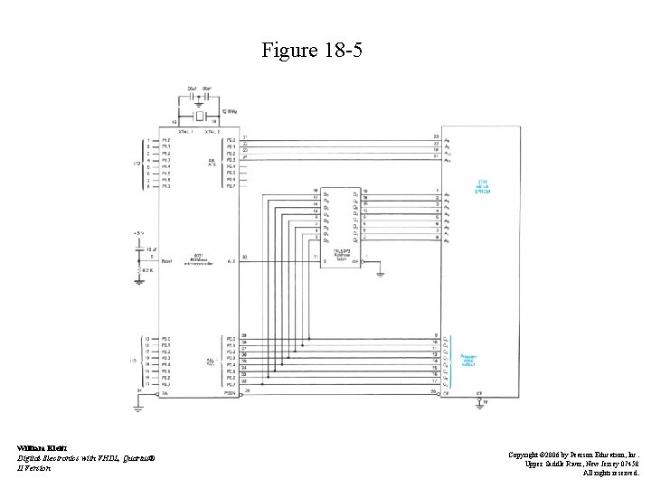
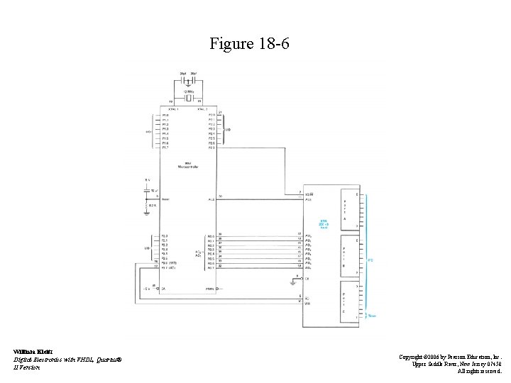
Interfacing to External Memory • 64 k or ROM and 64 K of RAM can be added • Alternate functions of ports 2 and 0 support external addressing • Interfacing to a general purpose EPROM – see figure 18 -5 • Interfacing extra data memory – see figure 18 -6 William Kleitz Digital Electronics with VHDL, Quartus® II Version Copyright © 2006 by Pearson Education, Inc. Upper Saddle River, New Jersey 07458 All rights reserved.

Figure 18 -5 William Kleitz Digital Electronics with VHDL, Quartus® II Version Copyright © 2006 by Pearson Education, Inc. Upper Saddle River, New Jersey 07458 All rights reserved.

Figure 18 -6 William Kleitz Digital Electronics with VHDL, Quartus® II Version Copyright © 2006 by Pearson Education, Inc. Upper Saddle River, New Jersey 07458 All rights reserved.

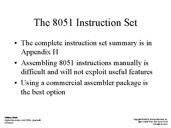
The 8051 Instruction Set • The complete instruction set summary is in Appendix H • Assembling 8051 instructions manually is difficult and will not exploit useful features • Using a commercial assembler package is the best option William Kleitz Digital Electronics with VHDL, Quartus® II Version Copyright © 2006 by Pearson Education, Inc. Upper Saddle River, New Jersey 07458 All rights reserved.

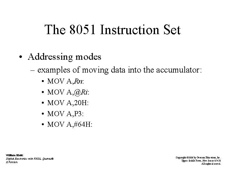
The 8051 Instruction Set • Addressing modes – examples of moving data into the accumulator: • • • MOV A, Rn: MOV A, @Ri: MOV A, 20 H: MOV A, P 3: MOV A, #64 H: William Kleitz Digital Electronics with VHDL, Quartus® II Version Copyright © 2006 by Pearson Education, Inc. Upper Saddle River, New Jersey 07458 All rights reserved.

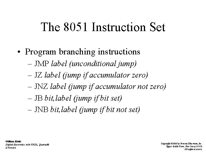
The 8051 Instruction Set • Program branching instructions – JMP label (unconditional jump) – JZ label (jump if accumulator zero) – JNZ label (jump if accumulator not zero) – JB bit, label (jump if bit set) – JNB bit, label (jump if bit not set) William Kleitz Digital Electronics with VHDL, Quartus® II Version Copyright © 2006 by Pearson Education, Inc. Upper Saddle River, New Jersey 07458 All rights reserved.

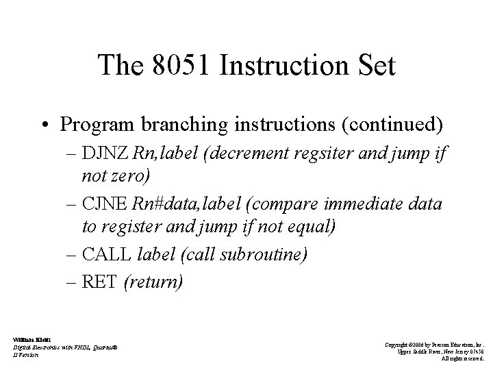
The 8051 Instruction Set • Program branching instructions (continued) – DJNZ Rn, label (decrement regsiter and jump if not zero) – CJNE Rn#data, label (compare immediate data to register and jump if not equal) – CALL label (call subroutine) – RET (return) William Kleitz Digital Electronics with VHDL, Quartus® II Version Copyright © 2006 by Pearson Education, Inc. Upper Saddle River, New Jersey 07458 All rights reserved.

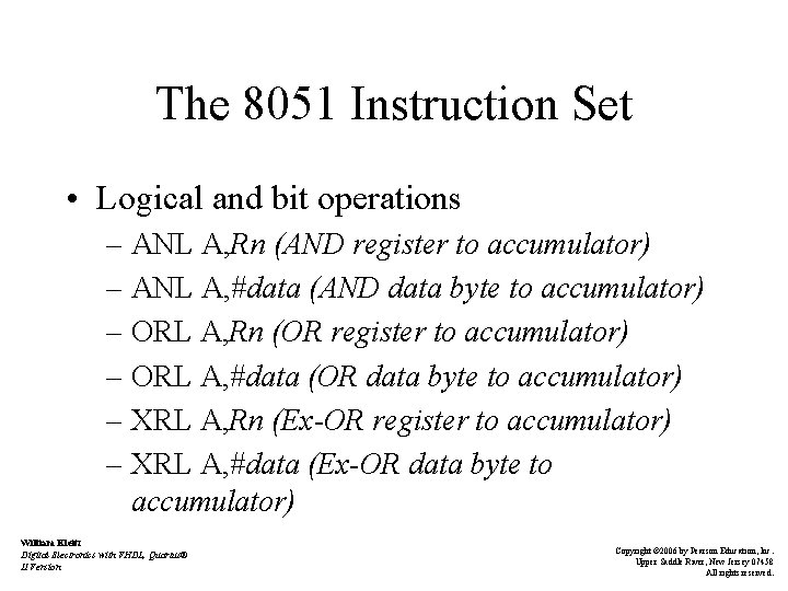
The 8051 Instruction Set • Logical and bit operations – ANL A, Rn (AND register to accumulator) – ANL A, #data (AND data byte to accumulator) – ORL A, Rn (OR register to accumulator) – ORL A, #data (OR data byte to accumulator) – XRL A, Rn (Ex-OR register to accumulator) – XRL A, #data (Ex-OR data byte to accumulator) William Kleitz Digital Electronics with VHDL, Quartus® II Version Copyright © 2006 by Pearson Education, Inc. Upper Saddle River, New Jersey 07458 All rights reserved.

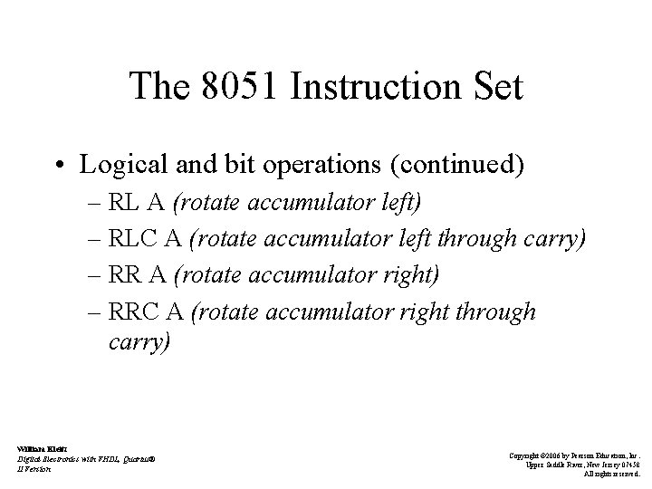
The 8051 Instruction Set • Logical and bit operations (continued) – RL A (rotate accumulator left) – RLC A (rotate accumulator left through carry) – RR A (rotate accumulator right) – RRC A (rotate accumulator right through carry) William Kleitz Digital Electronics with VHDL, Quartus® II Version Copyright © 2006 by Pearson Education, Inc. Upper Saddle River, New Jersey 07458 All rights reserved.

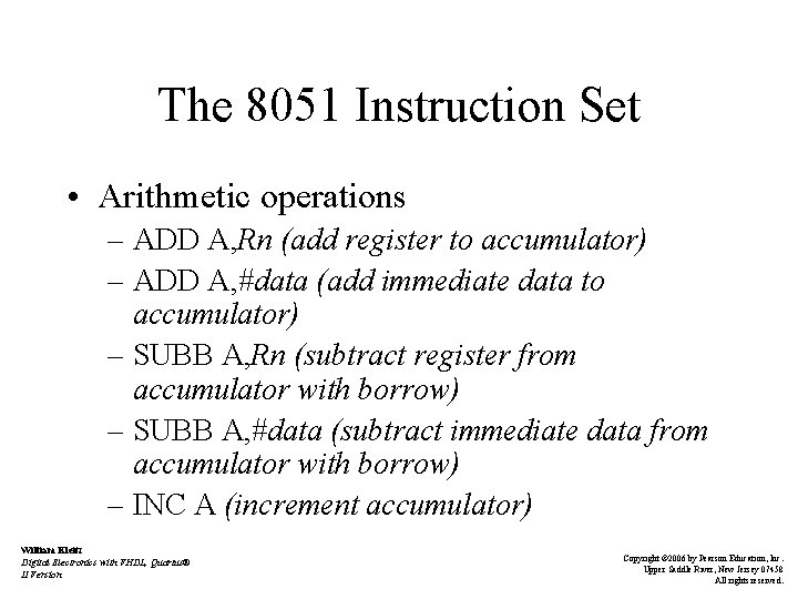
The 8051 Instruction Set • Arithmetic operations – ADD A, Rn (add register to accumulator) – ADD A, #data (add immediate data to accumulator) – SUBB A, Rn (subtract register from accumulator with borrow) – SUBB A, #data (subtract immediate data from accumulator with borrow) – INC A (increment accumulator) William Kleitz Digital Electronics with VHDL, Quartus® II Version Copyright © 2006 by Pearson Education, Inc. Upper Saddle River, New Jersey 07458 All rights reserved.

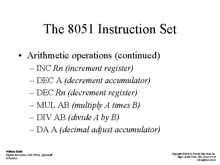
The 8051 Instruction Set • Arithmetic operations (continued) – INC Rn (increment register) – DEC A (decrement accumulator) – DEC Rn (decrement register) – MUL AB (multiply A times B) – DIV AB (divide A by B) – DA A (decimal adjust accumulator) William Kleitz Digital Electronics with VHDL, Quartus® II Version Copyright © 2006 by Pearson Education, Inc. Upper Saddle River, New Jersey 07458 All rights reserved.

8051 Applications • Bit handling instructions and built in I/O makes the 8051 useful for data acquisition and control applications – instruction timing – time delay • See examples 18 -11, 18 -12, and 18 -13 William Kleitz Digital Electronics with VHDL, Quartus® II Version Copyright © 2006 by Pearson Education, Inc. Upper Saddle River, New Jersey 07458 All rights reserved.

Data Acquisition and Control System Application • The 8051 microcontroller module – 8051 microcontroller – I/O buffers – address latch – EPROM interface • The ADC interface module – ADC 0804 IC William Kleitz Digital Electronics with VHDL, Quartus® II Version Copyright © 2006 by Pearson Education, Inc. Upper Saddle River, New Jersey 07458 All rights reserved.

Data Acquisition and Control System Application • The DAC interface module – MC 1408 • Applications – centigrade thermometer – temperature dependent PWM speed control – integrating solar radiometer William Kleitz Digital Electronics with VHDL, Quartus® II Version Copyright © 2006 by Pearson Education, Inc. Upper Saddle River, New Jersey 07458 All rights reserved.

Summary • The 8051 microcontroller is different from a microprocessor because it has the CPU, ROM, RAM, timer/counter, and parallel and serial ports fabricated into a single IC. • Thirty two of the forty pins of the 8051 are used for the four 8 bit parallel I/O ports. Three of the ports share their function with the address, data, and control buses. William Kleitz Digital Electronics with VHDL, Quartus® II Version Copyright © 2006 by Pearson Education, Inc. Upper Saddle River, New Jersey 07458 All rights reserved.

Summary • The address spaces of the 8051 are divided into four distinct areas: internal data memory, external data memory, internal code memory, and external code memory. The internal data memory is further divided into user RAM and special function registers (SFRs). William Kleitz Digital Electronics with VHDL, Quartus® II Version Copyright © 2006 by Pearson Education, Inc. Upper Saddle River, New Jersey 07458 All rights reserved.

Summary • To interface to an external EPROM like the 2732, an octal D latch is required to demultiplex the address/data bus, which is shared with port 0. The external access (EA) pin is tied LOW and the (PSEN) output is used to enable the output of the EPROM. William Kleitz Digital Electronics with VHDL, Quartus® II Version Copyright © 2006 by Pearson Education, Inc. Upper Saddle River, New Jersey 07458 All rights reserved.

Summary • Extra data memory and I/O ports can be interfaced by using the 8155 IC. The 8155 demultiplexes the address/data bus internally so an octal D latch is not required. • The MOV instruction is very powerful, providing the ability to move data almost anywhere internal or external to the microcontroller and to the I/O ports. William Kleitz Digital Electronics with VHDL, Quartus® II Version Copyright © 2006 by Pearson Education, Inc. Upper Saddle River, New Jersey 07458 All rights reserved.

Summary • Program branching is accomplished by use of many different conditional and unconditional jumps and calls. • The 8051 instruction set provides the ability to work with individual bits, which makes it very efficient for on/off control operation. Instructions are available for all the logic functions, rotates, and bit manipulations. William Kleitz Digital Electronics with VHDL, Quartus® II Version Copyright © 2006 by Pearson Education, Inc. Upper Saddle River, New Jersey 07458 All rights reserved.

Summary • Instructions are provided for all the basic arithmetic instructions: addition, subtraction, multiplication, division, incrementing, and decrementing. • Each instruction machine cycle takes 12 clock periods to complete. This means that if a 2 MHz crystal is used, each machine cycle takes microsecond to complete. One complete instruction takes 1, 2, or 4 machine cycles. William Kleitz Digital Electronics with VHDL, Quartus® II Version Copyright © 2006 by Pearson Education, Inc. Upper Saddle River, New Jersey 07458 All rights reserved.

Summary • A 4 by 4 matrix keyboard can be scanned using bit operations on a single I/O port. • Interfacing an 8 bit analog to digital converter to an 8051 is accomplished with one port and two bits on a second port. The start-conversion LOW pulse is issued with bit setting instructions and the end-of-conversion signal is monitored with bit checking instructions. William Kleitz Digital Electronics with VHDL, Quartus® II Version Copyright © 2006 by Pearson Education, Inc. Upper Saddle River, New Jersey 07458 All rights reserved.