UNITII Sheet Resistance Rs IC resistors have a
- Slides: 110

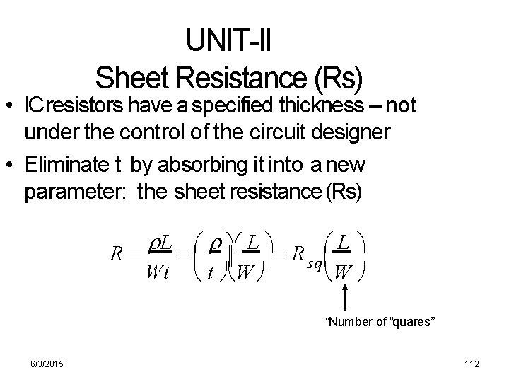
UNIT-II Sheet Resistance (Rs) • IC resistors have a specified thickness – not under the control of the circuit designer • Eliminate t by absorbing it into a new parameter: the sheet resistance (Rs) R L Wt t W W sq “Number of “quares” 6/3/2015 112

BASICELECTRICALPROPERTIES Topics • Basic electrical properties of MOS and Bi. CMOS circuits: • Ids-Vds relationships • MOS transistor threshold voltage, gm, gds • figure of merit wo • pass transistor • NMOS inverter • Various pull-ups • CMOS inverter analysis and design • Bi. CMOS inverters 6/3/2015 129

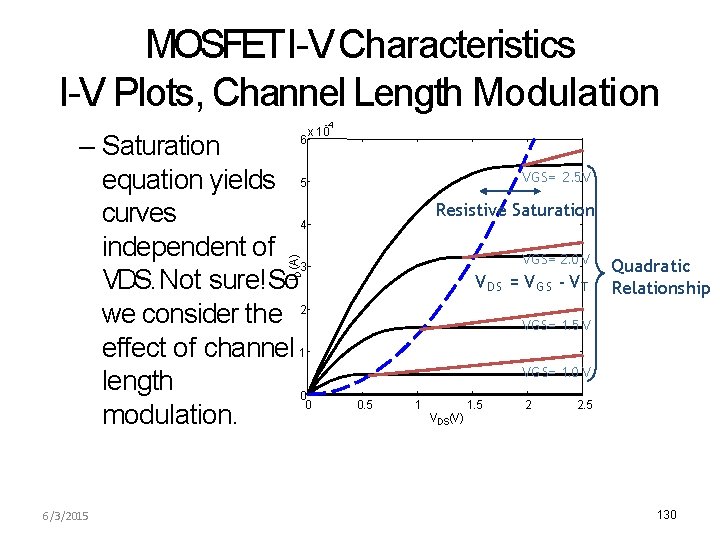
MOSFETI-V Characteristics I-V Plots, Channel Length Modulation -4 x 10 VGS= 2. 5 V Resistive Saturation VGS= 2. 0 V ID (A) 6 – Saturation equation yields 5 curves 4 independent of 3 VDS. Not sure! So we consider the 2 effect of channel 1 length 0 0 modulation. 6/3/2015 VD S = VG S - VT Quadratic Relationship VGS= 1. 5 V VGS= 1. 0 V 0. 5 1 1. 5 VDS(V) 2 2. 5 130

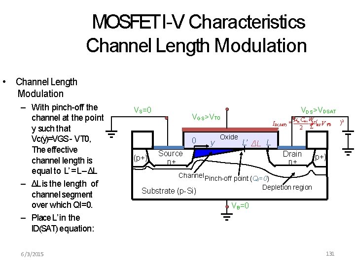
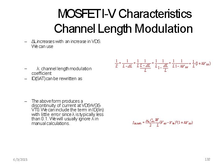
MOSFETI-V Characteristics Channel Length Modulation • Channel Length Modulation – With pinch-off the channel at the point y such that Vc(y)=VGS - VT 0, The effective channel length is equal to L’ = L– ΔL is the length of channel segment over which QI=0. – Place L’ in the ID(SAT) equation: 6/3/2015 VS=0 0 (p+) VDS>VDSAT VGS>VT 0 y I D ( SAT ) Oxide n Cox W ( V GS V T 0 2 L L’ ΔL L Source n+ Drain n+ (p+) Channel Pinch-off point (QI=0) Depletion region Substrate (p-Si) VB=0 131 )2

MOSFETI-V Characteristics Channel Length Modulation – ΔL increases with an increase in VDS. We can use – λ: channel length modulation coefficient – ID(SAT) can be rewritten as – The above form produces a discontinuity of current at VDS=VGSVT 0. We can include the term in ID(lin) with little error since λ is typically less than 0. 1. We will usually ignore λ in manual calculations. 6/3/2015 1 1 1 1 1 1 V DS ΔL L' L ΔL L L 1 V DS L L L I D ( SAT ) n Cox W ( V GS V T 0 )2 (1 V DS ) 2 L 132

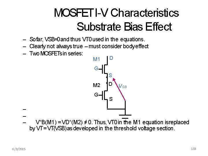
MOSFETI-V Characteristics Substrate Bias Effect – So far, VSB=0 and thus VT 0 used in the equations. – Clearly not always true – must consider body effect – Two MOSFETsin series: M 1 D G S M 2 G – – – 6/3/2015 D VSB S V“B(M 1) = VD“(M 2) ≠ 0. Thus, VT 0 in the M 1 equation isreplaced by VT = VT(VSB) as developed in the threshold voltage section. 133

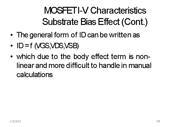
MOSFETI-V Characteristics Substrate Bias Effect (Cont. ) • The general form of ID can be written as • ID = f (VGS, VDS, VSB) • which due to the body effect term is nonlinear and more difficult to handle in manual calculations 6/3/2015 134

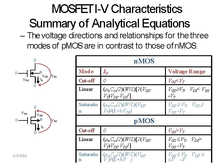
MOSFETI-V Characteristics Summary of Analytical Equations – The voltage directions and relationships for the three modes of p. MOS are in contrast to those of n. MOS D B G VSB VDS ID VGS S VSB B G ID D 6/3/2015 ID Voltage Range Cut-off 0 VGS<VT Linear (µn. Cox/2)(W/L)[2(VGSVT)VDS-VDS 2] VGS VT,VDS< VGS -VT Saturatio (µn. Cox/2)(W/L)(VGSn VT)2(1+h. VDS) S VGS Mode VGS VT,VDS VGS -VT p. MOS VDS Cut-off 0 VGS>VT Linear (µn. Cox/2)(W/L)[2(VGSVT)VDS-VDS 2] VGS VT,VDS> VGS -VT Saturatio (µn. Cox/2)(W/L)(VGSn V )2(1+h. V ) VGS VT,VDS 135 V -V

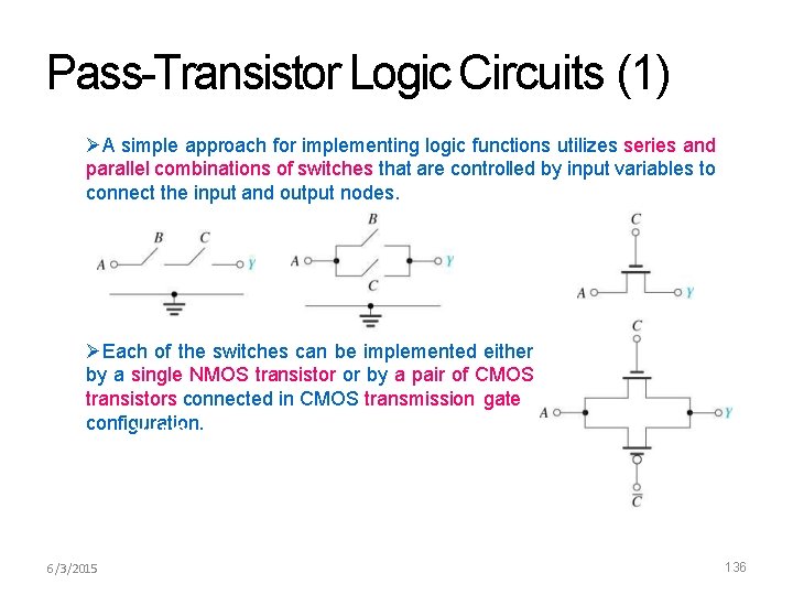
Pass-Transistor Logic Circuits (1) A simple approach for implementing logic functions utilizes series and parallel combinations of switches that are controlled by input variables to connect the input and output nodes. Each of the switches can be implemented either by a single NMOS transistor or by a pair of CMOS transistors connected in CMOS transmission gate configuration. Y=AC 6/3/2015 136

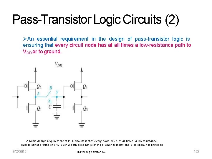
Pass-Transistor Logic Circuits (2) An essential requirement in the design of pass-transistor logic is ensuring that every circuit node has at all times a low-resistance path to VDD or to ground. A basic design requirement of PTL circuits is that every node have, at all times, a low resistance path to either ground or VDD. Such a path does not exist in (a) when B is low and S 1 is open. It is provided in 6/3/2015 (b) through switch S 2. 137

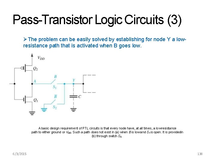
Pass-Transistor Logic Circuits (3) The problem can be easily solved by establishing for node Y a lowresistance path that is activated when B goes low. A basic design requirement of PTL circuits is that every node have, at all times, a low resistance path to either ground or VDD. Such a path does not exist in (a) when B is low and S 1 is open. It is providedin (b) through switch S 2. 6/3/2015 138

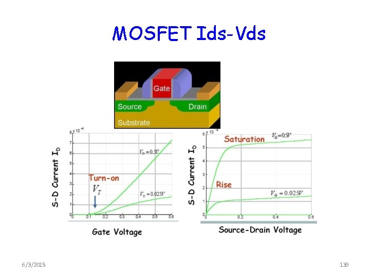
MOSFET Ids-Vds 6/3/2015 139

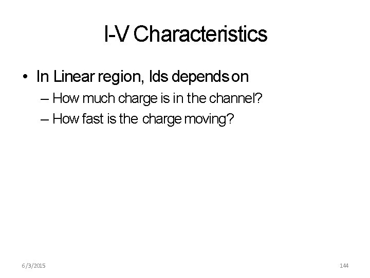
I-V Characteristics • In Linear region, Ids depends on – How much charge is in the channel? – How fast is the charge moving? 6/3/2015 144

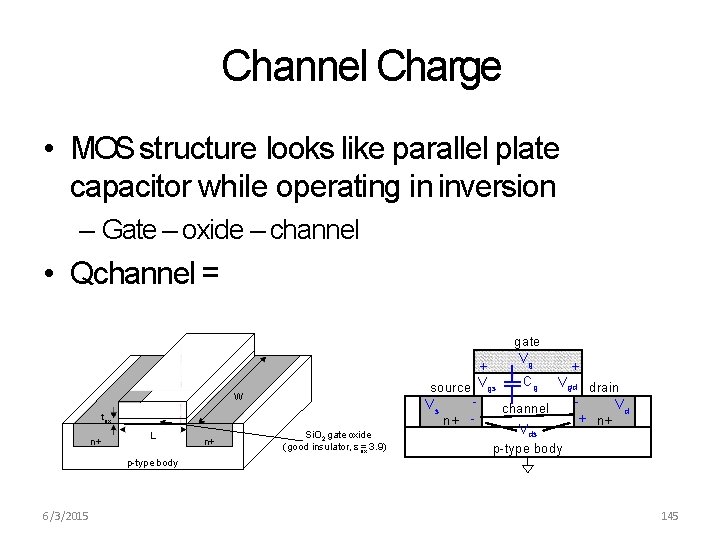
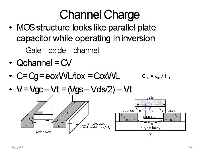
Channel Charge • MOS structure looks like parallel plate capacitor while operating in inversion – Gate – oxide – channel • Qchannel = gate Vg polysilicon gate W tox n+ L n+ Si. O 2 gate oxide (good insulator, ox = 3. 9) + + Cg Vgd drain source Vgs Vs Vd channel + n+ n+ Vds p-type body 6/3/2015 145

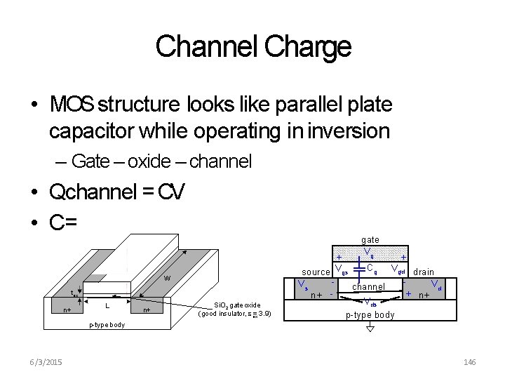
Channel Charge • MOS structure looks like parallel plate capacitor while operating in inversion – Gate – oxide – channel • Qchannel = CV • C= gate Vg polysilicon gate W tox n+ L n+ Si. O 2 gate oxide (good insulator, ox = 3. 9) + + Cg Vgd drain source Vgs Vs Vd channel + n+ n+ Vds p-type body 6/3/2015 146

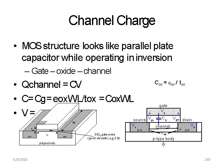
Channel Charge • MOS structure looks like parallel plate capacitor while operating in inversion – Gate – oxide – channel • Qchannel = CV • C= Cg= eox. WL/tox = Cox. WL + • V= source V polysilicon gate W Vs tox n+ L n+ Si. O 2 gate oxide (good insulator, ox = 3. 9) n+ - Cox = ox / tox gate Vg + Cg Vgd drain Vd channel + n+ Vds p-type body gs p-type body 6/3/2015 147

Channel Charge • MOS structure looks like parallel plate capacitor while operating in inversion – Gate – oxide – channel • Qchannel = CV • C= Cg= eox. WL/tox = Cox. WL • V = Vgc – Vt = (Vgs – Vds/2) – Vt gate Vg polysilicon gate W tox n+ L n+ Cox = ox / tox Si. O 2 gate oxide (good insulator, ox = 3. 9) + + Cg Vgd drain source Vgs Vs Vd channel + n+ n+ Vds p-type body 6/3/2015 148

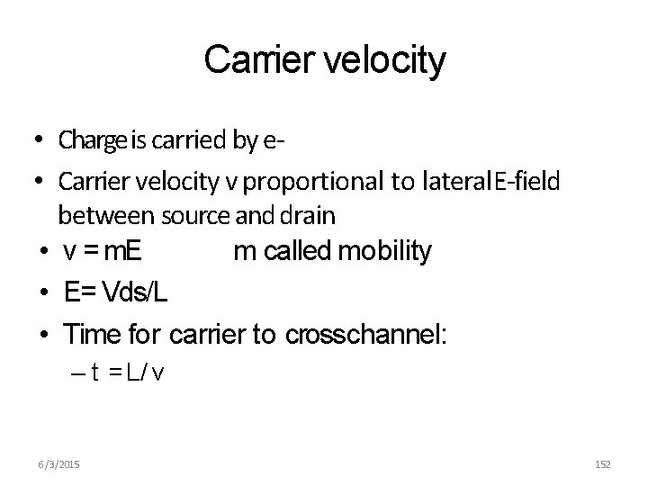
Carrier velocity • Charge is carried by e • Carrier velocity v proportional to lateral E-field between source and drain 6/3/2015 149

Carrier velocity • Charge is carried by e • Carrier velocity v proportional to lateral E-field between source and drain • v = m. E m called mobility • E=energy 6/3/2015 150

Carrier velocity • Charge is carried by e • Carrier velocity v proportional to lateral E-field between source and drain m called mobility • v = m. E • E= Vds/L • Time for carrier to crosschannel: –t= 6/3/2015 151

Carrier velocity • Charge is carried by e • Carrier velocity v proportional to lateral E-field between source and drain m called mobility • v = m. E • E= Vds/L • Time for carrier to crosschannel: – t = L/ v 6/3/2015 152

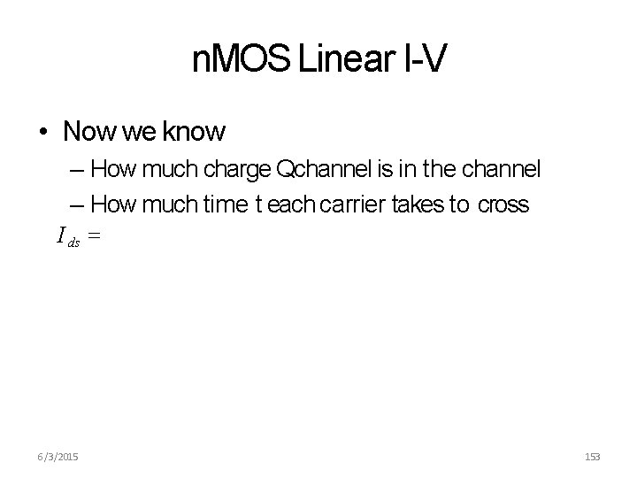
n. MOS Linear I-V • Now we know – How much charge Qchannel is in the channel – How much time t each carrier takes to cross I ds 6/3/2015 153

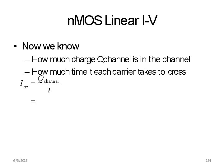
n. MOS Linear I-V • Now we know – How much charge Qchannel is in the channel – How much time t each carrier takes to cross I ds Qchannel t 6/3/2015 154

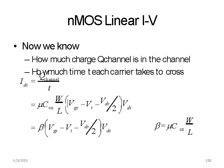
n. MOS Linear I-V • Now we know – How much charge Qchannel is in the channel – Ho. Qwmuch time t each carrier takes to cross I ds channel t W C ox V gs Vt Vds 2 Vds L W V = C ox Vgs Vt ds 2 Vds L 6/3/2015 155

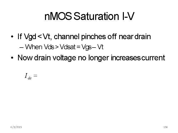
n. MOS Saturation I-V • If Vgd < Vt, channel pinches off near drain – When Vds > Vdsat = Vgs – Vt • Now drain voltage no longer increases current I ds 6/3/2015 156

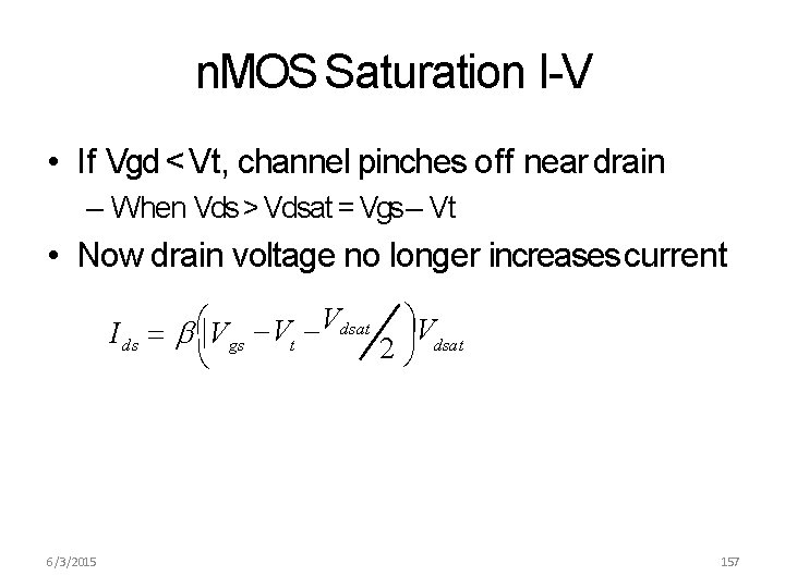
n. MOS Saturation I-V • If Vgd < Vt, channel pinches off near drain – When Vds > Vdsat = Vgs – Vt • Now drain voltage no longer increases current I ds V gs Vt Vdsat 2 6/3/2015 157

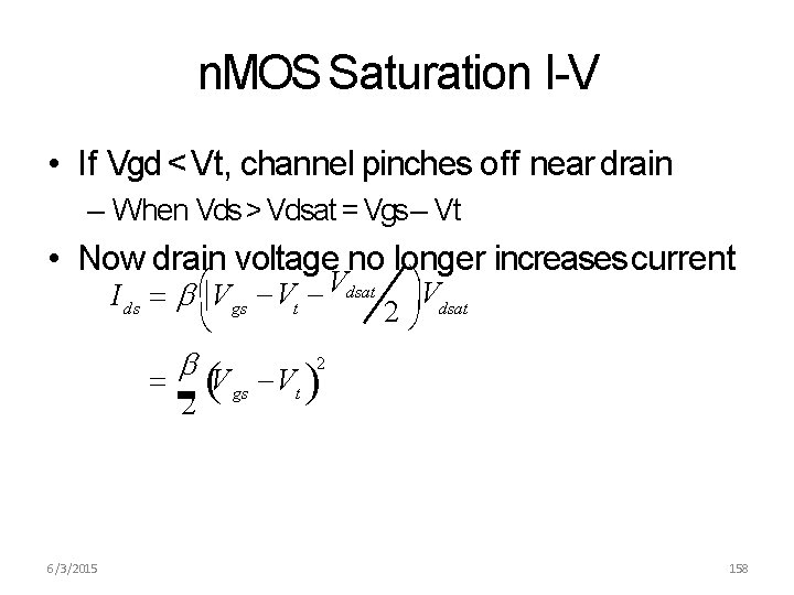
n. MOS Saturation I-V • If Vgd < Vt, channel pinches off near drain – When Vds > Vdsat = Vgs – Vt • Now drain voltage no longer increases current I ds V gs Vt Vdsat 2 2 V gs Vt 2 6/3/2015 158

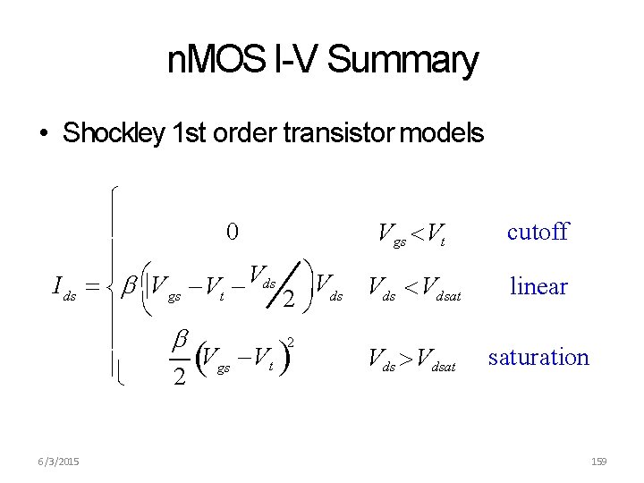
n. MOS I-V Summary • Shockley 1 st order transistor models 0 Vgs Vt I ds V gs Vt Vds Vdsat 2 2 Vgs Vt Vdsat 2 6/3/2015 cutoff linear saturation 159

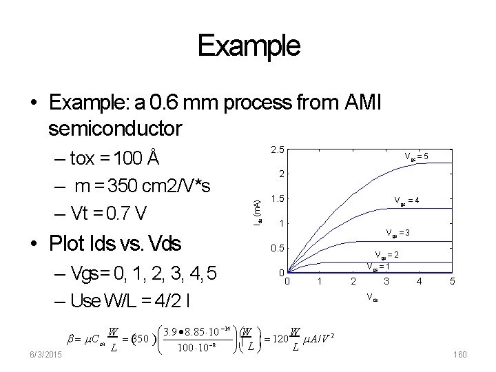
Example • Example: a 0. 6 mm process from AMI semiconductor • Plot Ids vs. Vds – Vgs = 0, 1, 2, 3, 4, 5 – Use W/L = 4/2 l 6/3/2015 Vgs = 5 2 Ids (m. A) – tox = 100 Å – m = 350 cm 2/V*s – Vt = 0. 7 V 2. 5 1. 5 Vgs = 4 1 Vgs = 3 0. 5 0 0 Vgs = 2 Vgs = 1 1 W 3. 9 8. 85 10 14 W W C ox 350 A /V 2 120 8 L L L 100 10 2 3 4 5 Vds 160

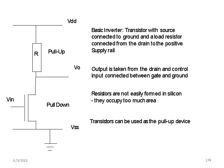
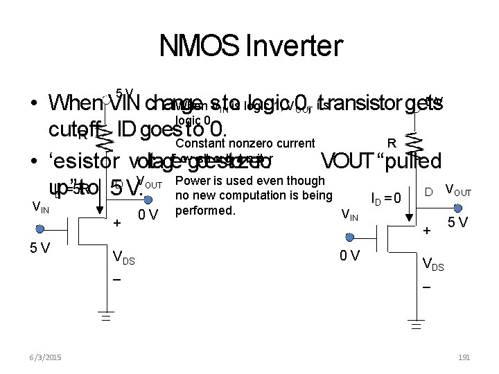
Vdd R Basic Inverter: Transistor with source connected to ground a load resistor connected from the drain to the positive Supply rail Pull-Up Vo Vin Resistors are not easily formed in silicon - they occupy too much area Pull Down Vss 6/3/2015 Output is taken from the drain and control input connected between gate and ground Transistors can be used as the pull-up device 174

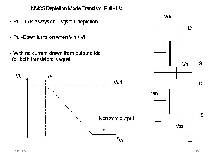
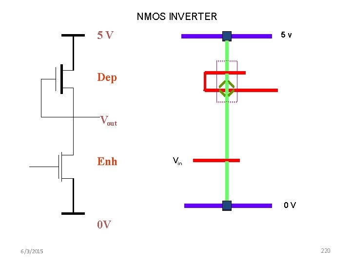
NMOS Depletion Mode Transistor Pull - Up Vdd • Pull-Up is always on – Vgs = 0; depletion D • Pull-Down turns on when Vin > Vt • With no current drawn from outputs, Ids for both transistors is equal V 0 Vt Vo Vdd S D Vin S Non-zero output Vss Vi 6/3/2015 175

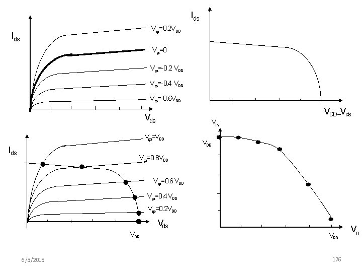
Ids Vgs=0. 2 VDD Ids Vgs=0 Vgs=-0. 2 VDD Vgs=-0. 4 VDD Vgs=-0. 6 VDD –Vds Vin Vgs=VDD Ids VDD Vgs=0. 8 VDD Vgs=0. 6 VDD Vgs=0. 4 VDD Vgs=0. 2 VDD Vds VDD 6/3/2015 VDD 176 Vo

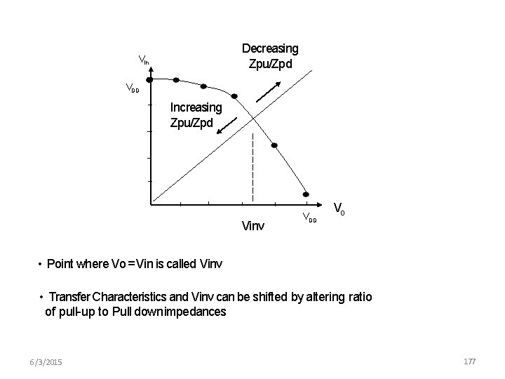
Decreasing Zpu/Zpd Vin VDD Increasing Zpu/Zpd Vinv VDD Vo • Point where Vo = Vin is called Vinv • Transfer Characteristics and Vinv can be shifted by altering ratio of pull-up to Pull down impedances 6/3/2015 177

NMOS Depletion Mode Inverter Characteristics • Dissipation is high since rail to rail current flows when Vin = Logical 1 • Switching of Output from 1 to 0 begins when Vin exceeds Vt of pull down device • When switching the output from 1 to 0, the pull up device is non-saturated initially and this presents a lower resistance through which to charge capacitors (Vds < Vgs – Vt) 6/3/2015 178

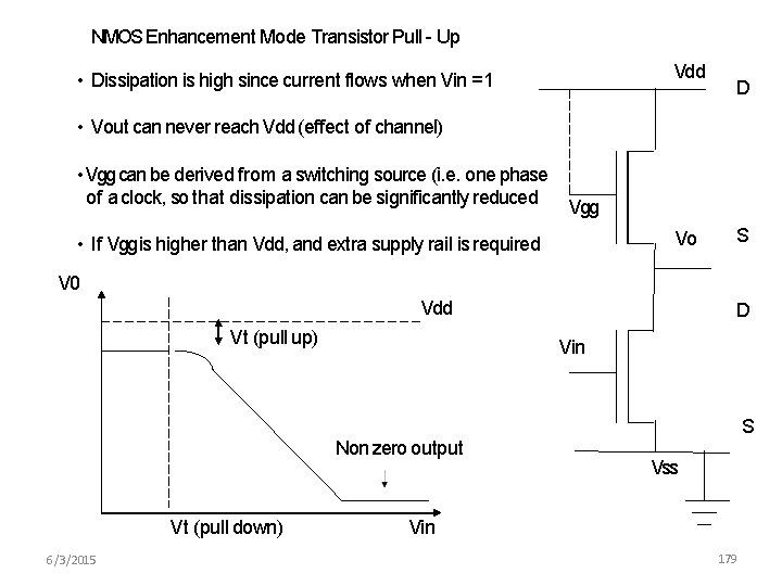
NMOS Enhancement Mode Transistor Pull - Up Vdd • Dissipation is high since current flows when Vin = 1 D • Vout can never reach Vdd (effect of channel) • Vgg can be derived from a switching source (i. e. one phase of a clock, so that dissipation can be significantly reduced Vgg Vo • If Vgg is higher than Vdd, and extra supply rail is required S V 0 Vdd Vt (pull up) Vin Non zero output Vt (pull down) 6/3/2015 D S Vss Vin 179

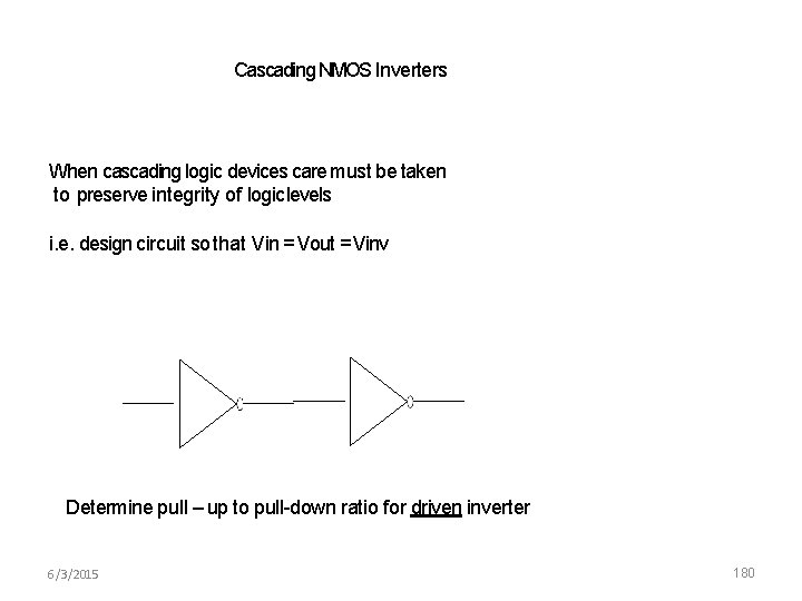
Cascading NMOS Inverters When cascading logic devices care must be taken to preserve integrity of logic levels i. e. design circuit so that Vin = Vout = Vinv Determine pull – up to pull-down ratio for driven inverter 6/3/2015 180

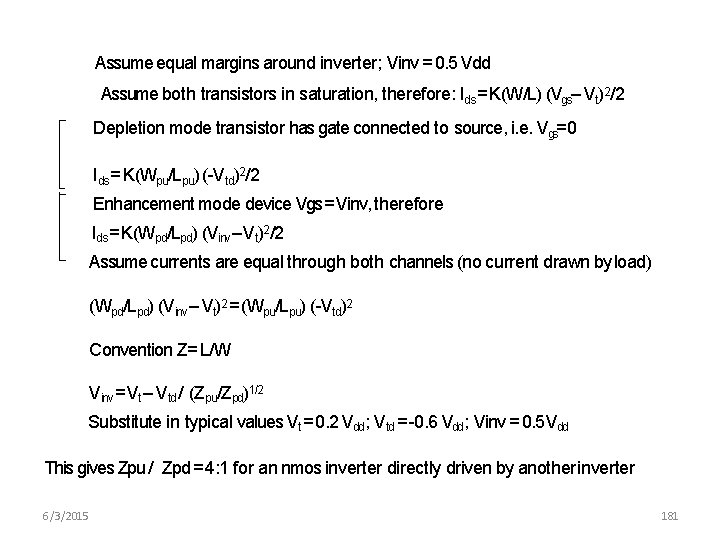
Assume equal margins around inverter; Vinv = 0. 5 Vdd Assume both transistors in saturation, therefore: Ids = K(W/L) (Vgs– Vt)2/2 Depletion mode transistor has gate connected to source, i. e. Vgs=0 Ids = K(Wpu/Lpu) (-Vtd)2/2 Enhancement mode device Vgs = Vinv, therefore Ids = K(Wpd/Lpd) (Vinv –Vt)2/2 Assume currents are equal through both channels (no current drawn by load) (Wpd/Lpd) (Vinv – Vt)2 = (Wpu/Lpu) (-Vtd)2 Convention Z= L/W Vinv = Vt – Vtd / (Zpu/Zpd)1/2 Substitute in typical values Vt = 0. 2 Vdd; Vtd = -0. 6 Vdd; Vinv = 0. 5 Vdd This gives Zpu / Zpd = 4: 1 for an nmos inverter directly driven by another inverter 6/3/2015 181

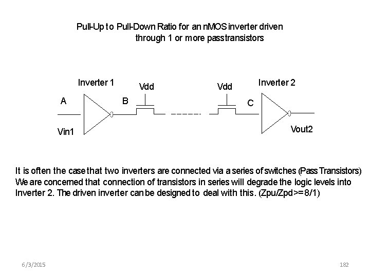
Pull-Up to Pull-Down Ratio for an n. MOS inverter driven through 1 or more pass transistors Inverter 1 A Vin 1 Vdd B Inverter 2 Vdd C Vout 2 It is often the case that two inverters are connected via a series of switches (Pass Transistors) We are concerned that connection of transistors in series will degrade the logic levels into Inverter 2. The driven inverter can be designed to deal with this. (Zpu/Zpd >= 8/1) 6/3/2015 182

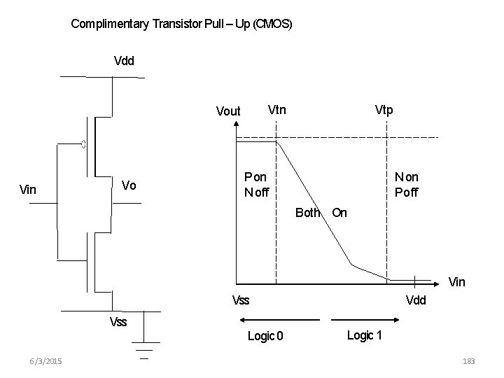
Complimentary Transistor Pull – Up (CMOS) Vdd Vtn Vout Vin Vo Vtp P on N off N on Poff Both On Vin Vdd Vss Logic 0 6/3/2015 Logic 1 183

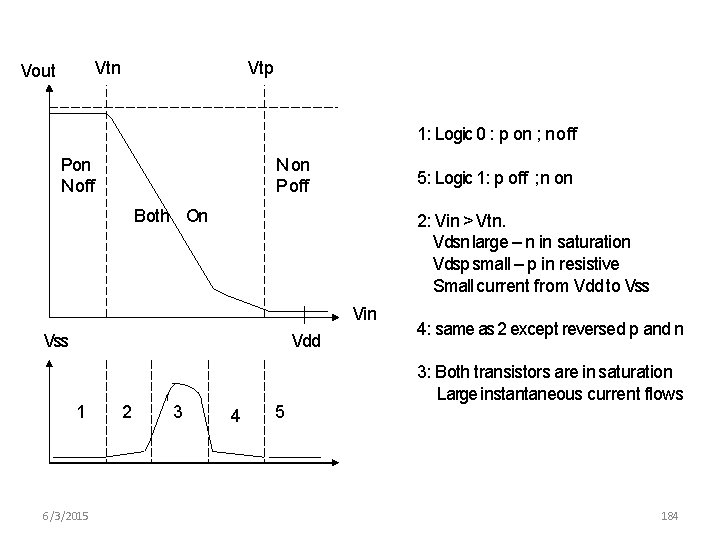
Vtn Vout Vtp 1: Logic 0 : p on ; n off Pon N off N on Poff 5: Logic 1: p off ; n on Both On 2: Vin > Vtn. Vdsn large – n in saturation Vdsp small – p in resistive Small current from Vdd to Vss Vin Vss Vdd 1 6/3/2015 2 3 4 5 4: same as 2 except reversed p and n 3: Both transistors are in saturation Large instantaneous current flows 184

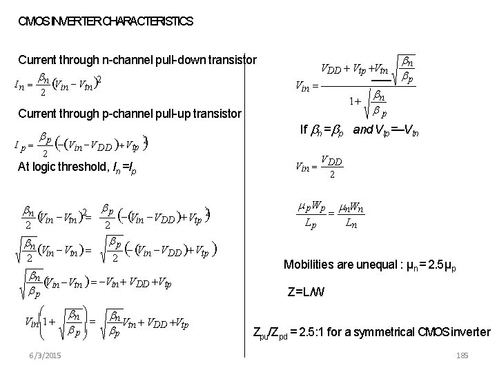
CMOSINVERTERCHARACTERISTICS Current through n-channel pull-down transistor n 2 In 2 Vin Vtn Current through p-channel pull-up transistor I p p 2 Vin VDD Vtp 2 2 n 2 Vin Vtn p 2 Vin VDD Vtp p 2 2 Vin VDD Vtp n Vin Vtn Vin VDD Vtp p Vin 1 6/3/2015 n p n V V V p tn DD tp Vin 1 n p If n = p and Vtp =–Vtn V Vin DD 2 At logic threshold, In =Ip n VDD Vtp Vtn p. W p Lp W n n Ln Mobilities are unequal : µn = 2. 5 µp Z= L/W Zpu/Zpd = 2. 5: 1 for a symmetrical CMOS inverter 185

CMOS Inverter Characteristics • No current flow for either logical 1 or logical 0 inputs • Full logical 1 and 0 levels are presented at the output • For devices of similar dimensions the p – channel is slower than the n – channel device 6/3/2015 186

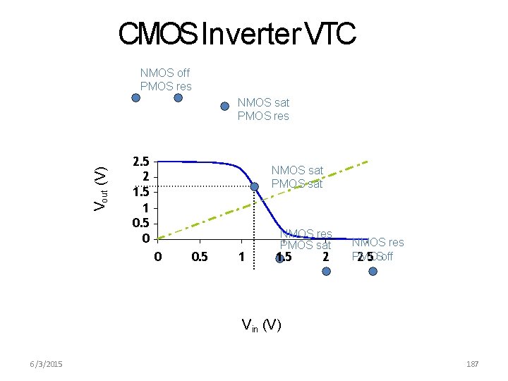
CMOS Inverter VTC NMOS off PMOS res Vout (V) NMOS sat PMOS res 2. 5 2 1. 5 1 0. 5 0 NMOS sat PMOS sat 0 0. 5 1 NMOS res PMOS sat 1. 5 2 NMOS res P 2 M. 5 OSoff Vin (V) 6/3/2015 187

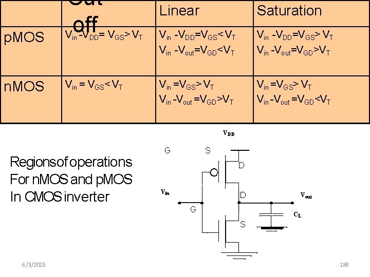
p. MOS Cut off V -V = V n. MOS Vin = VGS< VT in DD GS> VT Linear Saturation Vin -VDD=VGS< VT Vin -Vout=VGD< VT Vin -VDD=VGS> VT Vin -Vout=VGD>VT Vin =VGS> VT Vin -Vout =VGD<VT VDD Regionsof operations For n. MOS and p. MOS In CMOS inverter G S D Vin D G Vout CL S 6/3/2015 188

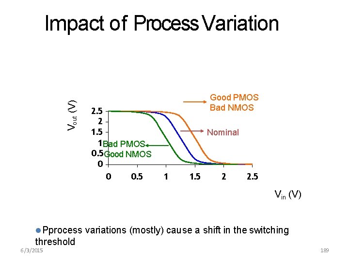
Vout (V) Impact of Process Variation 2. 5 2 1. 5 1 Bad PMOS 0. 5 Good NMOS 0 0 0. 5 Good PMOS Bad NMOS Nominal 1 1. 5 2 2. 5 Vin (V) Pprocess variations (mostly) cause a shift in the switching threshold 6/3/2015 189

Cmos Inverter • Look at why our NMOS and PMOS inverters might not be the best inverter designs • Introduce the CMOS inverter • Analyze how the CMOS inverter works 6/3/2015 190

NMOS Inverter 5 V 5 V When s V to is logic 1, V 0, itsransistor gets • When VIN change logic 0. cutoff. ID goes. Constant to 0. nonzero current R R sh rt ousghto arz t nsesrioo t. . r • ‘esistor voltagelf owgo e VOUT “pulled Power is used even though D V I = 5 / R up ” t o 5 V. no new computation is being D V I =0 IN VIN OUT D + 5 V 6/3/2015 OUT VDS _ 0 V performed. VIN D + 0 V OUT 5 V VDS _ 191

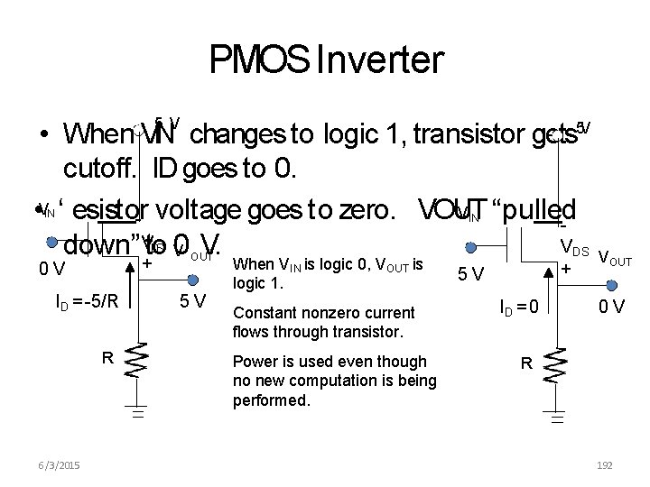
PMOS Inverter 5 V • When VIN changes to logic 1, transistor gets 5 V cutoff. ID goes to 0. V T “pulled • V ‘ esisto-r voltage goes to zero. VOU V down”Vto 0 V V. V IN IN DS + 0 V ID = -5/R R 6/3/2015 OUT 5 V When VIN is logic 0, VOUT is logic 1. Constant nonzero current flows through transistor. Power is used even though no new computation is being performed. DS + 5 V ID = 0 OUT 0 V R 192

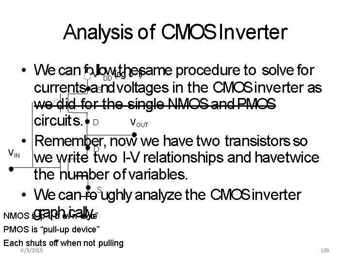
Analysis of CMOS Inverter • We can fo. Vlow(Lotghcie 1 same procedure to solve for ) currents a. Snd voltages in the CMOS inverter as we did for the single NMOS and PMOS V circuits. D • Remember, now we have two transistors so D V we write two I-V relationships and havetwice the number of variables. S • We can ro ughly analyze the CMOSinverter i nadelvlyci. e” NMOS sig“rpaup l -ldhowc DD OUT IN PMOS is “pull-up device” Each shuts off when not pulling 6/3/2015 193

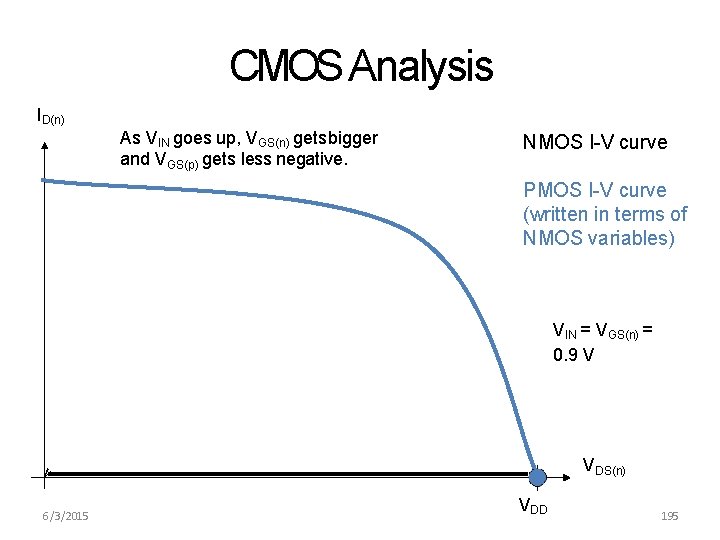
CMOS Analysis ID(n) As VIN goes up, VGS(n) gets bigger and VGS(p) gets less negative. NMOS I-V curve PMOS I-V curve (written in terms of NMOS variables) VIN = VGS(n) = 0. 9 V VDS(n) 6/3/2015 VDD 195

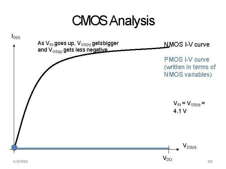
CMOS Analysis ID(n) As VIN goes up, VGS(n) gets bigger and VGS(p) gets less negative. NMOS I-V curve PMOS I-V curve (written in terms of NMOS variables) VIN = VGS(n) = 4. 1 V VDS(n) 6/3/2015 VDD 201

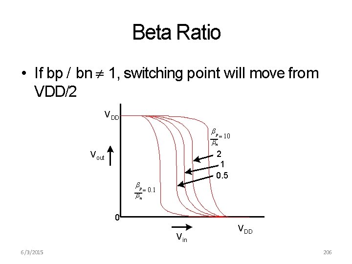
Beta Ratio • If bp / bn 1, switching point will move from VDD/2 VDD p 10 n 2 1 0. 5 Vout p 0. 1 n 0 Vin 6/3/2015 VDD 206

VLSI CIRCUIT DESIGN PROCESSES Topics • VLSI design flow • MOS layers • Stick diagrams • Design Rules and Layout • 2 um CMOS design rules for wires • Contacts and Transistors • Layout diagrams for NMOS and • CMOSinverters and gates, Scaling of MOScircuits 6/3/2015 207

VLSI Design of approach of IC 6 2/038/ 2015

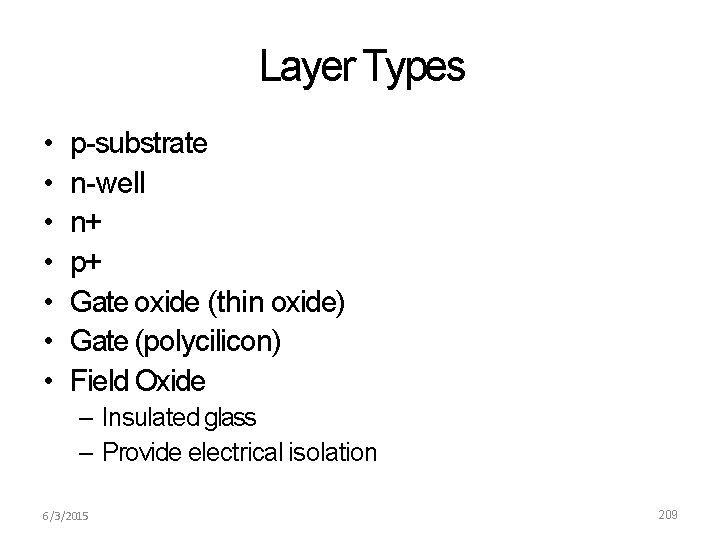
Layer Types • • p-substrate n-well n+ p+ Gate oxide (thin oxide) Gate (polycilicon) Field Oxide – Insulated glass – Provide electrical isolation 6/3/2015 209

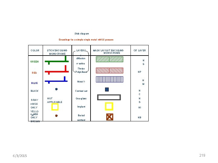
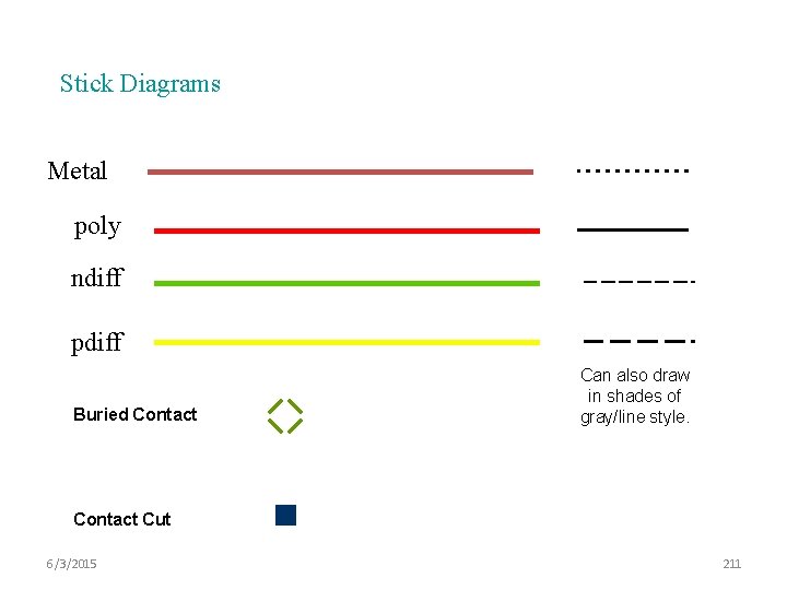
Stick diagram Encodings for a simple single metal n. MOS process COLOR STICK ENCODING MONOCROME GREEN Thniox Polysilicon BLACK YELLO n. WMOS ONLY BROWN 6/3/2015 CIF LAYER N D NP N M Metal 1 BLUE n. MOS ONLY ndiffusion MASK LAYOUT ENCODING MONOCROME n+active RED GRAY LAYERS NOT APPLICABLE Contact cut N C Overglass N G Implant NI Buried contact NB 219

Stick Diagrams Metal poly ndiff pdiff Buried Contact Can also draw in shades of gray/line style. Contact Cut 6/3/2015 211

Stick Diagrams • VLSI design aims to translate circuit concepts onto silicon. • Stick diagrams are a means of capturing topography and layer information using simple diagrams. • Stick diagrams convey layer information through colour codes (or monochrome encoding). • Acts as an interface between symbolic circuit and the actual layout. 6/3/2015 212

Stick Diagrams • Does show all components/vias. • It shows relative placement of components. • Goes one step closer to the layout • Helps plan the layout and routing 6/3/2015 213

Stick Diagrams • Does not show – Exact placement of components – Transistor sizes – Wire lengths, wire widths, tub boundaries. – Any other low level details such as parasitics. . 6/3/2015 214

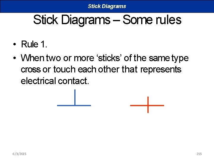
Stick Diagrams – Some rules • Rule 1. • When two or more ‘sticks’ of the same type cross or touch each other that represents electrical contact. 6/3/2015 215

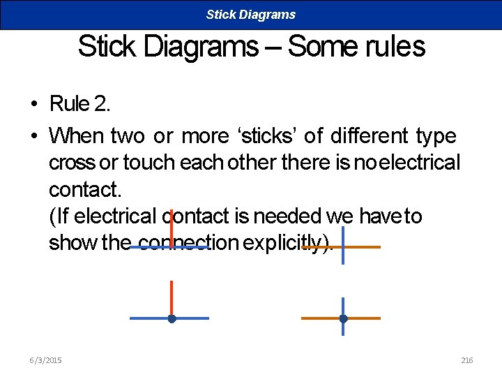
Stick Diagrams – Some rules • Rule 2. • When two or more ‘sticks’ of different type cross or touch each othere is noelectrical contact. (If electrical contact is needed we have to show the connection explicitly). 6/3/2015 216

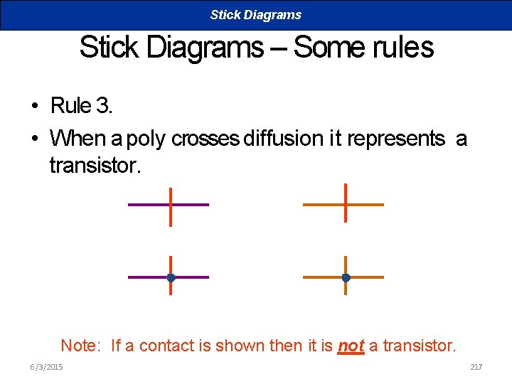
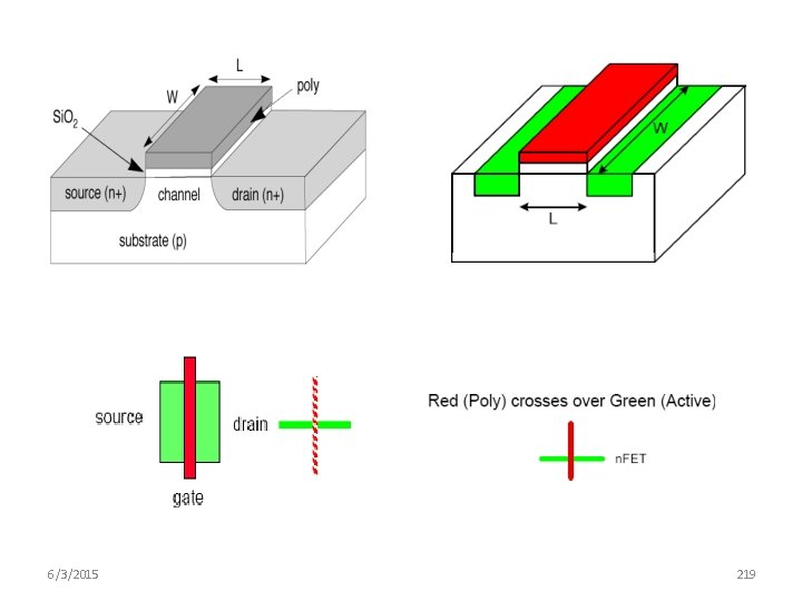
Stick Diagrams – Some rules • Rule 3. • When a poly crosses diffusion it represents a transistor. Note: If a contact is shown then it is not a transistor. 6/3/2015 217

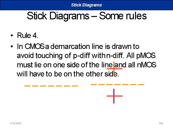
Stick Diagrams – Some rules • Rule 4. • In CMOS a demarcation line is drawn to avoid touching of p-diff with n-diff. All p. MOS must lie on one side of the line and all n. MOS will have to be on the other side. 6/3/2015 218

6/3/2015 219

NMOS INVERTER 5 V 5 v Dep Vout Enh Vin 0 V 0 V 6/3/2015 220

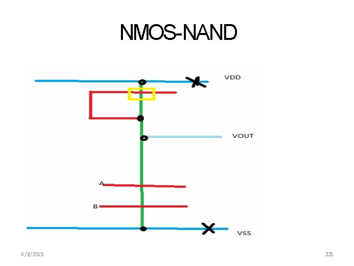
NMOS-NAND 6/3/2015 221

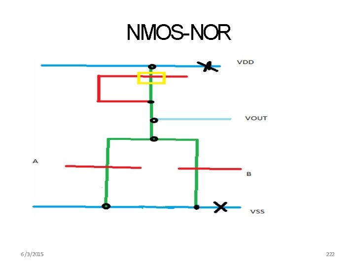
NMOS-NOR 6/3/2015 222

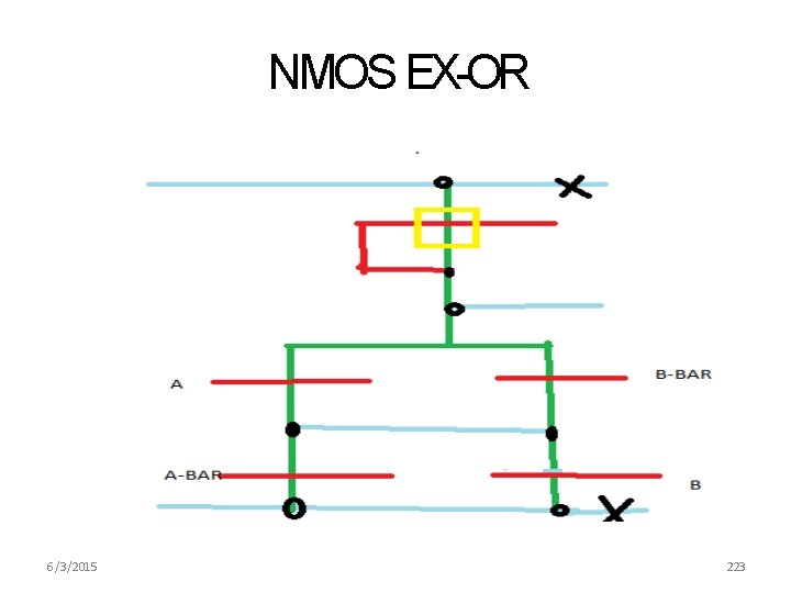
NMOS EX-OR 6/3/2015 223

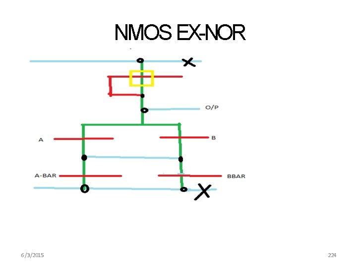
NMOS EX-NOR 6/3/2015 224

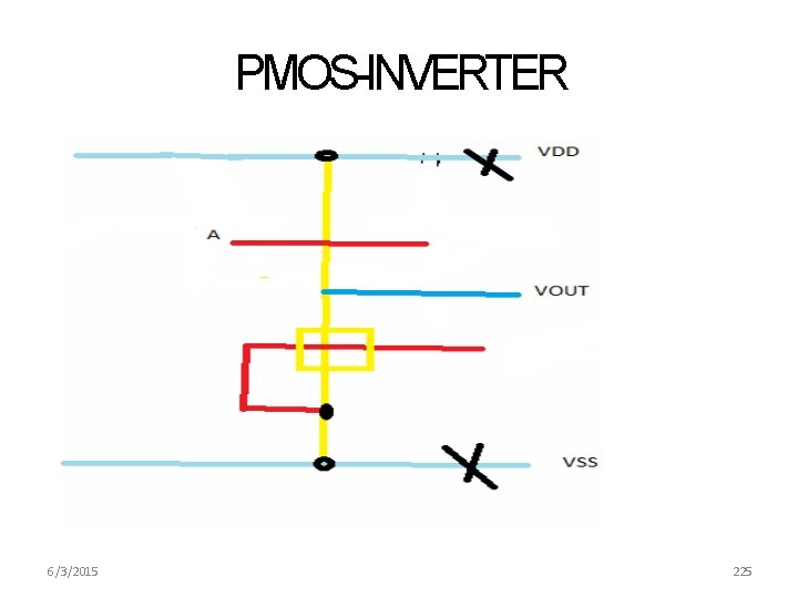
PMOS-INVERTER 6/3/2015 225

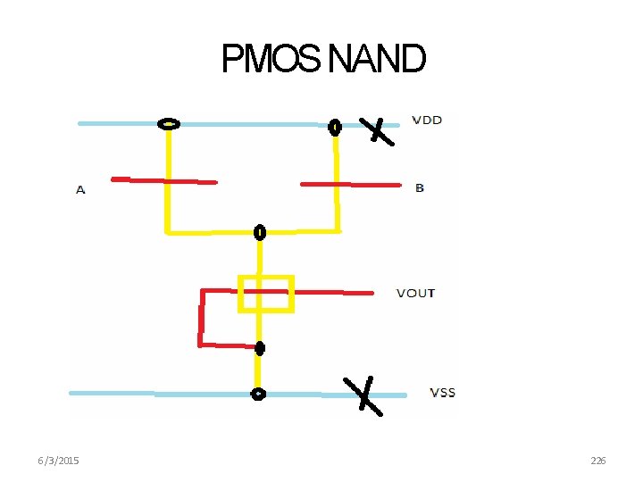
PMOS NAND 6/3/2015 226

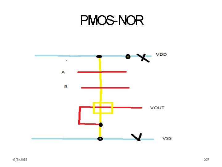
PMOS-NOR 6/3/2015 227

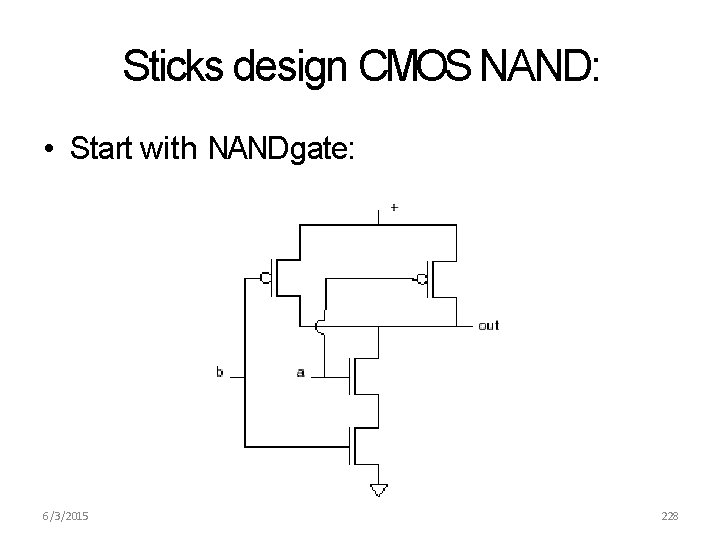
Sticks design CMOS NAND: • Start with NAND gate: 6/3/2015 228

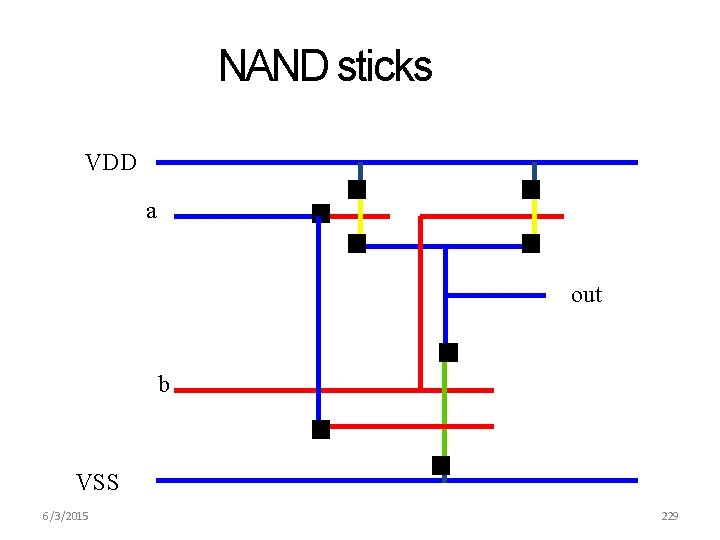
NAND sticks VDD a out b VSS 6/3/2015 229

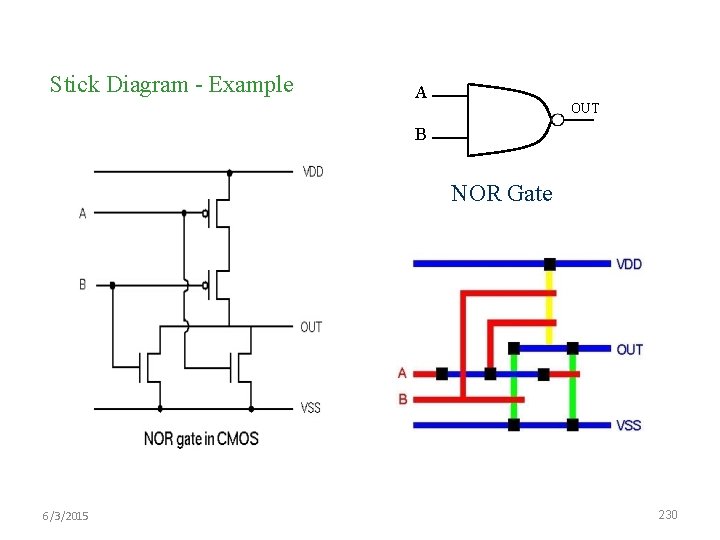
Stick Diagram - Example A OUT B NOR Gate 6/3/2015 230

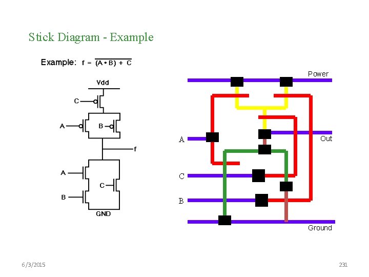
Stick Diagram - Example Power A Out C B Ground 6/3/2015 231

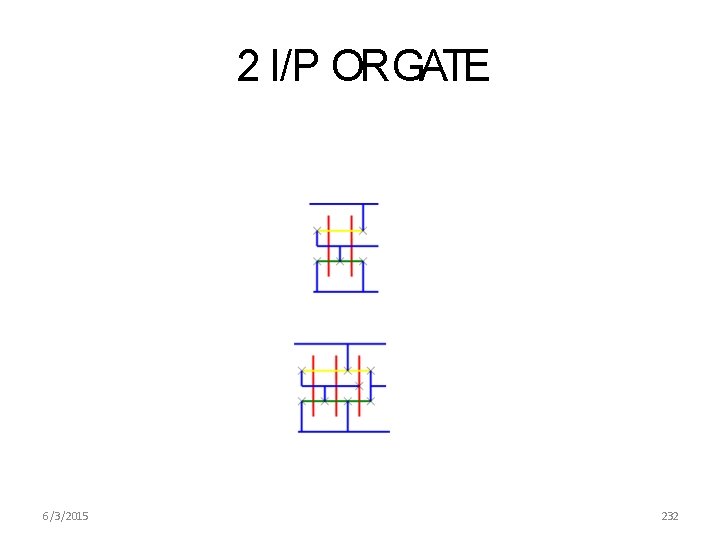
2 I/P ORGATE 6/3/2015 232

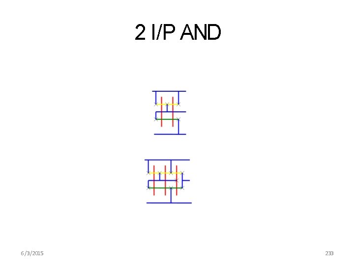
2 I/P AND 6/3/2015 233

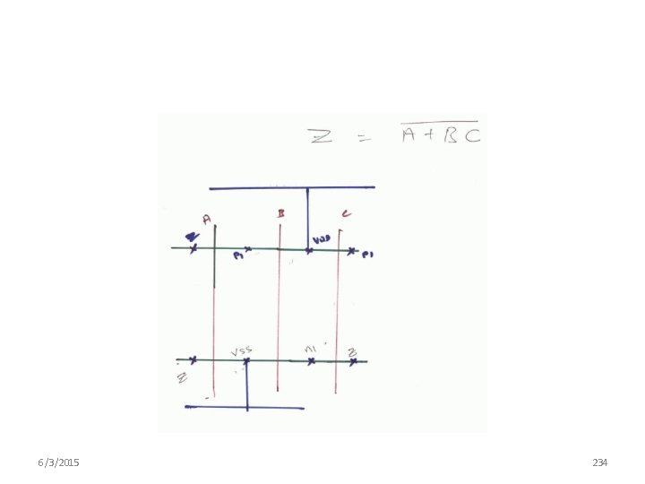
6/3/2015 234

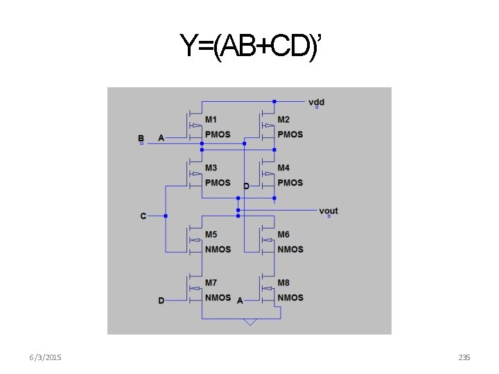
Y=(AB+CD)’ 6/3/2015 235

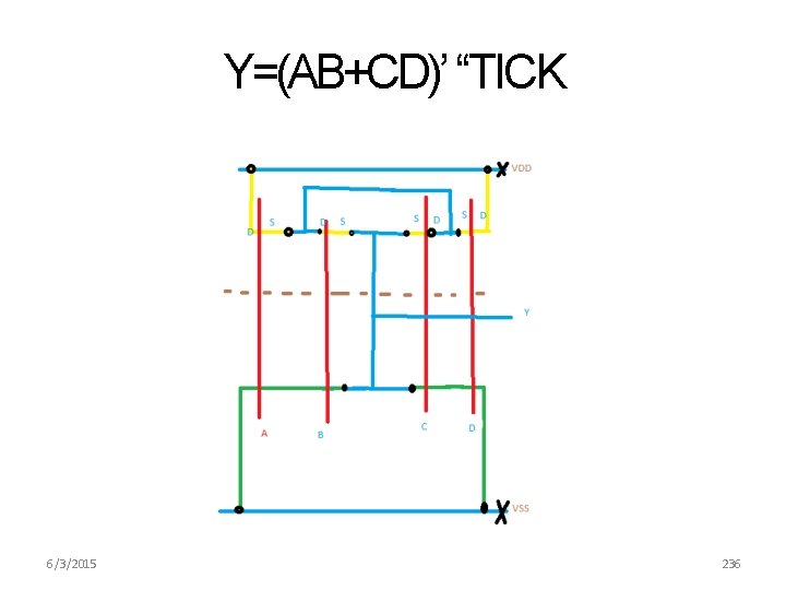
Y=(AB+CD)’ “TICK 6/3/2015 236

6/3/2015 237

Design Rules • Design rules are a set of geometrical specifications that dictate the design of the layout masks • A design rule set provides numerical values – For minimum dimensions – For minimum line spacings • Design rules must be followed to insure functional structures on the fabricated chip • Design rules change with technological advances (www. mosis. org) 6/3/2015 238

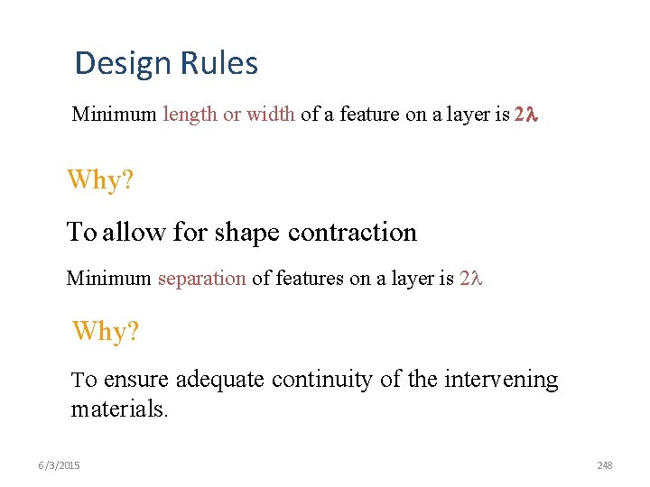
Design Rules Minimum length or width of a feature on a layer is 2 Why? To allow for shape contraction Minimum separation of features on a layer is 2 Why? To ensure adequate continuity of the intervening materials. 6/3/2015 248

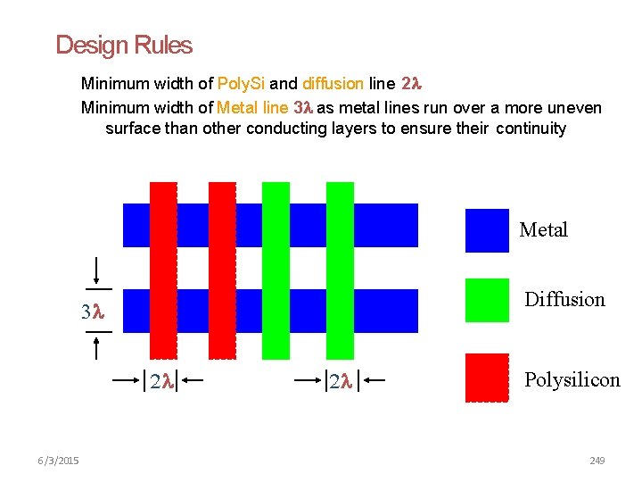
Design Rules Minimum width of Poly. Si and diffusion line 2 Minimum width of Metal line 3 as metal lines run over a more uneven surface than other conducting layers to ensure their continuity Metal Diffusion 6/3/2015 Polysilicon 249

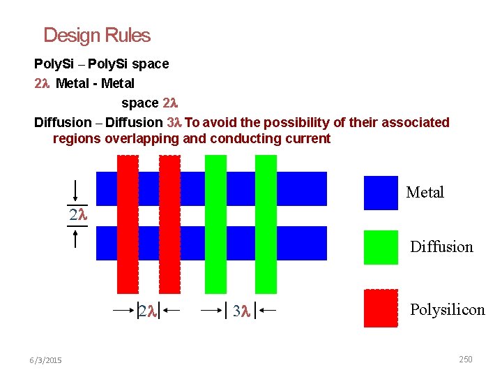
Design Rules Poly. Si – Poly. Si space 2 Metal - Metal space 2 Diffusion – Diffusion 3 To avoid the possibility of their associated regions overlapping and conducting current Metal Diffusion 6/3/2015 Polysilicon 250

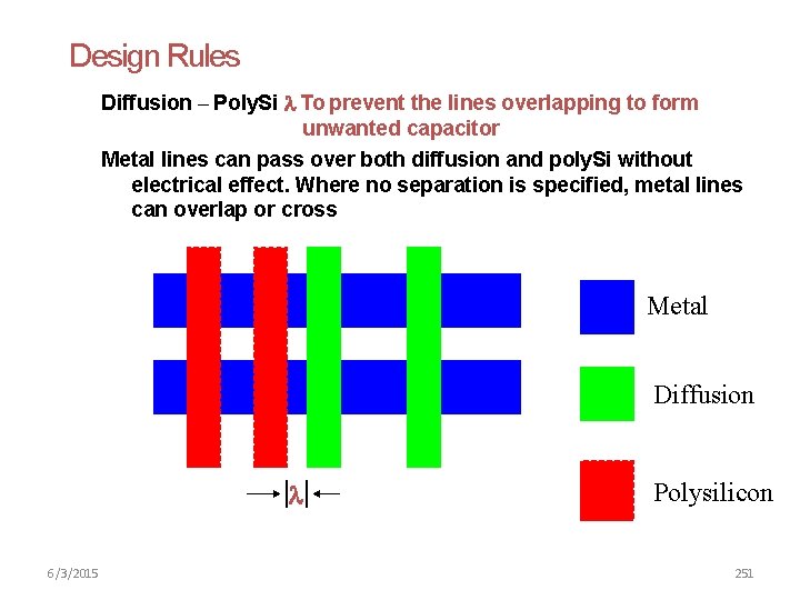
Design Rules Diffusion – Poly. Si To prevent the lines overlapping to form unwanted capacitor Metal lines can pass over both diffusion and poly. Si without electrical effect. Where no separation is specified, metal lines can overlap or cross Metal Diffusion 6/3/2015 Polysilicon 251

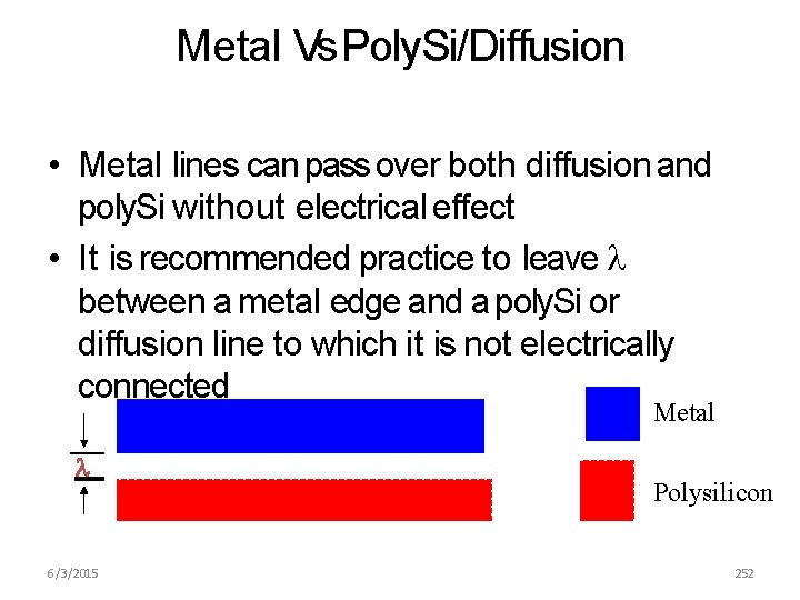
Metal Vs Poly. Si/Diffusion • Metal lines can pass over both diffusion and poly. Si without electrical effect • It is recommended practice to leave between a metal edge and a poly. Si or diffusion line to which it is not electrically connected Metal 6/3/2015 Polysilicon 252

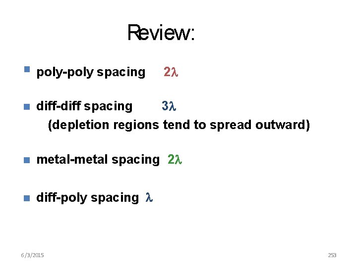
Review: poly-poly spacing 2 diff-diff spacing 3 (depletion regions tend to spread outward) metal-metal spacing 2 diff-poly spacing 6/3/2015 253

Note • Two Features on different mask layers can be misaligned by a maximum of 2 l on the wafer. • If the overlap of these two different mask layers can be catastrophic to the design, they must be separated by at least 2 l • If the overlap is just undesirable, they must be separated by at least l 6/3/2015 254

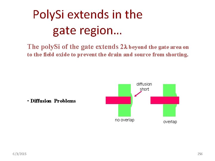
When a transistor is formed? Gate is formed where poly. Si crosses diffusion with thin oxide between these layers. Design rules min. line width of poly. Si and diffusion 2 drain and source have min. length and width of 2 And 6/3/2015 255

Poly. Si extends in the gate region… The poly. Si of the gate extends 2 beyond the gate area on to the field oxide to prevent the drain and source from shorting. diffusion short • Diffusion Problems no overlap 6/3/2015 overlap 256

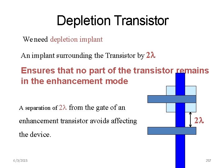
Depletion Transistor We need depletion implant An implant surrounding the Transistor by 2 Ensures that no part of the transistor remains in the enhancement mode A separation of 2 from the gate of an enhancement transistor avoids affecting 2 the device. 6/3/2015 257

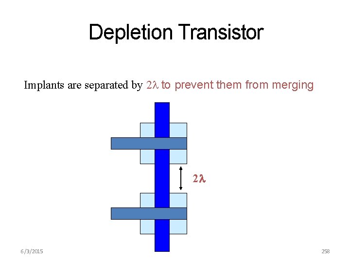
Depletion Transistor Implants are separated by 2 to prevent them from merging 2 6/3/2015 258

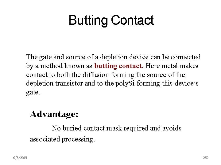
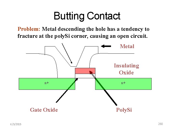
Butting Contact The gate and source of a depletion device can be connected by a method known as butting contact. Here metal makes contact to both the diffusion forming the source of the depletion transistor and to the poly. Si forming this device’s gate. Advantage: No buried contact mask required and avoids associated processing. 6/3/2015 259

Butting Contact Problem: Metal descending the hole has a tendency to fracture at the poly. Si corner, causing an open circuit. Metal Insulating Oxide n+ Gate Oxide 6/3/2015 n+ Poly. Si 260

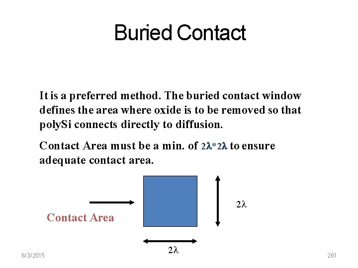
Buried Contact It is a preferred method. The buried contact window defines the area where oxide is to be removed so that poly. Si connects directly to diffusion. Contact Area must be a min. of 2 *2 to ensure adequate contact area. 2 Contact Area 6/3/2015 2 261

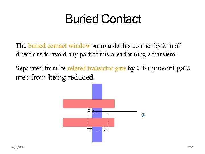
Buried Contact The buried contact window surrounds this contact by in all directions to avoid any part of this area forming a transistor. Separated from its related transistor gate by to prevent gate area from being reduced. 6/3/2015 262

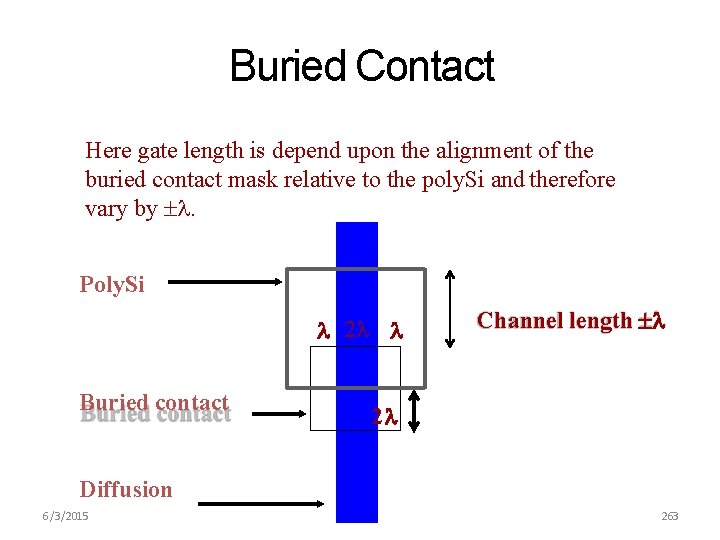
Buried Contact Here gate length is depend upon the alignment of the buried contact mask relative to the poly. Si and therefore vary by . Poly. Si 2 Buried contact Channel length 2 Diffusion 6/3/2015 263

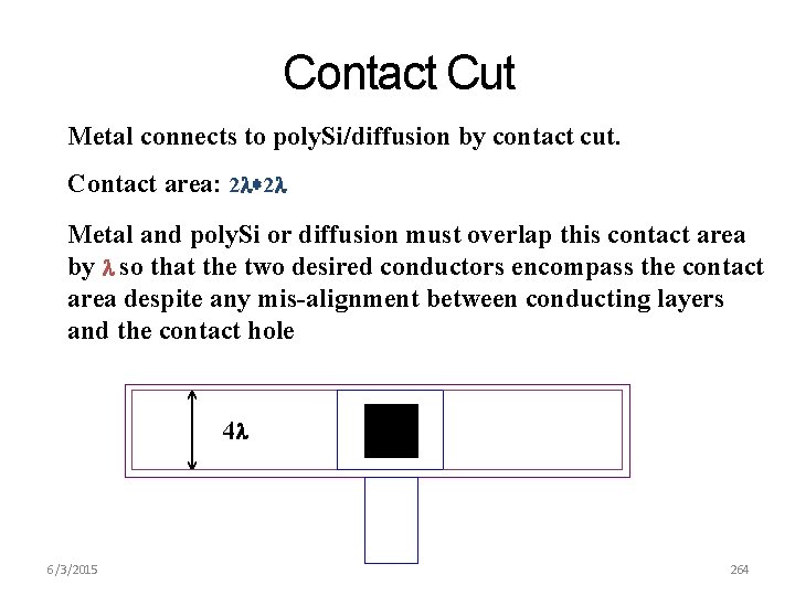
Contact Cut Metal connects to poly. Si/diffusion by contact cut. Contact area: 2 2 Metal and poly. Si or diffusion must overlap this contact area by so that the two desired conductors encompass the contact area despite any mis-alignment between conducting layers and the contact hole 4 6/3/2015 264

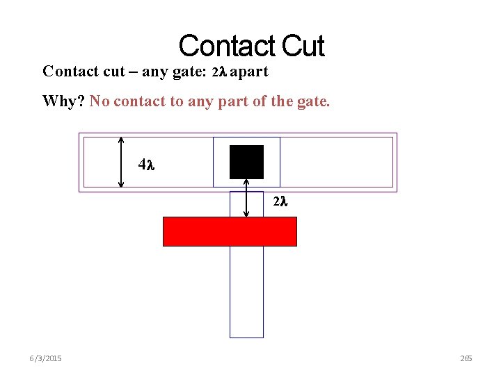
Contact Cut Contact cut – any gate: 2 apart Why? No contact to any part of the gate. 4 2 6/3/2015 265

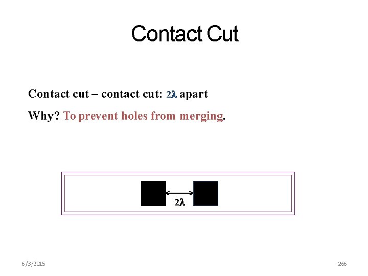
Contact Cut Contact cut – contact cut: 2 apart Why? To prevent holes from merging. 2 6/3/2015 266

Rules for CMOS layout Similar to those for NMOS except No 1. Depletion implant 2. Buried contact Additional rules 1. Definition of n-well area 2. Threshold implant of two types of transistor 3. Definition of source and drains regions for the NMOS and PMOS. 6/3/2015 267

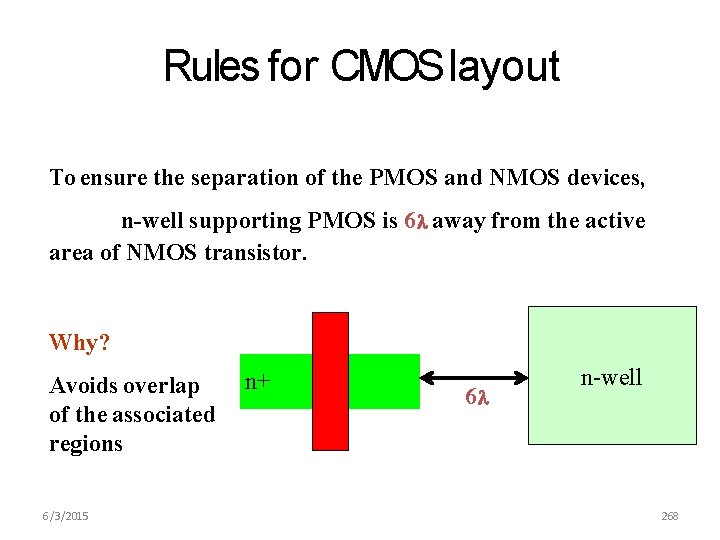
Rules for CMOS layout To ensure the separation of the PMOS and NMOS devices, n-well supporting PMOS is 6 away from the active area of NMOS transistor. Why? Avoids overlap of the associated regions 6/3/2015 n+ 6 n-well 268

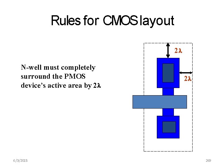
Rules for CMOS layout 2 N-well must completely surround the PMOS device’s active area by 2 6/3/2015 2 269

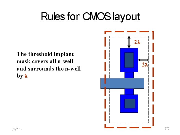
Rules for CMOS layout 2 The threshold implant mask covers all n-well and surrounds the n-well by 6/3/2015 2 270

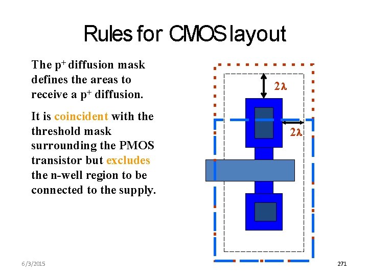
Rules for CMOS layout The p+ diffusion mask defines the areas to receive a p+ diffusion. It is coincident with the threshold mask surrounding the PMOS transistor but excludes the n-well region to be connected to the supply. 6/3/2015 2 2 271

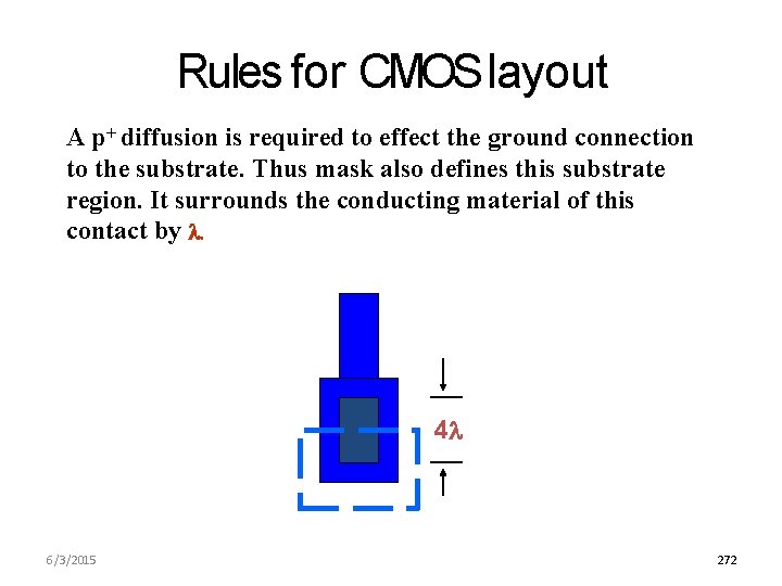
Rules for CMOS layout A p+ diffusion is required to effect the ground connection to the substrate. Thus mask also defines this substrate region. It surrounds the conducting material of this contact by 4 6/3/2015 272

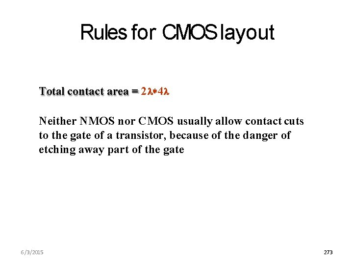
Rules for CMOS layout Total contact area = 2 4 Neither NMOS nor CMOS usually allow contact cuts to the gate of a transistor, because of the danger of etching away part of the gate 6/3/2015 273