Process integration 1 cleaning sheet resistance and resistors
- Slides: 25

Process integration 1: cleaning, sheet resistance and resistors, thermal budget, front end sami. franssila@aalto. fi

Wafer selection • active role for the wafer ? • passive role ? – thermal conductivity – optical transparency – flat, smooth mechanical support • compatibility with equipment ? • thermal limitations ? • contamination ? Especially glass in Si fabs !

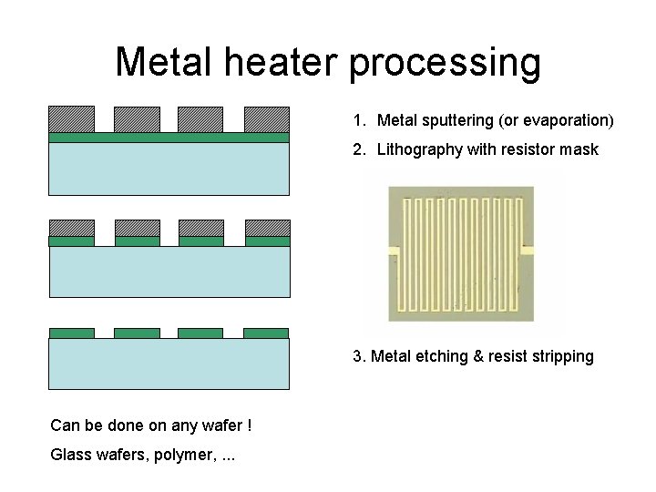
Metal heater processing 1. Metal sputtering (or evaporation) 2. Lithography with resistor mask 3. Metal etching & resist stripping Can be done on any wafer ! Glass wafers, polymer, . . .

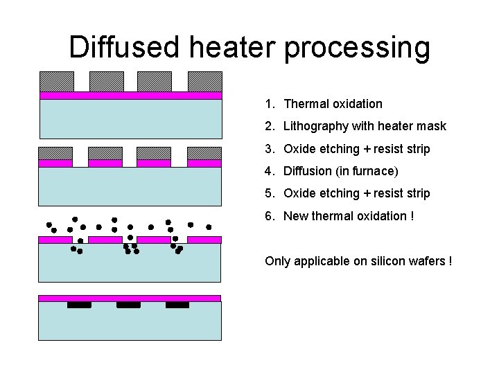
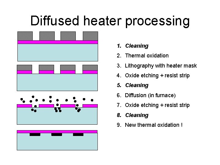
Diffused heater processing 1. Thermal oxidation 2. Lithography with heater mask 3. Oxide etching + resist strip 4. Diffusion (in furnace) 5. Oxide etching + resist strip 6. New thermal oxidation ! Only applicable on silicon wafers !

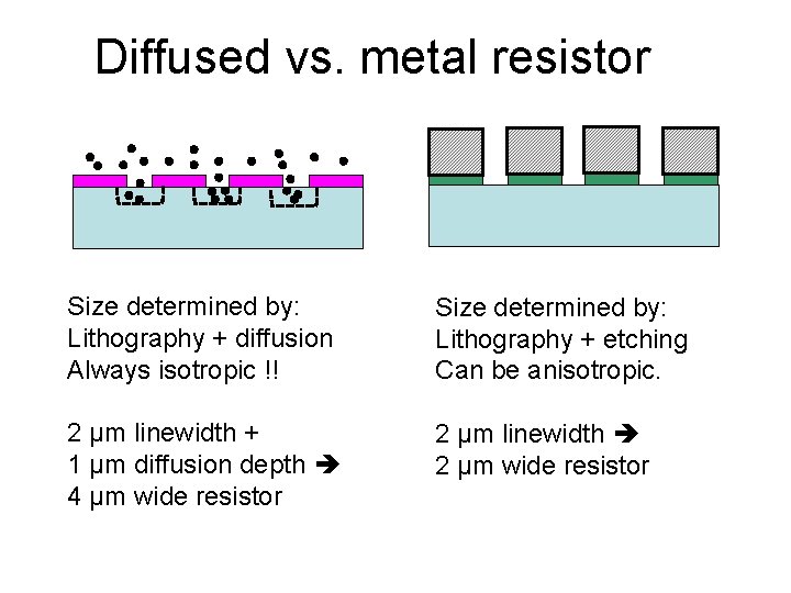
Diffused vs. metal resistor Size determined by: Lithography + diffusion Always isotropic !! Size determined by: Lithography + etching Can be anisotropic. 2 µm linewidth + 1 µm diffusion depth 4 µm wide resistor 2 µm linewidth 2 µm wide resistor

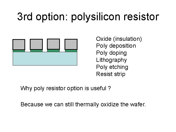
3 rd option: polysilicon resistor Oxide (insulation) Poly deposition Poly doping Lithography Poly etching Resist strip Why poly resistor option is useful ? Because we can still thermally oxidize the wafer.

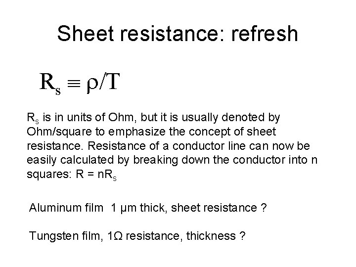
Sheet resistance: refresh Rs /T Rs is in units of Ohm, but it is usually denoted by Ohm/square to emphasize the concept of sheet resistance. Resistance of a conductor line can now be easily calculated by breaking down the conductor into n squares: R = n. Rs Aluminum film 1 µm thick, sheet resistance ? Tungsten film, 1Ω resistance, thickness ?

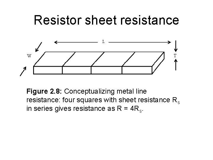
Resistor sheet resistance Figure 2. 8: Conceptualizing metal line resistance: four squares with sheet resistance Rs in series gives resistance as R = 4 Rs.

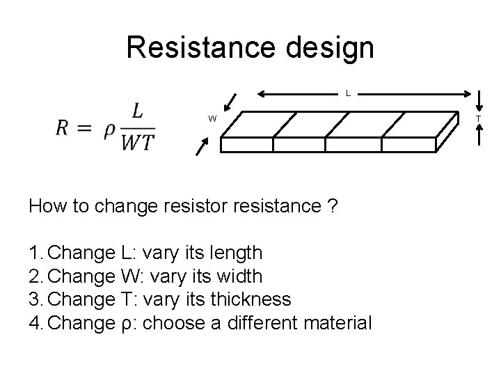
Resistance design L W How to change resistor resistance ? 1. Change L: vary its length 2. Change W: vary its width 3. Change T: vary its thickness 4. Change ρ: choose a different material T

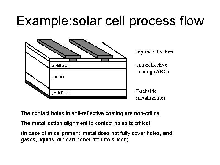
Example: solar cell process flow top metallization n -diffusion anti-reflective coating (ARC) p-substrate p+ diffusion Backside metallization The contact holes in anti-reflective coating are non-critical The metallization alignment to contact holes is critical (in case of misalignment, metal does not fully cover holes, and gases, liquids, dirt can penetrate into silicon)

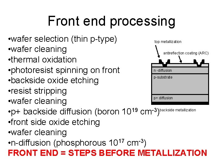
Front end processing • wafer selection (thin p-type) top metallization • wafer cleaning antireflection coating (ARC) • thermal oxidation n -diffusion • photoresist spinning on front p-substrate • backside oxide etching • resist stripping p+ diffusion • wafer cleaning • p+ backside diffusion (boron 1019 cm-3)backside metallization • front side oxide etching • wafer cleaning • n-diffusion (phosphorous 1017 cm-3) FRONT END = STEPS BEFORE METALLIZATION

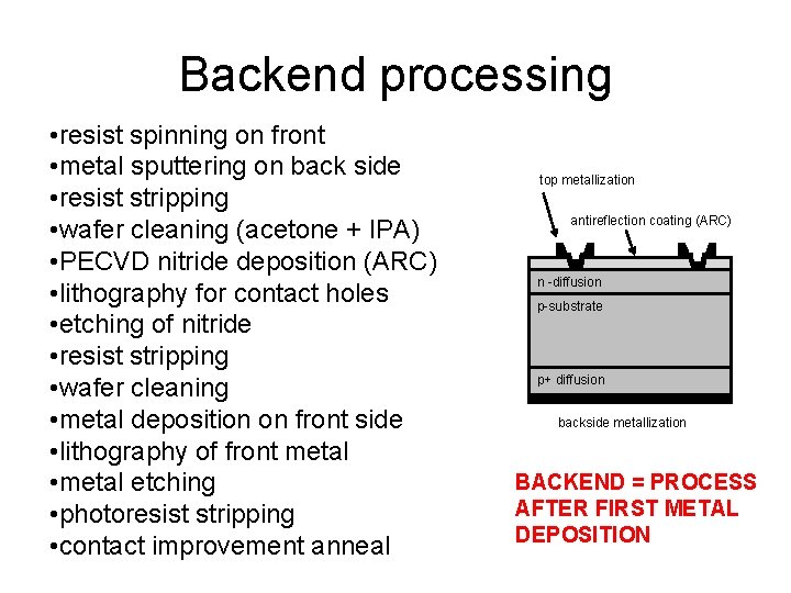
Backend processing • resist spinning on front • metal sputtering on back side • resist stripping • wafer cleaning (acetone + IPA) • PECVD nitride deposition (ARC) • lithography for contact holes • etching of nitride • resist stripping • wafer cleaning • metal deposition on front side • lithography of front metal • metal etching • photoresist stripping • contact improvement anneal top metallization antireflection coating (ARC) n -diffusion p-substrate p+ diffusion backside metallization BACKEND = PROCESS AFTER FIRST METAL DEPOSITION

Active vs. passive cleaning • Cleanroom (and its subsystems) provide passive cleanliness • Wafer cleaning provides active cleaning

Cleaning and surface treatments • Because atoms spread fast at higher temperatures, it is essential to remove impurity atoms before subjecting the wafers to high temperatures. • Wet cleaning: • RCA-1 (NH 4 OH-H 2 O 2): removes particles and organic materials • RCA-2 (HCl-H 2 O 2): removes metallic impurities • HF: removes native oxide (Si. O 2) • Rinsing and drying are integral parts of wet cleaning !! TKK MICRONOVA, 2010 Microfabrication 14

Cleaning & surface treatments (2) -etch surface to undercut particles (unfortunately rougheness increases) -etch film to recover perfect surface (e. g. after oxidation) -grow film to passivate surface (e. g. Al 2 O 3 very sturdy) -after cleaning, wafers are in known state. -memory of previous process steps is eliminated. -waiting time effects are eliminated.

Wafer cleaning • • removal of added contamination ultrapure chemicals (very expensive) particle-free (filtered 0. 3 µm) always includes rinsing & drying steps (with ultrapure water and nitrogen)

Surface preparation • leaves wafer in known surface condition • eliminates previous step peculiarities • eliminates waiting time effects • Wafer cleaning is the same as surface preparation; it is just a different viewpoint of wafer cleanliness

Diffused heater processing 1. Cleaning 2. Thermal oxidation 3. Lithography with heater mask 4. Oxide etching + resist strip 5. Cleaning 6. Diffusion (in furnace) 7. Oxide etching + resist strip 8. Cleaning 9. New thermal oxidation !

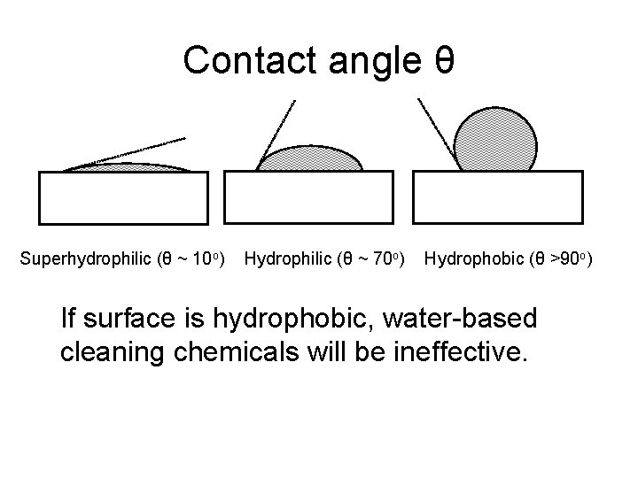
Contact angle θ Superhydrophilic (θ ~ 10 o) Hydrophilic (θ ~ 70 o) Hydrophobic (θ >90 o) If surface is hydrophobic, water-based cleaning chemicals will be ineffective.

Cleaning in practise RCA-1 RCA-2 HF-dip

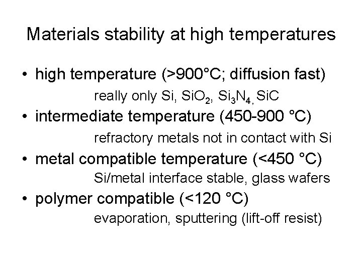
Materials stability at high temperatures • high temperature (>900°C; diffusion fast) really only Si, Si. O 2, Si 3 N 4, Si. C • intermediate temperature (450 -900 °C) refractory metals not in contact with Si • metal compatible temperature (<450 °C) Si/metal interface stable, glass wafers • polymer compatible (<120 °C) evaporation, sputtering (lift-off resist)

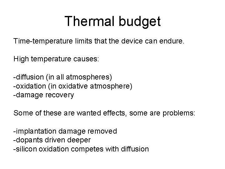
Thermal budget Time-temperature limits that the device can endure. High temperature causes: -diffusion (in all atmospheres) -oxidation (in oxidative atmosphere) -damage recovery Some of these are wanted effects, some are problems: -implantation damage removed -dopants driven deeper -silicon oxidation competes with diffusion

Thermal budget 2 Concrete examples of junction depths,

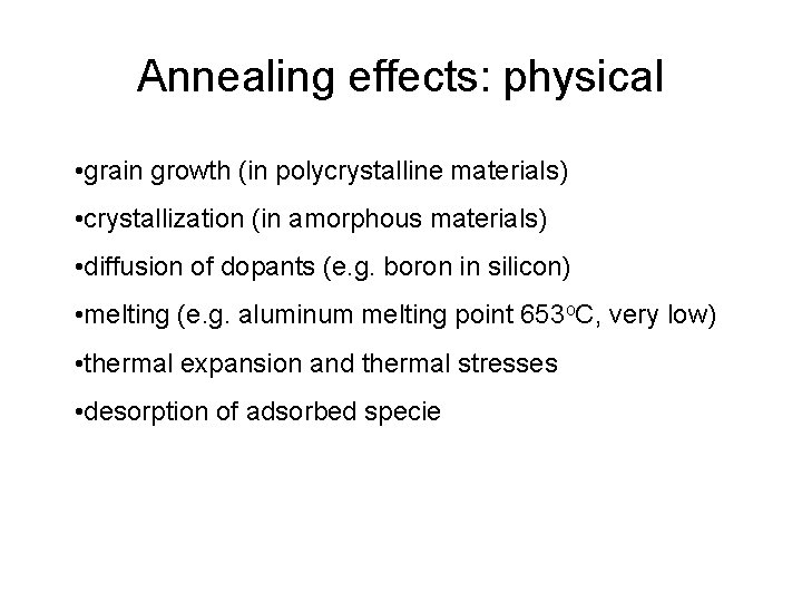
Annealing effects: physical • grain growth (in polycrystalline materials) • crystallization (in amorphous materials) • diffusion of dopants (e. g. boron in silicon) • melting (e. g. aluminum melting point 653 o. C, very low) • thermal expansion and thermal stresses • desorption of adsorbed specie

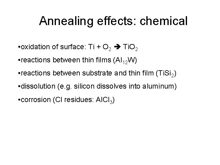
Annealing effects: chemical • oxidation of surface: Ti + O 2 Ti. O 2 • reactions between thin films (Al 12 W) • reactions between substrate and thin film (Ti. Si 2) • dissolution (e. g. silicon dissolves into aluminum) • corrosion (Cl residues: Al. Cl 3)