Rangkaian Logika Sekuensial Sinkron Synchronous Sequential Logic Chapter
")


")


 LATCH Versi NOR Gate (SR Latch)")
 LATCH Versi NAND Gate (S'R' Latch) Q=1")


 v. D=HIGH a SET state")


 • State = Nilai")
 = DA = A(t)")
 Present Input State A 0")
 • Penulisan lain Present")
 Present Input State A")


 Q(t+1) 0 0 0 1 1 F.")


 =")


- Slides: 59
Rangkaian Logika Sekuensial Sinkron Synchronous Sequential Logic (Chapter 5 – Mano)
Combinational v. s Sequential Logic Combinational Logic: Sequential Logic: • Output hanya tergantung dari kombinasi input saat itu • Dapat digunakan untuk berbgai operasi (add/subtract/multiply/en code/decode/select[mux] /etc…) • Perlu mengkombinasikan berbagai strukutur secara tersusun • Tidak fleksibel dan lebih mahal • Output tergantung dari input saat itu dan juga output sebelumnya • Dapat menyimpan informasi antar operasiopearasi • Memerlukan beberapa jenis memory (disebut sbg Register) untuk mengingat nilai output sebelumnya. (Biasanya menggunakan D Flip Flop sebagai Registers)
Logika Sekuensial
Logika Sekuensial • Sequential Logic circuits remember past • inputs and past circuit state. • Outputs from the system are“fed back” as new inputs. • The memory elements are circuits that are capable of storing binary information
Sinkron v. s Asinkron There are two types of sequential circuits: • Synchronous sequential circuit: Output berubah pada waktu-waktu tertentu. Penentuan waktu menggunakan sinyal timing yang disebut sebagai clock. • Asynchronous (fundamental mode) sequential circuit: Output berubah setiap saat tergantung pada urutan perubahan sinyal input. Rangkain ini tidak memerlukan clock (clockless).
Logika Sekuensial Sinkron
Pulsa Clock Positive pulses Positive edges Negative edges
Latches dan Flip-Flop § Multivibrator: jenis rangkaian sekuensial. Ada 3 jenis: vbistable (2 kondisi) vmonostable or one-shot (1 kondisi stabil) vastable (tidak ada kondisi stabil, selalu berubah) § Bistable logic devices: latches dan flip-flops. § Latches dan flip-flop berbeda dalama hal bagaimana cara perubahan state-nya
Memory Elements § Memory element: Sebuah perangkat yang dapat mengingat nilai sebelumnya atau mengubah nilai berdasarkan perintah(command) dari inputnya. command Memory element Q stored value § Characteristic table: Q(t): kondisi sekarang Q(t+1) atau Q+: state berikutnya 9
Memory Elements § Ada dua cara untuk mentriger atau mengatifkan elemen: vpulse-triggered (Berdasar nilai pulsanya: 1 atau 0) vedge-triggered (berdasarkan perubahan nilai pulsanya: berubah dari 1 menjadi 0 atau dari 0 menjadi 1) § Jenis Pulse-triggered : Latches v. ON = 1, OFF = 0 § Jenis Edge-triggered : flip-flops vpositive edge-triggered (ON = dari 0 ke 1; OFF = selain kondisi ON) vnegative edge-triggered (ON = dari 1 ke 0; OFF = selain kondisi ON)
LATCHES : SR Latch • S-R (set reset) LATCH Versi NOR Gate (SR Latch) Q=1 disebut 'Set State' Q=0 disebut 'Reset State'
LATCHES: SR Latch • S-R (set reset) LATCH Versi NAND Gate (S'R' Latch) Q=1 disebut 'Set State' Q=0 disebut 'Reset State'
• S-R Latch dengan Pengontrol Input X = Don't Care, Kondisi apapun: boleh 0 atau pun 1
LATCHES: D-LATCH • Dengan memberikan S=D sedangkan R=D' maka dapat menghindarkan kondis S=1 dan R=1 S R SR - Latch dengan Control Input
Simbol Latch SR Latch Versi NOR SR Latch Versi NAND D - Latch
LATCH BEHAVIOUR AND ISSUES • Level triggered • Latches are “transparent” (= any change on the inputs is seen at the outputs immediately). • This causes synchronization problems! (not recommended for use in synchronous designs) • Solution: use latches to create flip-flops that can respond (update) ONLY on SPECIFIC times (instead of ANY time).
Flip-Flops • Flip-flop bekerja mirip dengan Latch hanya saja ditriger secara edgetrigerred • Respon Terhadap Clock (a) Untuk Latch (b-c) untuk Flip-flop:
Edge-Triggered Flip-flops § Flip-flops: synchronous bistable devices § Output changes state at a specified point on a triggering input called the clock. § Change state either at the positive edge (rising edge) or at the negative edge (falling edge) of the clock signal. Clock signal Positive edges Negative edges
Edge-Triggered Flip-flops § S-R, D and J-K edge-triggered flip-flops. Note the “>” symbol at the clock input. S C R Q D C Q' Q Q' J C K Q Q' Positive edge-triggered flip-flops S C R Q Q' D C Q Q' Negative edge-triggered flip-flops Q'
Tugas • Buat tulisan tentang: • • SR - Flip Flop D - Flip Flop JK - Flip FLop T- Flip FLop • Tulisan Meliputi • Rangkaian/ Blok Rangkaian • Cara kerja dan tabel kebenaran
S-R Flip-flop § S-R flip-flop: on the triggering edge of the clock pulse, v. S=HIGH (and R=LOW) a SET state v. R=HIGH (and S=LOW) a RESET state vboth inputs LOW a no change vboth inputs HIGH a invalid § Characteristic table of positive edge-triggered S-R flipflop: X = irrelevant (“don’t care”) = clock transition LOW to HIGH
S-R Flip-flop § It comprises 3 parts: va basic NAND latch va pulse-steering circuit va pulse transition detector (or edge detector) circuit § The pulse transition detector detects a rising (or falling) edge and produces a very short-duration spike.
S-R Flip-flop The pulse transition detector. S Q Pulse transition detector CLK Q' R CLK' CLK CLK* CLK CLK' CLK* Positive-going transition (rising edge) SR Flip-flop Negative-going transition (falling edge)
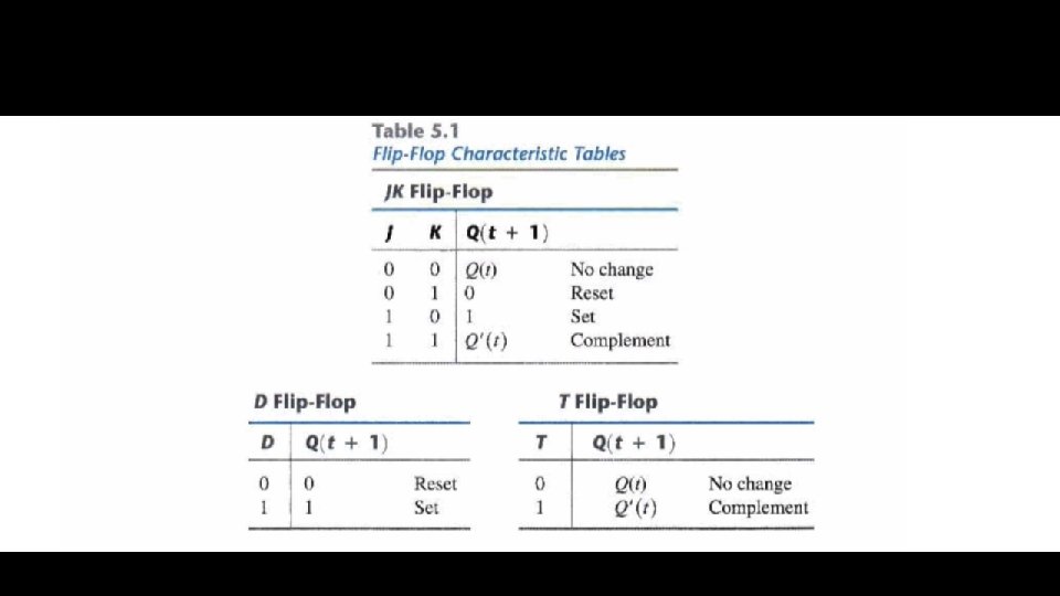
D Flip-flop § D flip-flop: single input D (data) v. D=HIGH a SET state v. D=LOW a RESET state § Q follows D at the clock edge. § Convert S-R flip-flop into a D flip-flop: add an inverter. D CLK S C R Q Q' A positive edge-triggered D flip-flop formed with an S-R flip-flop. D Flip-flop = clock transition LOW to HIGH 24
D Flip-flop § Application: Parallel data transfer. To transfer logic-circuit outputs X, Y, Z to flip-flops Q 1, Q 2 and Q 3 for storage. D CLK X Combinational logic circuit Y D Z CLK D Transfer CLK Q Q 1 = X* Q' Q Q 2 = Y* Q' Q Q 3 = Z* Q' * After occurrence of negative-going transition D Flip-flop 25
J-K Flip-flop § J-K flip-flop: Q and Q' are fed back to the pulsesteering NAND gates. § No invalid state. § Include a toggle state. v. J=HIGH (and K=LOW) a SET state v. K=HIGH (and J=LOW) a RESET state vboth inputs LOW a no change vboth inputs HIGH a toggle J-K Flip-Ffop 26
J-K Flip-flop § J-K flip-flop. J CLK Pulse transition detector K Q Q' § Characteristic table. Q(t+1) = J. Q' + K'. Q J-K Flip-flop 27
T Flip-flop § T flip-flop: single-input version of the J-K flip flop, formed by tying both inputs together. T CLK T Q Pulse transition detector CLK Q' J C K Q Q' § Characteristic table. Q(t+1) = T. Q' + T'. Q T Flip-flop 28
T Flip-flop § Application: Frequency division. High J CLK High J Q CLK C K CLK Q QA QA J C C K K QB QB Divide clock frequency by 2. Divide clock frequency by 4. § Application: Counter T Flip-flop 29
Analysis of Clocked Sequential Circuits : State • State (Keadaan) • State = Nilai output semua flip-flop Contoh AB=00 Keluaran dari dua buah FF 31 / 60
Analysis of Clocked Sequential Circuits : State Equation Contoh: A(t+1) = DA = A(t) x(t)+B(t) x(t) =Ax+Bx B(t+1) = DB = A’(t) x(t) = A’ x y(t) = [A(t)+ B(t)] x’(t) = (A + B) x’ 32 / 60
Analysis of Clocked Sequential Circuits: State Table (Transition Table) Present Input State A 0 0 1 1 B 0 0 1 1 t x 0 1 0 1 Next State A 0 0 0 1 0 1 t+1 B 0 1 0 0 Output y 0 0 1 0 1 0 t A(t+1) = A x + B x B(t+1) = A’ x y(t) = (A + B) x’ 33 / 60
Analysis of Clocked Sequential Circuits : State Table (Transition Table) • Penulisan lain Present State A 0 0 1 1 t B 0 1 Next State Output x=0 x=1 A 0 0 B 0 0 A 0 1 1 1 t+1 B 1 1 0 0 y 0 1 1 1 y 0 0 t A(t+1) = A x + B x B(t+1) = A’ x y(t) = (A + B) x’ 34 / 60
Analysis of Clocked Sequential Circuits : State Table (Transition Table) Present Input State A 0 0 1 1 B 0 0 1 1 t x 0 1 0 1 Next State A 0 0 0 1 0 1 t+1 B 0 1 0 0 Output y 0 0 1 0 1 0 t Present State A 0 0 1 1 t B 0 1 Next State Output x=0 x=1 A 0 0 B 0 0 A 0 1 1 1 t+1 B 1 1 0 0 y 0 1 1 1 y 0 0 t
Analysis of Clocked Sequential Circuits: State Diagram input/output AB 0/0 1/0 0/1 00 10 Present State Next State x=0 Output x=1 x=0 x=1 A B A B y y 0 0 0 1 1 1 0 0 0 1 0 1 1 0 0/1 1/0 0/1 01 1/0 11 1/0 36 / 60
Analysis of Clocked Sequential Circuits « D Flip-Flops Contoh: Present Input State A 0 0 1 1 x 0 0 1 1 y 0 1 0 1 Next State A 0 1 1 0 0 1 x y D CLK Q A(t+1) = DA = A x y 01, 10 00, 11 0 1 00, 11 01, 10 37 / 60
Analysis of Clocked Sequential Circuits « JK Flip-Flops Contoh: Present Next I/P State A B x A B Flip-Flop Inputs JA KA JB KB 0 0 1 0 0 0 1 0 1 1 1 0 0 1 1 0 0 1 1 1 0 0 0 1 1 1 1 1 0 0 0 JA = B JB = x’ KA = B x’ KB = A x A(t+1) = JA Q’A + K’A QA = A’B + AB’ + Ax B(t+1) = JB Q’B + K’B QB = B’x’ + ABx + A’Bx’ 38 / 60
Analysis of Clocked Sequential Circuits « JK Flip-Flops Contoh: Present Next I/P State A B x A B Flip-Flop Inputs JA KA JB KB 0 0 1 0 0 0 1 0 1 1 1 0 0 1 1 0 0 1 1 1 0 0 0 1 1 1 1 1 0 0 0 1 11 00 0 0 01 0 10 1 1 39 / 60
Analysis of Clocked Sequential Circuits « T Flip-Flops Contoh: Present Next F. F I/P O/P State Inputs A B x A B TA TB y 0 0 0 0 0 1 0 1 0 0 1 1 1 0 1 0 0 0 0 1 1 1 0 0 1 1 0 0 1 1 1 TA = B x y =AB TB = x A(t+1) = TA Q’A + T’A QA = AB’ + Ax’ + A’Bx B(t+1) = TB Q’B + T’B QB =x B 40 / 60
Analysis of Clocked Sequential Circuits • T Flip-Flops Present Contoh: State I/P Next F. F O/P State Inputs A B TA TB y A B x 0 0 0 0 0 1 0 0 1 1 0 0 0 1 0 1 1 0 0 1 1 0 1 0 1 1 1 0/0 00 1/0 01 1/1 0/1 1/0 11 10 1/0 0/0 41 / 60
Mealy and Moore Models Mealy Present State A B 0 0 0 1 0 1 1 1 1 I/P x 0 1 0 1 Next O/P State A B y 0 0 1 0 0 0 1 1 0 0 Untuk state yang sama, output berubah bersama input Moore Present State A B 0 0 0 1 0 1 1 1 1 I/P x 0 1 0 1 Next O/P State A B y 0 0 1 0 0 1 1 1 0 0 1 Untuk state yang sama, output tidak berubah bersama input 42 / 60
Moore State Diagram State / Output 0 1 00/0 01/0 1 1 11/1 0 0 10/0 1 0 43 / 60
Timing Diagram 1 0 00/0 A x y 0 B 01/0 1 0 11/1 No effect 0 10/0 1 1 CLK x State A 0 0 1 0 0 0 B 0 1 0 0 1 1 y 44 / 60
Timing Diagram 1/0 00 A x y B 0/0 01 1/0 0/0 11 1/1 0/0 10 1/1 CLK x State A 1 B 0 y 45 / 60
Design of Clocked Sequential Circuits « Contoh: Mendeteksi 3 atau lebih 1 yang muncul berurutan 1 0 S 0 / 0 S 1 / 0 0 0 1 0 S 3 / 1 1 S 2 / 0 State A B S 0 0 0 S 1 0 1 S 2 1 0 S 3 1 1 1 46 / 60
Design of Clocked Sequential Circuits « Contoh: Mendeteksi 3 atau lebih 1 yang muncul berurutan Present Input State A 0 0 1 1 B 0 0 1 1 x 0 1 0 1 Next State A 0 0 0 1 0 1 B 0 1 0 0 0 1 Output y 0 0 0 1 1 1 0 S 0 / 0 S 1 / 0 0 S 3 / 1 1 1 S 2 / 0 1 47 / 60
Design of Clocked Sequential Circuits « Contoh: Mendeteksi 3 atau lebih 1 yang muncul berurutan Present Input State A 0 0 1 1 B 0 0 1 1 x 0 1 0 1 Next State A 0 0 0 1 0 1 B 0 1 0 0 0 1 Output y 0 0 0 1 1 Synthesis using D Flip-Flops A(t+1) = DA (A, B, x) = ∑ (3, 5, 7) B(t+1) = DB (A, B, x) = ∑ (1, 5, 7) y (A, B, x) = ∑ (6, 7) 48 / 60
Design of Clocked Sequential Circuits with D F. F. « Contoh: Mendeteksi 3 atau lebih 1 yang muncul berurutan Synthesis using D Flip-Flops DA (A, B, x) = ∑ (3, 5, 7) =Ax+Bx DB (A, B, x) = ∑ (1, 5, 7) B 0 0 1 0 A 0 1 1 0 x 0 1 0 0 = A x + B’ x y (A, B, x) = ∑ (6, 7) =AB B B A 0 1 1 0 x 0 0 A 0 0 1 1 x 49 / 60
Design of Clocked Sequential Circuits with D F. F. « Contoh: Mendeteksi 3 atau lebih 1 yang muncul berurutan Synthesis using D Flip-Flops DA = A x + B x DB = A x + B’ x y =AB 50 / 60
Flip-Flop Excitation Tables Present Next State Q(t) Q(t+1) 0 0 0 1 1 F. F. Input D 0 1 Present Next State F. F. Input Q(t) Q(t+1) J K 0 x 0 0 1 x 0 1 1 0 x 1 1 1 x 0 Q(t) Q(t+1) 0 0 0 1 1 0 0 (No change) 0 1 (Reset) 1 0 (Set) 1 1 (Toggle) 0 1 (Reset) 1 1 (Toggle) 0 0 (No change) 1 0 (Set) T 0 1 1 0 51 / 60
Design of Clocked Sequential Circuits with JK F. F. « Contoh: Mendeteksi 3 atau lebih 1 yang muncul berurutan Present Input State A 0 0 1 1 B 0 0 1 1 x 0 1 0 1 Next State A 0 0 0 1 0 1 B JA 0 0 1 0 x 1 x Flip-Flop Inputs KA x x 1 0 JB KB 0 x 1 x 1 0 x 1 x 0 Synthesis using JK F. F. JA (A, B, x) = ∑ (3) d. JA (A, B, x) = ∑ (4, 5, 6, 7) KA (A, B, x) = ∑ (4, 6) d. KA (A, B, x) = ∑ (0, 1, 2, 3) JB (A, B, x) = ∑ (1, 5) d. JB (A, B, x) = ∑ (2, 3, 6, 7) KB (A, B, x) = ∑ (2, 3, 6) d. KB (A, B, x) = ∑ (0, 1, 4, 5) 52 / 60
Design of Clocked Sequential Circuits with JK F. F. « Contoh: Mendeteksi 3 atau lebih 1 yang muncul berurutan Synthesis using JK Flip-Flops JA = B x KA = x’ JB = x KB = A’ + x’ B B 0 0 1 0 x x A x x x B 0 1 x x A 1 0 0 1 x B x x 1 1 A 0 1 x x x A x x 0 1 x 53 / 60
Design of Clocked Sequential Circuits with T F. F. « Contoh: Mendeteksi 3 atau lebih 1 yang muncul berurutan Present Input State A 0 0 1 1 B 0 0 1 1 x 0 1 0 1 Next State A 0 0 0 1 0 1 B 0 1 0 0 0 1 F. F. Input TA 0 0 0 1 1 0 TB 0 1 1 1 0 Synthesis using T Flip-Flops TA (A, B, x) = ∑ (3, 4, 6) TB (A, B, x) = ∑ (1, 2, 3, 5, 6) 54 / 60
Design of Clocked Sequential Circuits with T F. F. « Contoh: Mendeteksi 3 atau lebih 1 yang muncul berurutan Synthesis using T Flip-Flops TA = A x’ + A’ B x TB = A’ B + B x B B 0 0 1 1 1 A 1 0 0 1 x A 0 1 x 55 / 60
Homework • Mano • Chapter 5 • • • 5 -1 5 -3 5 -6 5 -8 5 -9 56 / 60
Homework 5 -3 Tunjukkan bahwa output komplemen JK flip-flop adalah sebagai berikut: Q’(t+1) = J’Q + K Q 5 -6 Sebuah rangkaian sekuensial dibuat dengan menggunakan dua buah DFF, A dan B; dua buah input x dan y; dan satu output z. Persamaan state dan persamaan outputnya adalah sebagai berikut: A(t+1) = x’ y + x A B(t+1) = x’ B + x A z=B (a) Gambarlah diagram logic-nya! (b) Buatlah state table –nya!. (c) Gambarkan state diagramnya 57 / 60
Homework 5 -8 Buatlah state table dan state diagram untuk ragkaian logika berikut ini dan jelaskan kegunaan rangkaiannya. 58 / 60
Homework 5 -9 Sebuah rangkaian sekuensial mempunyai dua buah JK flip-flop A dan B serta sebuah input x. Rangkaian tersebut mempunyai persamaan input : JA = x KA = B’ JB = x KB = A (a) Bagimanakan persamaan state untuk A(t+1) dan B(t+1) dengan melakuakan substitusi persamaan input untuk variable J dan K (b) Gambarkan State Diagramnya 59 / 60